| Secciones |
|---|
| Foros Electrónica |
|
|
| Boletines de correo |
 |
© Semiconductor Components Industries, LLC, 2011
September, 2011 - Rev. 10
1
Publication Order Number:
2N5060/D
2N5060 Series
Sensitive Gate
Silicon Controlled Rectifiers
Reverse Blocking Thyristors
Annular PNPN devices designed for high volume consumer
applications such as relay and lamp drivers, small motor controls, gate
drivers for larger thyristors, and sensing and detection circuits.
Supplied in an inexpensive plastic TO-92/TO-226AA package which
is readily adaptable for use in automatic insertion equipment.
Features
Sensitive Gate Trigger Current - 200
mA Maximum
Low Reverse and Forward Blocking Current - 50
mA Maximum,
T
C
= 110
°C
Low Holding Current - 5 mA Maximum
Passivated Surface for Reliability and Uniformity
These are Pb-Free Devices
MAXIMUM RATINGS
(T
J
= 25 °C unless otherwise noted)
Rating
Symbol
Value
Unit
Peak Repetitive Off-State Vo
(T
J
= *40 to 110 °C, Sine Wave,
50 to 60 Hz, R
GK
= 1 kW)
2N5060
2N5061
2N5062
2N5064
V
DRM,
V
RRM
30
60
100
200
V
On-State Current RMS (180 ° Conduction
Angles; T
C
= 80 °C)
I
T(RMS)
0.8
A
*Average On-State Current
(180 ° Conduction Angles)
(T
C
= 67 °C)
(T
C
= 102 °C)
I
T(AV)
0.51
0.255
A
*Peak Non-repetitive Surge Current,
T
A
= 25 °C (1/2 cycle, Sine Wave, 60 Hz)
I
TSM
10
A
Circuit Fusing Considerations (t = 8.3 ms)
I
2
t
0.4
A
2
s
*Average On-State Current
(180 ° Conduction Angles)
(T
C
= 67 °C)
(T
C
= 102 °C)
I
T(AV)
0.51
0.255
A
*Forward Peak Gate Power (Pulse Width v
1.0 msec; T
A
= 25 °C)
P
GM
0.1
W
*Forward Average Gate Power
(T
A
= 25 °C, t = 8.3 ms)
P
G(AV)
0.01
W
*Forward Peak Gate Current (Pulse Width
v 1.0 msec; T
A
= 25 °C)
I
GM
1.0
A
*Reverse Peak Gate Voltage (Pulse Width
v 1.0 msec; T
A
= 25 °C)
V
RGM
5.0
V
*Operating Junction Temperature Range
T
J
-40 to
+110
°C
*Storage Temperature Range
T
stg
-40 to
+150
°C
Stresses exceeding Maximum Ratings may damage the device. Maximum
Ratings are stress ratings only. Functional operation above the Recommended
Operating Conditions is not implied. Extended exposure to stresses above the
Recommended Operating Conditions may affect device reliability.
1. V
DRM
and V
RRM
for all types can be applied on a continuous basis. Ratings
apply for zero or negative gate voltage; however, positive gate voltage shall
not be applied concurrent with negative potential on the anode. Blocking
voltages shall not be tested with a constant current source such that the
voltage ratings of the devices are exceeded.
*Indicates JEDEC Registered Data.
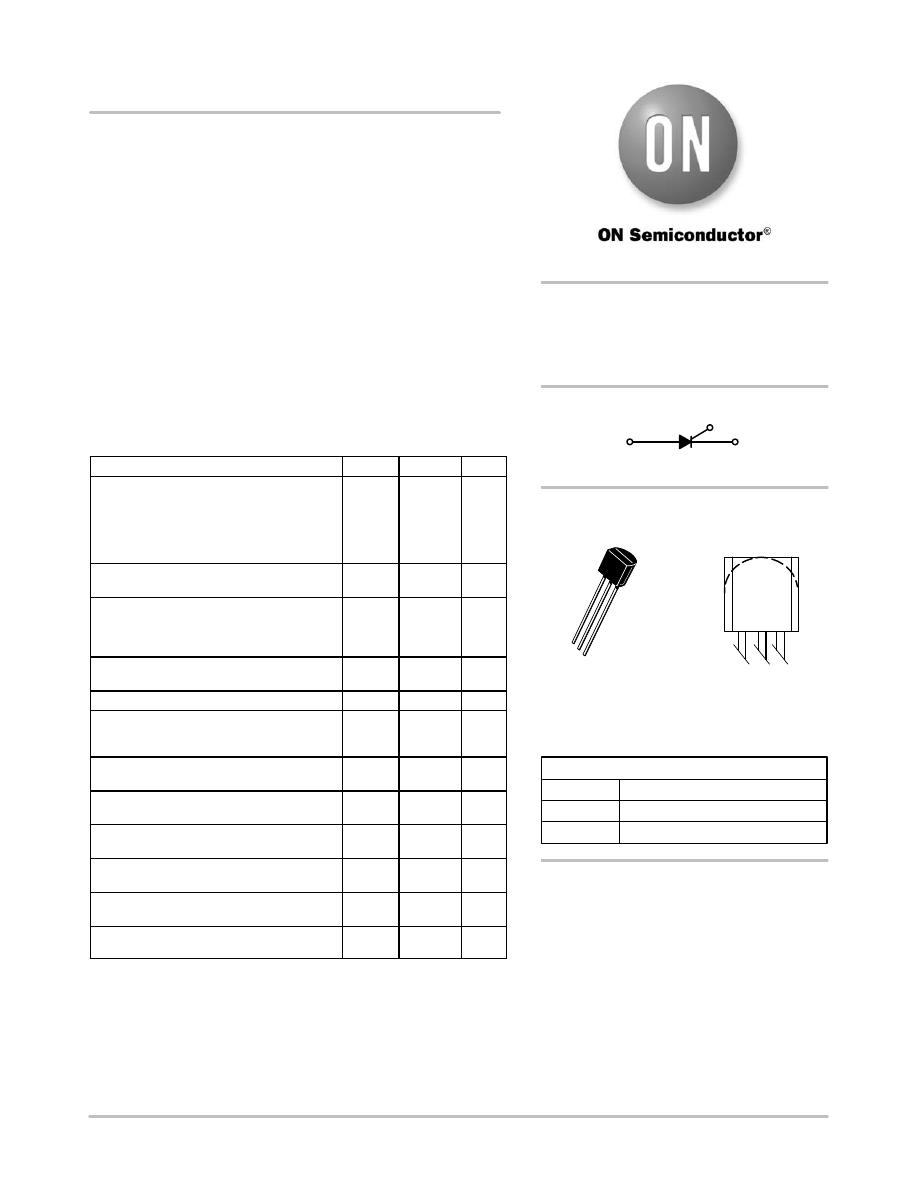
SILICON CONTROLLED
RECTIFIERS
0.8 A RMS, 30 - 200 V
K
G
A
See detailed ordering and shipping information in the package
dimensions section
ORDERING INFORMATION
TO-92
CASE 29
STYLE 10
50xx
Specific Device Code
Y
= Year
WW
= Work Week
MARKING
DIAGRAM
2N
50xx
YWW
PIN ASSIGNMENT
1
2
3
Gate
Anode
Cathode
http://onsemi.com
1 2
3
2N5060 Series
http://onsemi.com
2
THERMAL CHARACTERISTICS
Characteristic
Symbol
Max
Unit
*Thermal Resistance, Junction-to-
R
qJC
75
°C/W
Thermal Resistance, Junction-to-Ambient
R
qJA
200
°C/W
2. This measurement is made with the case mounted flat side down on a heatsink and held in position by means of a metal clamp over the
curved surface.
*Indicates JEDEC Registered Data.
ELECTRICAL CHARACTERISTICS
(T
C
= 25 °C unless otherwise noted)
Characteristic
Symbol
Min
Typ
Max
Unit
OFF CHARACTERISTICS
*Peak Repetitive Forward or Reverse Blocking Current
(V
AK
= Rated V
DRM
or V
RRM
)
T
C
= 25 °C
T
C
= 110 °C
I
DRM
, I
RRM
-
-
-
-
10
50
mA
mA
ON CHARACTERISTICS
*Peak Forward On-State V
(I
TM
= 1.2 A peak @ T
A
= 25 °C)
V
TM
-
-
1.7
V
Gate Trigger Current
*(V
AK
= 7.0 Vdc, R
L
= 100 W)
T
C
= 25 °C
T
C
= -40 °C
I
GT
-
-
-
-
200
350
mA
Gate Trigger V
T
C
= 25 °C
*(V
AK
= 7.0 Vdc, R
L
= 100 W)
T
C
= -40 °C
V
GT
-
-
-
-
0.8
1.2
V
*Gate Non-Trigger Voltage
(V
AK
= Rated V
DRM
, R
L
= 100 W) T
C
= 110 °C
V
GD
0.1
-
-
V
Holding Current
T
C
= 25 °C
*(V
AK
= 7.0 Vdc, initiating current = 20 mA)
T
C
= -40 °C
I
H
-
-
-
-
5.0
10
mA
Turn-On Time
Delay Time
Rise Time
(I
GT
= 1.0 mA, V
D
= Rated V
DRM
,
Forward Current = 1.0 A, di/dt = 6.0 A/ms
t
d
t
r
-
-
3.0
0.2
-
-
ms
Turn-Off Time
(Forward Current = 1.0 A pulse,
Pulse Width = 50 ms,
0.1% Duty Cycle, di/dt = 6.0 A/ms,
dv/dt = 20 V/ms, I
GT
= 1 mA)
2N5060, 2N5061
2N5062, 2N5064
t
q
-
-
10
30
-
-
ms
DYNAMIC CHARACTERISTICS
Critical Rate of Rise of Off-State Voltage
(Rated V
DRM
, Exponential, R
GK
= 1 kW)
dv/dt
-
30
-
V/ms
*Indicates JEDEC Registered Data.
3. R
GK
= 1000 W is included in measurement.
4. Forward current applied for 1 ms maximum duration, duty cycle p 1%.
5. R
GK
current is not included in measurement.
2N5060 Series
http://onsemi.com
3
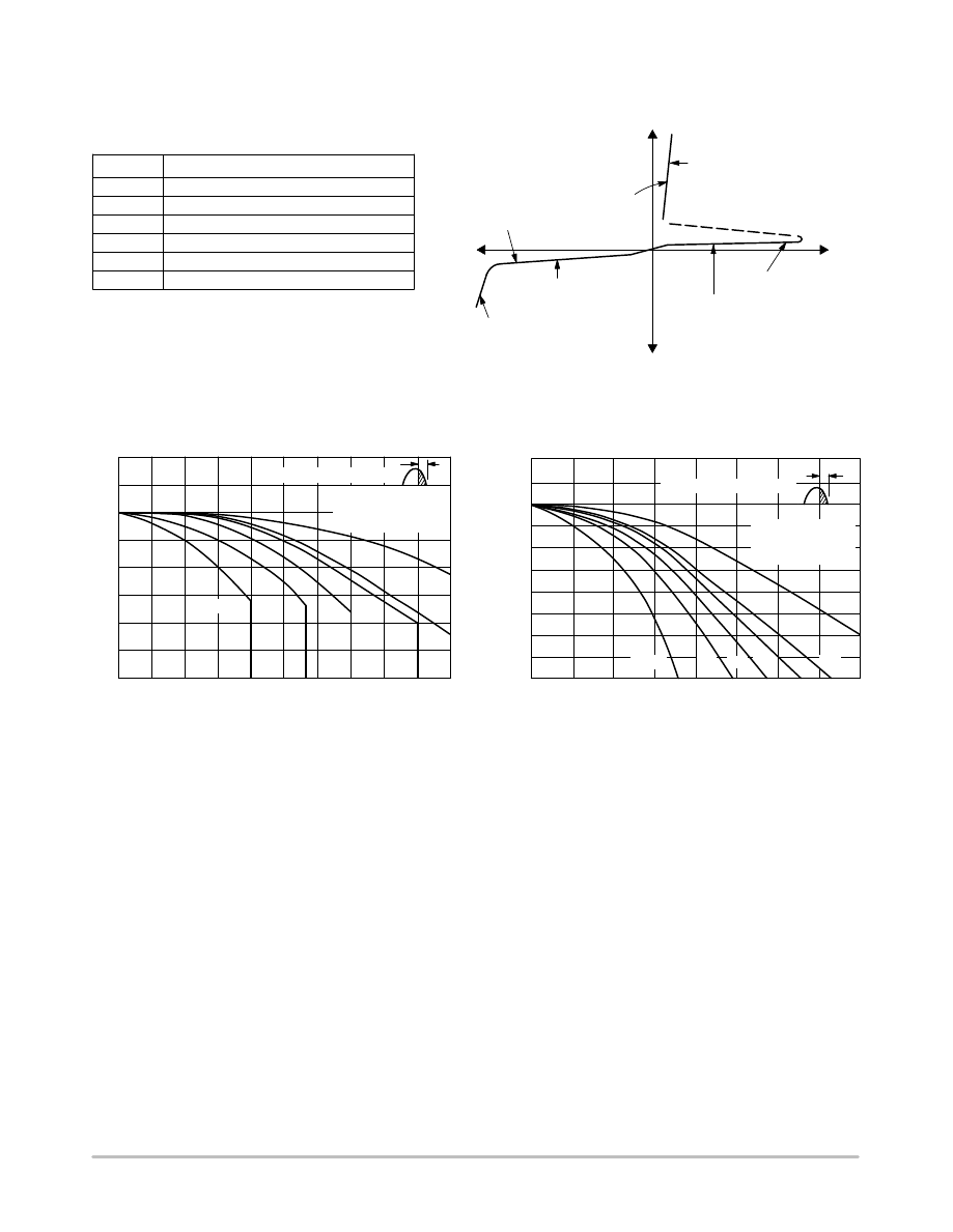
+ Current
+ Voltage
V
TM
I
DRM
at V
DRM
I
H
Symbol
Parameter
V
DRM
Peak Repetitive Off State Forward Voltage
I
DRM
Peak Forward Blocking Current
V
RRM
Peak Repetitive Off State Reverse Voltage
I
RRM
Peak Reverse Blocking Current
V
TM
Peak on State Voltage
I
H
Holding Current
Voltage Current Characteristic of SCR
Anode +
on state
Reverse Blocking Region
(off state)
Reverse Avalanche Region
Anode -
Forward Blocking Region
I
RRM
at V
RRM
(off state)
120
50
60
70
80
90
100
110
0
0.1
0.2
0.3
0.4
130
0.5
I
T(AV)
, AVERAGE ONSTATE CURRENT (AMP)
a
dc
110
30
50
70
90
130
dc
a
0
0.1
0.2
0.3
0.4
I
T(AV)
, AVERAGE ONSTATE CURRENT (AMP)
T C
, MAXIMUM
ALLOW
ABLE CASE
TEMPERA
TURE ( C)
°
T A
, MAXIMUM ALLOW
ABLE AMBIENT
°
TEMPERA
TURE ( C)
a = 30 °
a = 30 °
60
° 90 °
90
°
120
°
120
°
180
°
CASE MEASUREMENT
POINT - CENTER OF
FLAT PORTION
60
°
180
°
TYPICAL PRINTED
CIRCUIT BOARD
MOUNTING
a = CONDUCTION ANGLE
a = CONDUCTION ANGLE
Figure 1. Maximum Case Temperature
Figure 2. Maximum Ambient Temperature
CURRENT DERATING
2N5060 Series
http://onsemi.com
4
P
(A
V)
, MAXIMUM
A
VERAGE POWER
DISSIP
A
TION (W
A
TTS)
5.0
0.05
0.01
0.02
0
0.5
1.0
1.5
2.0
3.0
2.5
v
T
, INSTANTANEOUS ONSTATE VOLTAGE (VOLTS)
0.07
0.03
0.1
0.2
0.3
0.5
0.7
1.0
2.0
5.0
25
°C
T
J
= 110
°C
30
7.0
1.0
3.0
2.0
10
1.0
2.0
3.0
5.0 7.0
10
20
50 70
100
0
0.2
0.4
0.6
a
0.1
0.4
dc
0.8
0
0.2
0.5
a = CONDUCTION ANGLE
0.3
NUMBER OF CYCLES
I
T(AV)
, AVERAGE ONSTATE CURRENT (AMP)
i T
, INST
ANT
ANEOUS ONST
A
TE CURRENT
(AMP)
I TSM
, PEAK SURGE CURRENT
(AMP)
a = 30 °
60
°
90
°
120
°
180
°
Figure 3. Typical Forward Voltage
Figure 4. Maximum Non-Repetitive Surge Current
Figure 5. Power Dissipation
CURRENT DERATING
2N5060 Series
http://onsemi.com
5
0.7
0.3
0.4
0.5
0.6
0.8
V
AK
= 7.0 V
R
L
= 100
R
GK
= 1.0 k
3.0
0.8
0.4
0.6
1.0
2.0
50
0
-75
-50
-25
4.0
25
100
75
110
T
J
, JUNCTION TEMPERATURE (
°C)
2N5060,61
100
V
AK
= 7.0 V
R
L
= 100
R
GK
= 1.0 k
0.2
0.5
1.0
2.0
5.0
10
20
50
200
V
AK
= 7.0 V
R
L
= 100
2N506264
2N506061
TYPICAL CHARACTERISTICS
50
0
-75
-50
-25
25
100
75
110
T
J
, JUNCTION TEMPERATURE (
°C)
50
0
-75
-50
-25
25
100
75
T
J
, JUNCTION TEMPERATURE (
°C)
V
G
, GA
TE
TRIGGER VOL
TAGE (VOL
TS)
I GT
, GA
TE
TRIGGER CURRENT
(NORMALIZED)
I H
, HOLDING CURRENT
(NORMALIZED)
2N506264
0.02
0.2
20
10
5.0
2.0
1.0
0.05
0.01
0.002
0.005
0.5
0.02
0.01
0.5
0.1
0.05
0.1
0.2
t, TIME (SECONDS)
1.0
r(t), TRANSIENT
THERMAL
RESIST
ANCE
NORMALIZED
110
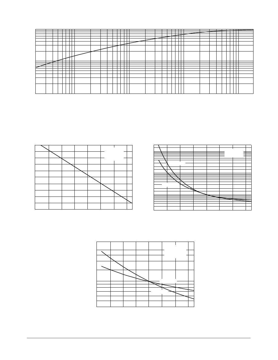
Figure 6. Thermal Response
Figure 7. Typical Gate Trigger Voltage
Figure 8. Typical Gate Trigger Current
Figure 9. Typical Holding Current

2N5060 Series
http://onsemi.com
6
ORDERING INFORMATION
Device
Package
Shipping
2N5060G
TO-92
(Pb-Free)
5000 Units / Box
2N5060RLRA
TO-92
2000 / Tape & Reel
2N5060RLRAG
TO-92
(Pb-Free)
2000 / Tape & Reel
2N5060RLRMG
TO-92
(Pb-Free)
2000 / Ammo Pack
2N5061G
TO-92
(Pb-Free)
5000 Units / Box
2N5061RLRAG
TO-92
(Pb-Free)
2000 / Tape & Reel
2N5062G
TO-92
(Pb-Free)
5000 Units / Box
2N5062RLRAG
TO-92
(Pb-Free)
2000 / Tape & Reel
2N5064RLRMG
TO-92
(Pb-Free)
2000 / Ammo Pack
2N5064RLRAG
TO-92
(Pb-Free)
2000 / Tape & Reel
2N5064G
TO-92
(Pb-Free)
5000 Units / Box
For information on tape and reel specifications, including part orientation and tape sizes, please refer to our Tape and Reel Packaging
Specifications Brochure, BRD8011/D.

2N5060 Series
http://onsemi.com
7
PACKAGE DIMENSIONS
TO-92 (TO-226)
CASE 29-11
ISSUE AM
NOTES:
1. DIMENSIONING AND TOLERANCING PER ANSI
Y14.5M, 1982.
2. CONTROLLING DIMENSION: INCH.
3. CONTOUR OF PACKAGE BEYOND DIMENSION R
IS UNCONTROLLED.
4. LEAD DIMENSION IS UNCONTROLLED IN P AND
BEYOND DIMENSION K MINIMUM.
R
A
P
J
L
B
K
G
H
SECTION X-X
C
V
D
N
N
X X
SEATING
PLANE
DIM
MIN
MAX
MIN
MAX
MILLIMETERS
INCHES
A
0.175
0.205
4.45
5.20
B
0.170
0.210
4.32
5.33
C
0.125
0.165
3.18
4.19
D
0.016
0.021
0.407
0.533
G
0.045
0.055
1.15
1.39
H
0.095
0.105
2.42
2.66
J
0.015
0.020
0.39
0.50
K
0.500
---
12.70
---
L
0.250
---
6.35
---
N
0.080
0.105
2.04
2.66
P
---
0.100
---
2.54
R
0.115
---
2.93
---
V
0.135
---
3.43
---
1
NOTES:
1. DIMENSIONING AND TOLERANCING PER
ASME Y14.5M, 1994.
2. CONTROLLING DIMENSION: MILLIMETERS.
3. CONTOUR OF PACKAGE BEYOND
DIMENSION R IS UNCONTROLLED.
4. LEAD DIMENSION IS UNCONTROLLED IN P
AND BEYOND DIMENSION K MINIMUM.
R
A
P
J
B
K
G
SECTION X-X
C
V
D
N
X X
SEATING
PLANE
DIM
MIN
MAX
MILLIMETERS
A
4.45
5.20
B
4.32
5.33
C
3.18
4.19
D
0.40
0.54
G
2.40
2.80
J
0.39
0.50
K
12.70
---
N
2.04
2.66
P
1.50
4.00
R
2.93
---
V
3.43
---
1
T
STRAIGHT LEAD
BULK PACK
BENT LEAD
TAPE & REEL
AMMO PACK
STYLE 10:
PIN 1. CATHODE
2. GATE
3. ANODE
ON Semiconductor and are registered trademarks of Semiconductor Components Industries, LLC (SCILLC). SCILLC reserves the right to make changes without further notice
to any products herein. SCILLC makes no warranty, representation or guarantee regarding the suitability of its products for any particular purpose, nor does SCILLC assume any liability
arising out of the application or use of any product or circuit, and specifically disclaims any and all liability, including without limitation special, consequential or incidental damages.
Typical parameters which may be provided in SCILLC data sheets and/or specifications can and do vary in different applications and actual performance may vary over time. All
operating parameters, including Typicals must be validated for each customer application by customers technical experts. SCILLC does not convey any license under its patent rights
nor the rights of others. SCILLC products are not designed, intended, or authorized for use as components in systems intended for surgical implant into the body, or other applications
intended to support or sustain life, or for any other application in which the failure of the SCILLC product could create a situation where personal injury or death may occur. Should
Buyer purchase or use SCILLC products for any such unintended or unauthorized application, Buyer shall indemnify and hold SCILLC and its officers, employees, subsidiaries, affiliates,
and distributors harmless against all claims, costs, damages, and expenses, and reasonable attorney fees arising out of, directly or indirectly, any claim of personal injury or death
associated with such unintended or unauthorized use, even if such claim alleges that SCILLC was negligent regarding the design or manufacture of the part. SCILLC is an Equal
Opportunity/Affirmative Action Employer. This literature is subject to all applicable copyright laws and is not for resale in any manner.
PUBLICATION ORDERING INFORMATION
N. American Technical Support: 800-282-9855 Toll Free
USA/Canada
Europe, Middle East and Africa Technical Support:
Phone: 421 33 790 2910
Japan Customer Focus Center
Phone: 81-3-5773-3850
2N5060/D
LITERATURE FULFILLMENT:
Literature Distribution Center for ON Semiconductor
P.O. Box 5163, Denver, Colorado 80217 USA
Phone: 303-675-2175 or 800-344-3860 Toll Free USA/Canada
Fax: 303-675-2176 or 800-344-3867 Toll Free USA/Canada
Email: orderlit@onsemi.com
ON Semiconductor Website: www.onsemi.com
Order Literature: http://www.onsemi.com/orderlit
For additional information, please contact your local
Sales Representative

