Geneva – STMicroelectronics today
revealed successful fabrication of the first of a family of configurable System-on-Chip ICs that addresses a variety
of applications, including digital engines for printers, scanners and other embedded control applications, and
provides ST customers with a complete roadmap to cover current and future needs.
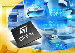
Based upon ST’s Structured Processor Enhanced Architecture (SPEAr), the device integrates an ARM core with
a full set of IP (intellectual property) blocks and a configurable logic block that allows very fast customization
of critical functions in a fraction of the time and at a fraction of the cost required by a full custom design
approach, but with a comparable level of flexibility and performance.
The family
is based on industry-standard ARM cores that maximize the reuse of existing hardware and software blocks. The
architecture includes a number of proven IPs for connectivity, memory interfaces, and a high-performance internal
bus system. Finally a customizable embedded-logic block allows quick development of optimized solutions for specific
markets by allowing customers to add their own proprietary IP to an ASSP (application-specific standard product)
without embarking on a full ASIC design.
“SPEAr is a new concept in the
market. This innovative family allows easy access to state-of-the-art technology together with high performance and
full customization, closing the gap between the high flexibility of the full ASIC approach with the low cost of
ownership of the ASSP approach,” said Vittorio Peduto, General Manager of ST’s Computer Systems
Division. “It reduces design cycle times to a few weeks and turnaround times that can be as short as few days,
using e-beam prototyping, with a very low NRE. Full mass production can ramp up in six to eight weeks time from the
final RTL availability. The SPEAr technology allows unprecedented time to market, which has been impossible so far
for this level of complexity and performance.”
|  | |
The new device includes: an ARM946ES running at 192MHz with 8-kbyte of data
cache, instruction cache, data-TCM (Tightly Coupled Memory) and instruction-TCM, respectively; three USB2.0 ports
(including both host and device ports); an Ethernet 10/100 MAC; a 16-channel 8-bit A/D converter; an I2C interface;
three UARTs; memory interfaces; and 400-kgate equivalent programmable logic.
Samples of this first
member of the family are already available, with pricing in the range of $13 in volume quantities. Full evaluation
boards will be shipping in September. A special dual-mode development environment has been implemented to allow ST
customers to develop their solution with an external FPGA, and then verify the solution and map it into the
configurable logic inside the chip, both quickly and easily. Additionally, to provide more flexibility in the
development ST will also provide a simplified version with the programmable logic completely removed for any device
in the family.
|
