| Secciones |
|---|
|
|
| Foros Electrónica |
| Alguien dijo ... |
| La ciencia es como la tierra; solo se puede poseer un poco de ella. François Marie Arouet(Voltaire - 1694-1778). Escritor y filósofo francés. |
| Contacto |
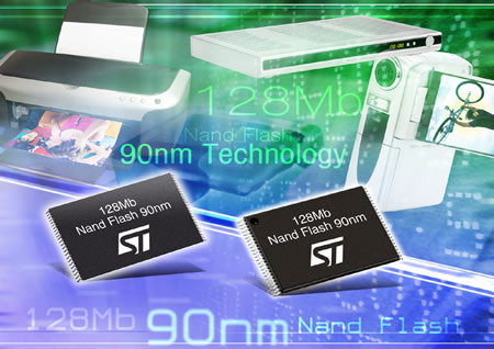
| STMicroelectronics Moves 128-Mbit NAND Flash Chip to 90nm Production Technology | ||||||||
Geneva – STMicroelectronics announced that production of its 128-Mbit NAND Flash device – the NAND128W3A2BN6E – has been transferred to 90nm process technology. The shrink to 90nm reduces both the cost and the power consumption of the memory chip, which is widely used in cost-sensitive consumer equipment such as Digital Still Cameras, Audio Recorders, PDAs, Set-Top Boxes (STBs), Printers, and bundled Flash Cards. The NAND128 is currently the only 128-Mbit Flash memory on the market to be produced in 90nm technology. The new chip confirms ST’s commitment to continuing product development of its low density ‘Small-Page’ NAND Flash memory products, in support of customers already using the family in volume production. The NAND128W3A2BN6E is a 3V product, in a TSOP package, intended for consumer applications. Other family members – the 256-Mbit, 512-Mbit, both in 3V and in 1.8V versions – will also be moved from 120nm to 90nm technology in the coming months. The NAND128 provides ultra-fast
data throughput and erase capability.
The Address lines and Data Input/Output signals of all members of the
family are multiplexed onto an 8-bit bus, reducing pin count and allowing
the use of a modular NAND
interface, which enables manufacturers to
produce variations of systems that use higher (or lower) density
devices
without changing the footprint.
The device has the ‘Chip Enable Don’t Care’ feature, which simplifies the microcontroller interface and streamlines the use of NAND Flash in combination with other types of memory such as NOR Flash and SRAM. A unique device ID can be factory programmed, and a User Programmable Serial number supports increased security in the target application. The NAND128W3A2BN6E is available in volume now with pricing in the range of $4 to $4.5 in a lead-free TSOP48 package, and is characterized for the -40 to +85 degrees C temperature range.
| ||||||||
Martes, 30 Agosto, 2005 - 01:01 | ||||||||
 | ||||||||