| Secciones |
|---|
| Foros Electrónica |
|
|
| Boletines de correo |
 |

T4-LDS-0075, Rev. 3 (5/24/13)
�2013 Microsemi Corporation
Page 1 of 8
1N2970B - 1N3015B and
1N3993A - 1N3998A
Available on
commercial
versions
10 Watt Zener Diodes
Qualified per MIL-PRF-19500/124
Qualified Levels:
JAN, JANTX, and
JANTXV
DESCRIPTION
The JEDEC registered 1N2970B through 1N3015B and 1N3993A through 1N3998A series are
10W Zener diodes with voltage regulation values between 3.9 and 200V. They are available
in JAN, JANTX, and JANTXV military qualification grades on most voltage values.
DO-213AA
(DO-4)
Package
Important: For the latest information, visit our websit
FEATURES
�
Internal solder bond construction.
�
Hermetically sealed (welded).
�
Zener regulation voltages from 3.9 V to 200 V.
�
Standard and reverse polarities are available.
�
Consult factory for surface mount equivalents.
�
JAN, JANTX, and JANTXV qualifications are available per MIL-PRF-19500/124.
�
RoHS compliant devices available by adding ��e3�� suffix (commercial grade only).
APPLICATIONS / BENEFITS
�
Regulates voltage over a broad range of current and temperature.
�
Standard voltage tolerances are +/- 5%.
�
Nonsensitive to ESD per MIL-STD-750 method 1020.
�
Inherently radiation hard as described in Microsemi
MAXIMUM RATINGS
MSC - Lawrence
6 Lake Street,
Lawrence, MA 01841
Tel: 1-800-446-1158
(978) 620-2600
Fax: (978) 689-0803
MSC - Ireland
Gort Road Business Park,
Ennis, Co. Clare, Ireland
Tel: +353 (0) 65 6840044
Fax: +353 (0) 65 6822298
Website:
Parameters/Test Conditions
Symbol
Value
Unit
Junction Temperature
T
J
-65 to +175
o
C
Storage Temperature
T
STG
-65 to +200
o
C
Thermal Resistance Junction-to-Case
R
ӨJC
12
o
C/W
Steady-State Power Dissipation @ T
C
= +55 �C
(1)
P
D
10
W
Forward Voltage @ 2.0 A
V
F
1.5
V
Solder Pad Temperature @ 10 s
T
SP
260
�C
NOTES: 1. Derate at 0.083 W/ �C above +55 �C.
T4-LDS-0075, Rev. 3 (5/24/13)
�2013 Microsemi Corporation
Page 2 of 8
1N2970B - 1N3015B and
1N3993A - 1N3998A
MECHANICAL and PACKAGING
� CASE: Industry standard DO-4, (DO-203AA), 7/16�� hex, stud with 10-32 threads, welded, hermetically sealed metal and glass.
� TERMINALS: Tin-lead plated or RoHS compliant matte-tin plating (commercial grade only) on nickel.
� POLARITY: 1N2970B - 1N3015B: Std. Polarity is anode to stud. Reverse polarity (cathode to stud) indicated by suffix ��RB��.
1N3993A - 1N3998A: Std. Polarity is cathode to stud. Reverse polarity (anode to stud) indicated by suffix ��RA��.
� MOUNTING HARDWARE: Consult factory for optional insulator, bushing solder terminal, washers, and nut.
� WEIGHT: Approximately 7.5 grams.
� S
on last page.
PART NOMENCLATURE
1N2970 - 1N3015 series only:
JAN 1N2970 R B e3
Reliability Level
JAN = JAN level
JANTX = JANTX level
JANTXV = JANTXV level
Blank = Commercial
JEDEC type number
(s
e)
RoHS Compliance
e3 = RoHS compliant (available
on commercial grade only)
Blank = non-RoHS compliant
5% Tolerance
(Consult factory for other
tolerances)
Polarity
blank = Standard (Anode to
Stud)
R = Reverse (Cathode to Stud)
1N3993 - 1N3998 series only:
JAN 1N3993 R A e3
Reliability Level
JAN = JAN level
JANTX = JANTX level
JANTXV = JANTXV level
Blank = Commercial
JEDEC type number
(s
e)
RoHS Compliance
e3 = RoHS compliant (available
on commercial grade only)
Blank = non-RoHS compliant
5% Tolerance
(Consult factory for other
tolerances)
Polarity
blank = Standard (Cathode to
Stud)
R = Reverse (Anode to Stud)
T4-LDS-0075, Rev. 3 (5/24/13)
�2013 Microsemi Corporation
Page 3 of 8
1N2970B - 1N3015B and
1N3993A - 1N3998A
SYMBOLS & DEFINITIONS
Symbol
Definition
I
ZT
Regulator Current: The dc regulator current (I
Z
), at a specified test point (I
ZT
), near breakdown knee (I
ZK
).
I
R
Reverse Current: The maximum reverse (leakage) current that will flow at the specified voltage and temperature.
I
ZM
Maximum Regulator (Zener) Current: The maximum rated dc current for the specified power rating.
V
F
Maximum Forward Voltage: The maximum forward voltage the device will exhibit at a specified current.
V
R
Reverse Voltage: The reverse voltage dc value, no alternating component.
V
Z
Zener Voltage: The Zener voltage the device will exhibit at a specified current (I
Z
) in its breakdown region.
Z
ZT
or Z
ZK
Dynamic Impedance: The small signal impedance of the diode when biased to operate in its breakdown region at a
specified rms current modulation (typically 10% of I
ZT
or I
ZK
) and superimposed on I
ZT
or I
ZK
respectively.
T4-LDS-0075, Rev. 3 (5/24/13)
�2013 Microsemi Corporation
Page 4 of 8
1N2970B - 1N3015B and
1N3993A - 1N3998A
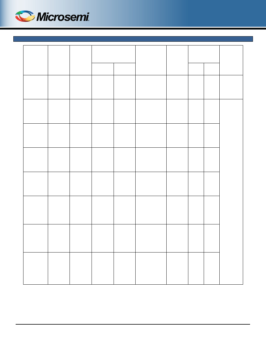
ELECTRICAL CHARACTERISTICS
JEDEC
TYPE NO.
(Note 1)
NOMINAL
ZENER
VOLTAGE
V
Z
@
I
ZT
(Note 2)
Volts
ZENER
TEST
CURRENT
(
I
ZT
)
mA
MAX. DYNAMIC
IMPEDANCE
(Note 3)
MAX DC ZENER
CURRENT
(
I
ZM
) @ 25
o
C
Stud Temp.
(Note 4)
mA
TEMP.
COEFF.
α
VZ
%/
o
C
MAX**
REVERSE
CURRENT
I
R
@
V
R
POLARITY
Z
ZT
@ I
ZT
Ohms
Z
ZK
@
1mA (I
ZK
)
Ohms
�A
Volts
��1N3993A
��1N3994A
��1N3995A
��1N3996A
��1N3997A
��1N3998A
3.9
4.3
4.7
5.1
5.6
6.2
640
580
530
490
445
405
2.0
1.5
1.2
1.1
1.0
1.1
400
400
550
550
600
700
2440
2200
2000
1840
1680
1520
-0.060
-0.050
+0.025
+0.030
+0.040
+0.045
100
100
50
10
10
10
0.5
0.5
1.0
1.0
1.0
2.0
STD.
POLARITY
CATHODE
TO
STUD
��1N2970B
��1N2971B
��1N2972B
��1N2973B
��1N2974B
��1N2975B
6.8
7.5
8.2
9.1
10
11
370
335
305
275
250
230
1.2
1.3
1.5
2.0
3
3
500
250
250
250
250
250
1500
1350
1180
1100
980
890
+0.057
+0.067
+0.070
+0.075
+0.081
+0.085
150
100
50
25
25
10
5.2
5.7
6.2
6.9
7.6
8.4
STD.
POLARITY
ANODE
TO STUD
��1N2976B
��1N2977B
1N2978B
��1N2979B
��1N2980B
1N2981B
12
13
14
15
16
17
210
190
180
170
155
145
3
3
3
3
4
4
250
250
250
250
250
250
820
750
600
640
605
500
+0.079
+0.080
+0.070
+0.082
+0.083
+0.075
10
10
10
10
10
10
9.1
9.9
10.5
11.4
12.2
13.0
��1N2982B
1N2983B
��1N2984B
��1N2985B
��1N2986B
1N2987B
18
19
20
22
24
25
140
130
125
115
105
100
4
4
4
5
5
6
250
250
250
250
250
250
525
440
480
435
400
310
+0.085
+0.075
+0.086
+0.087
+0.088
+0.080
10
10
10
10
10
10
13.7
14.0
15.2
16.7
18.2
18.2
��1N2988B
��1N2989B
��1N2990B
��1N2991B
��1N2992B
��1N2993B
27
30
33
36
39
43
95
85
75
70
65
60
7
8
9
10
11
12
250
300
300
300
300
400
340
320
300
260
240
220
+0.090
+0.091
+0.092
+0.093
+0.094
+0.095
10
10
10
10
10
10
20.6
22.8
25.1
27.4
29.7
32.7
1N2994B
��1N2995B
1N2996B
��1N2997B
1N2998B
��1N2999B
��1N3000B
45
47
50
51
52
56
62
55
55
50
50
50
45
40
13
14
15
15
15
16
17
400
400
500
500
500
500
600
185
200
165
185
160
170
150
+0.090
+0.095
+0.090
+0.096
+0.090
+0.096
+0.097
10
10
10
10
10
10
10
33.0
35.8
36.0
38.8
39.0
42.6
47.1
��1N3001B
��1N3002B
��1N3003B
��1N3004B
��1N3005B
1N3006B
��1N3007B
68
75
82
91
100
105
110
37
33
30
28
25
25
23
18
22
25
35
40
45
55
600
600
700
800
900
1000
1100
137
125
115
97
91
75
82
+0.097
+0.098
+0.098
+0.099
+0.110
+0.095
+0.110
10
10
10
10
10
10
10
51.7
56.0
62.2
69.2
76.0
76.0
83.6
��1N3008B
��1N3009B
1N3010B
��1N3011B
��1N3012B
1N3013B
��1N3014B
��1N3015B
120
130
140
150
160
175
180
200
20
19
18
17
16
14
14
12
75
100
125
175
200
250
260
300
1200
1300
1400
1500
1600
1750
1850
2000
77
71
58
62
58
46
52
46
+0.110
+0.110
+0.095
+0.110
+0.110
+0.095
+0.110
+0.110
10
10
10
10
10
10
10
10
91.2
98.8
100.0
114.0
121.6
135.0
136.8
152.0
* JEDEC Registered Data.
** Not JEDEC Data.
�� Have JAN, JANTX and JANTXV qualifications to MIL-PRF-19500/124.
See further notes on following page.

T4-LDS-0075, Rev. 3 (5/24/13)
�2013 Microsemi Corporation
Page 5 of 8
1N2970B - 1N3015B and
1N3993A - 1N3998A
NOTES:
1. 1N3993A - 1N3998A and 1N2970B - 1N3015B series are +/- 5% tolerance. If a tighter tolerance is required, consult factory.
2. The electrical characteristics are measured after allowing the device to stabilize for 90 seconds with 30
o
C base temperature.
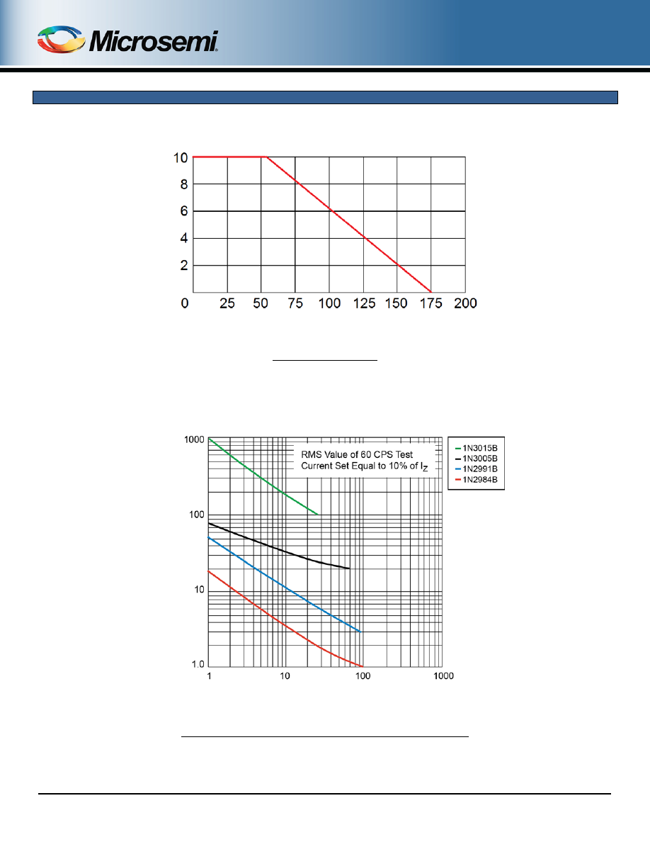
3. The Zener impedance (Z
ZT
) is derived from the 60 Hz ac voltage, which results when an ac current having an rms value equal
to 10% of the dc Zener current (I
ZT
or I
ZK
) is superimposed on I
ZT
or I
ZK
. When making Zener impedance measurements at
the I
ZK
test point, it may be necessary to insert a 60 Hz band pass filter between the diode and voltmeter to avoid errors
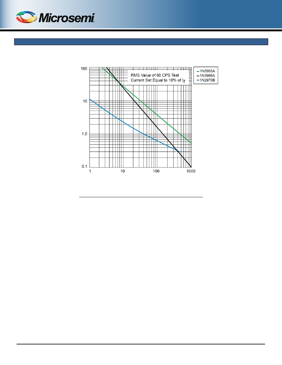
resulting from low level noise signals. A curve showing the variation of Zener impedance vs. Zener current for three
representative types is shown i
Also see Microse
4. Derate I
Z
linearly to 0.0 mA at +175 �C, for T
C
> +55 �C. These values of I
ZM
may be exceeded in the case of individual
diodes. The values shown are calculated for the worst case that is a unit of +/-5% tolerance at the high voltage end of its
tolerance range. Allowance has also been made for the rise in Zener voltage above V
ZT
, which results from Zener
impedance and the increase in junction temperature as power dissipation approaches 10 watts.
T4-LDS-0075, Rev. 3 (5/24/13)
�2013 Microsemi Corporation
Page 6 of 8
1N2970B - 1N3015B and
1N3993A - 1N3998A
GRAPHS
Case (Stud) Temperature �C
FIGURE 1
Power Derating Curve
I
ZT
Zener Current (mA)
FIGURE 2
Typical Zener Impednace vs. Zener Current for Types Shown
P
d R
at
ed
P
ow
er
D
is
s
ipat
io
n
-
W
a
tts
Z
Z
T
, Z
ener
I
mp
eda
nc
e (
O
H
MS
)
T4-LDS-0075, Rev. 3 (5/24/13)
�2013 Microsemi Corporation
Page 7 of 8
1N2970B - 1N3015B and
1N3993A - 1N3998A
GRAPHS (continued)
I
ZT
Zener Current (mA)
FIGURE 3
Typical Zener Impedance vs Zener Current for Types Shown
Z
ener
I
m
ped
anc
e (
O
H
MS
)
Z
t
T4-LDS-0075, Rev. 3 (5/24/13)
�2013 Microsemi Corporation
Page 8 of 8
1N2970B - 1N3015B and
1N3993A - 1N3998A
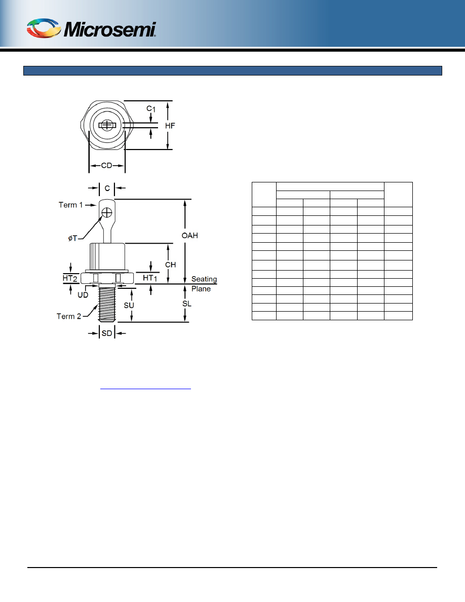
PACKAGE DIMENSIONS
NOTES:
1. Dimensions are in inches. Millimeters are given for information only.
2. See
for the polarity of the terminals.
3. Threads shall be 10-32 UNF-2A in accordance with FED-STD-H28. Maximum pitch diameter
(SD) of plated threads is 0.1697 inch (4.31 mm).
4. Maximum torque allowed on the 10-32 UNF-2B nut when assembled on the thread is 15 inch-
pounds.
5. The angular orientation and peripheral configuration of terminal 1 is undefined, however, the
major surfaces over dimension C and C1 shall be flat.
6. Dimension CD cannot exceed dimension HF.
7. A chamfer or undercut on one or both ends of the hex portion is optional; minimum base diameter
at the seating plane is 0.403 inch (10.24 mm).
8. Length of incomplete or undercut threads UD.
9.
In accordance with ASME Y14.5M, diameters are equivalent to Φx symbology.
Dimensions
Ltr
Inches
Millimeters
Notes
Min
Max
Min
Max
C
-
0.250
-
6.35
5
C1
0.012
0.065
0.30
1.65
5
CD
0.255
0.424
6.48
10.77
6
CH
0.300
0.405
7.62
10.29
HF
0.424
0.437
10.77
11.1
6
HT1
0.075
0.175
1.91
4.45
7
HT2
0.060
0.175
1.52
4.45
7
OAH
0.600
0.800
15.24
20.32
SD
-
-
-
-
2
SL
0.422
0.453
10.72
11.51
SU
-
0.078
-
1.98
UD
0.163
0.189
4.14
4.80
8
ΦT
0.060
0.095
1.52
2.41
Document Outline
- Word Bookmarks

