| Secciones |
|---|
| Foros Electrónica |
|
|
| Boletines de correo |
 |

EN - For pricing and availability in your local country please visit one of the below links:
DE - Informationen zu Preisen und Verfügbarkeit in Ihrem Land erhalten Sie über die unten aufgeführten Links:
FR - Pour connaître les tarifs et la disponibilité dans votre pays, cliquez sur l'un des liens suivants:
EN
This Datasheet is presented by
the manufacturer
DE
Dieses Datenblatt wird vom
Hersteller bereitgestellt
FR
Cette fiche technique est
présentée par le fabricant
Zener Diode
1N746A-1N759A
Page <1>
06/04/11 V1.1
http://www.element14.com
http://www.farnell.com
http://www.newark.com
Features:
High reliability.
Very sharp reverse characteristic.
Zener voltage 3.3V to 12V.
V
z
-tolerance ±5%.
Applications:
Voltage stabilization
Absolute Maximum Ratings
T
j
= 25 °C
Parameter
Test Conditions
Symbol
Value
Unit
Power dissipation
T
amb
≤ 75 °C
P
v
500
mW
Z-current
-
I
z
P
v
/V
z
mA
Junction temperature
-
T
j
200
°C
Storage temperature range
-
T
stg
-65 to +200
Maximum Thermal Resistance
T
j
= 25 °C
Parameter
Test Conditions
Symbol
Value
Unit
Junction ambient
I = 9.5mm (3/8 inches) T
L
= constant
R
thJA
300
K/W
Stresses exceeding maximum ratings may damage the device. Maximum ratings are stress ratings only. Functional
operation above the recommended operating conditions is not implied. Extended exposure to stresses above the
recommended operating conditions may affect device reliability.
Electrical Characteristics
T
j
= 25 °C
Parameter
Test Conditions
Symbol
Maximum
Unit
Forward voltage
I
F
= 200mA
V
F
1.5
V

Zener Diode
1N746A-1N759A
Page <2>
06/04/11 V1.1
http://www.element14.com
http://www.farnell.com
http://www.newark.com
Specification Table
Description
V
Znom
1)
I
ZT
for Z
ZT
I
R
at V
R
I
ZM
2)
Part Number
V
mA
Ω¦
Ω¦
µ µA
V
mA
Zener Diode
3.3
20
28
10
1
110
1N746A
Zener Diode
3.6
24
100
1N747A
Zener Diode
3.9
23
95
1N748A
Zener Diode
4.3
22
2
85
1N749A
Zener Diode
4.7
19
75
1N750A
Zener Diode
5.1
17
1
70
1N751A
Zener Diode
5.6
11
65
1N752A
Zener Diode
6.2
7
0.1
60
1N753A
Zener Diode
6.8
5
55
1N754A
Zener Diode
7.5
6
50
1N755A
Zener Diode
8.2
8
45
1N756A
Zener Diode
9.1
10
40
1N757A
Zener Diode
10
17
35
1N758A
Zener Diode
12
30
30
1N759A
1)
Tolerance and voltage designation (V
Z
)
The type numbers shown have a standard tolerance of ±5% on the nominal zener voltage, C for ±2%, D for ±1%.
2)
Maximum zener current ratings (I
ZM
)
Maximum zener current ratings are based on maximum zener voltage of the individual units and JEDEC 250 mW rating.
Zener Diode
1N746A-1N759A
Page <3>
06/04/11 V1.1
http://www.element14.com
http://www.farnell.com
http://www.newark.com
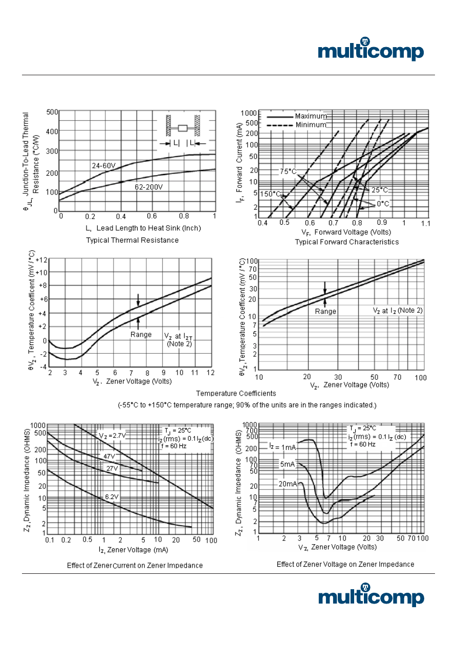
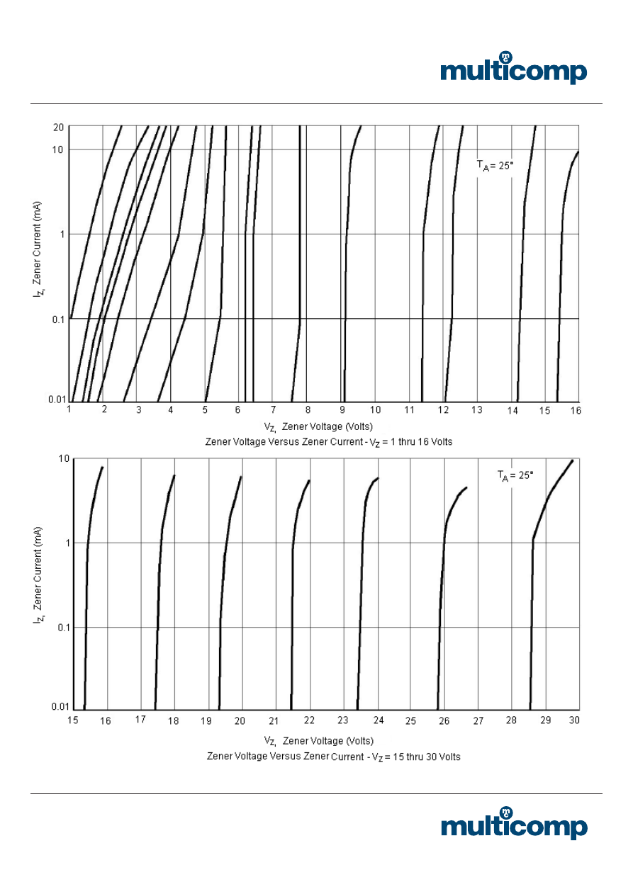
Characteristics (T
j
= 25 °C unless otherwise specified)
Zener Diode
1N746A-1N759A
Page <4>
06/04/11 V1.1
http://www.element14.com
http://www.farnell.com
http://www.newark.com

Zener Diode
1N746A-1N759A
Page <5>
06/04/11 V1.1
http://www.element14.com
http://www.farnell.com
http://www.newark.com
Important Notice : This data sheet and its contents (the "Information") belong to the members of the Premier Farnell group of companies (the "Group") or are licensed to it. No licence is granted for the use of
it other than for information purposes in connection with the products to which it relates. No licence of any intellectual property rights is granted. The Information is subject to change without notice and replaces
all data sheets previously supplied. The Information supplied is believed to be accurate but the Group assumes no responsibility for its accuracy or completeness, any error in or omission from it or for any use
made of it. Users of this data sheet should check for themselves the Information and the suitability of the products for their purpose and not make any assumptions based on information included or omitted.
Liability for loss or damage resulting from any reliance on the Information or use of it (including liability resulting from negligence or where the Group was aware of the possibility of such loss or damage arising)
is excluded. This will not operate to limit or restrict the Group's liability for death or personal injury resulting from its negligence. Multicomp is the registered trademark of the Group. © Premier Farnell plc 2011.
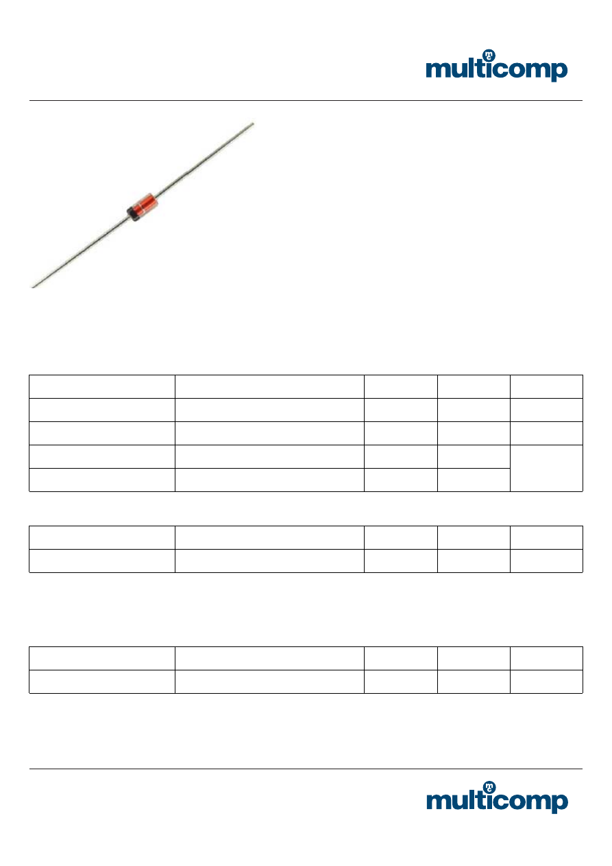
Dimensions: Millimetres
Standard Glass case
JEDEC DO-35
Marking
EN - For pricing and availability in your local country please visit one of the below links:
DE - Informationen zu Preisen und Verfügbarkeit in Ihrem Land erhalten Sie über die unten aufgeführten Links:
FR - Pour connaître les tarifs et la disponibilité dans votre pays, cliquez sur l'un des liens suivants:
EN
This Datasheet is presented by
the manufacturer
DE
Dieses Datenblatt wird vom
Hersteller bereitgestellt
FR
Cette fiche technique est
présentée par le fabricant

