| Secciones |
|---|
| Foros Electrónica |
|
|
| Boletines de correo |
 |

Atmel-8734D-SEEPROM-AT24C128C-Datasheet_082015
Features
ï¬
Low-voltage and Standard-voltage Operation
̶
V
CC
= 1.7V to 5.5V
ï¬
Internally Organized as 16,384 x 8
ï¬
2-wire Serial Interface
ï¬
Schmitt Trigger, Filtered Inputs for Noise Suppression
ï¬
Bidirectional Data Transfer Protocol
ï¬
400kHz (1.7V) and 1MHz (2.5V, 2.7V, 5.0V) Compatibility
ï¬
Write Protect Pin for Hardware Protection
ï¬
64-byte Page Write Mode
̶
Partial Page Writes Allowed
ï¬
Self-timed Write Cycle (5ms Max)
ï¬
High Reliability
̶
Endurance: 1,000,000 Write Cycles
̶
Data Retention: 40 Years
ï¬
Lead-free/Halogen-free Devices Available
ï¬
Green Package Options (Pb/Halide-free/RoHS Compliant)
̶
8-lead JEDEC SOIC, 8-lead TSSOP, 8-pad UDFN, 8-pad XDFN,
8-ball VFBGA, and 4-ball WLCSP Packages
ï¬
Die Sale Options: Wafer Form, Waffle Pack, and Bumped Wafers
Description
The Atmel
®
AT24C128C provides 131,072-bits of Serial Electrically Erasable and
Programmable Read-Only Memory (EEPROM) organized as 16,384 words of
8 bits each. The devices cascading feature allows up to eight devices to share a
common 2-wire bus. The device is optimized for use in many industrial and
commercial applications where low-power and low-voltage operation are
essential. The devices are available in space-saving 8-lead JEDEC SOIC, 8-lead
TSSOP, 8-pad UDFN, 8-pad XDFN, 8-ball VFBGA, and 4-ball WLCSP packages.
In addition, this device operates from 1.7V to 5.5V.
AT24C128C
I
2
C-Compatible (2-Wire) Serial EEPROM
128-Kbit (16,384 x 8)
DATASHEET
AT24C128C [DATASHEET]
Atmel-8734D-SEEPROM-AT24C128C-Datasheet_082015
2
1.
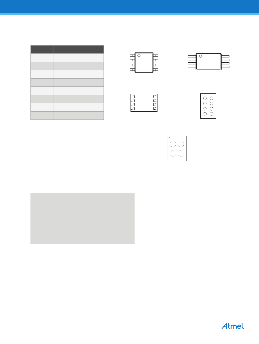
Pin Configurations and Pinouts
Table 1-1.
Pin Configuration
2.
Absolute Maximum Ratings*
Pin
Function
A
0
Address Input
A
1
Address Input
A
2
Address Input
GND
Ground
SDA
Serial Data
SCL
Serial Clock Input
WP
Write Protect
V
CC
Device Power Supply
8-lead TSSOP
Top View
1
2
3
4
8
7
6
5
A
0
A
1
A
2
GND
V
CC
WP
SCL
SDA
1
2
3
4
A
0
A
1
A
2
GND
8
7
6
5
V
CC
WP
SCL
SDA
8-lead SOIC
Top View
1
2
3
4
A
0
A
1
A
2
GND
8
7
6
5
V
CC
WP
SCL
SDA
8-pad UDFN/XDFN
Top View
A
0
A
1
A
2
GND
VCC
WP
SCL
SDA
1
2
3
4
8
7
6
5
8-ball VFBGA
Top View
V
CC
SCL
SDA
GND
4-ball WLCSP
Top View
Operating Temperature . . . . . . . . . . .-55 °C to +125 °C
Storage Temperature . . . . . . . . . . . -65 °C to + 150 °C
Voltage on any pin
with respect to ground . . . . . . . . . . . . . . . -1.0 V +7.0V
Maximum Operating Voltage . . . . . . . . . . . . . . . 6.25V
DC Output Current . . . . . . . . . . . . . . . . . . . . . . .5.0mA
*Notice: Stresses beyond those listed under Absolute
Maximum Ratings may cause permanent damage
to the device. This is a stress rating only and
functional operation of the device at these or any
other conditions beyond those indicated in the
operational sections of this specification are not
implied. Exposure to absolute maximum rating
conditions for extended periods may affect device
reliability.
3
AT24C128C [DATASHEET]
Atmel-8734D-SEEPROM-AT24C128C-Datasheet_082015
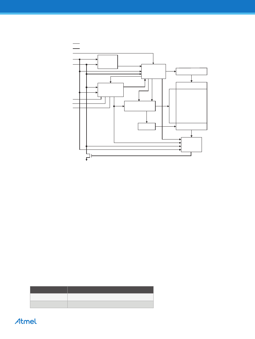
3.
Block Diagram
Figure 3-1.
Block Diagram
4.
Pin Descriptions
Serial Clock (SCL): The SCL input is used to positive-edge clock data into each EEPROM device and negative-
edge clock data out of each device.
Serial Data (SDA): The SDA pin is bidirectional for serial data transfer. This pin is open drain driven and may be
wire-ORed with any number of other open-drain or open-collector devices.
Device Addresses (A
2
, A
1
, A
0
): The A
2
, A
1
, and A
0
pins are device address inputs that are hard wired (directly to
GND or to V
CC
) for compatibility with other Atmel AT24C devices. When the pins are hard wired, as many as eight
128K devices may be addressed on a single bus system. (Device addressing is discussed in detail in
If these pins are left floating, the A
2
, A
1
, and A
0
pins will be internally pulled down to GND. However, due to
capacitive coupling that may appear during customer applications, Atmel recommends always connecting the
address pins to a known state. When using a pull-up resistor, Atmel recommends using 10k
Ω or less.
Write Protect (WP): The Write Protect input, when connected to GND, allows normal write operations. When WP
is connected directly to V
CC
, all write operations to the memory are inhibited. If the pin is left floating, the WP pin
will be internally pulled down to GND. However, due to capacitive coupling that may appear during customer
applications, Atmel recommends always connecting the WP pins to a known state. When using a pull-up resistor,
Atmel recommends using 10k
Ω or less.
Table 4-1.
Write Protect
V
CC
GND
WP
SCL
SDA
A
2
A
1
A
0
EN
EEPROM
XD
E
C
D
OUT
/ACK
LOGIC
COMP
LOAD
INC
Y DEC
R/W
D
OUT
D
IN
LOAD
Start
Stop
Logic
Serial
Control
Logic
H.V. Pump/Timing
Device
Address
Comparator
Data Word
Addr/Counter
Data Recovery
Serial MUX
WP Pin Status
Part of the Array Protected
At V
CC
Full Array
At GND
Normal Read/Write Operations
AT24C128C [DATASHEET]
Atmel-8734D-SEEPROM-AT24C128C-Datasheet_082015
4
5.
Memory Organization
AT24C128C, 128K Serial EEPROM: The 128K is internally organized as 256 pages of 64-bytes each. Random
word addressing requires a 14-bit data word address.
5.1
Pin Capacitance
Table 5-1.
Pin Capacitance
Note:
1.
This parameter is characterized and is not 100% tested.
5.2
DC Characteristics
Table 5-2.
DC Characteristics
Note:
1.
V
IL
min and V
IH
max are reference only and are not tested.
Applicable over recommended operating range from: T
A
= 25 °C, f = 1.0MHz, V
CC
= 1.7V to 5.5V.
Symbol
Test Condition
Max
Units
Conditions
C
I/O
Input/Output Capacitance (SDA)
8
pF
V
I/O
= 0V
C
IN
Input Capacitance (A
0
, A
1
, A
2
, and SCL)
6
pF
V
IN
= 0V
Applicable over recommended operating range from: T
AI
= -40 °C to +85 °C, V
CC
= 1.7V to 5.5V
(unless otherwise noted)
.
Symbol
Parameter
Test Condition
Min
Typ
Max
Units
V
CC1
Supply Voltage
1.7
5.5
V
I
CC1
Supply Current
V
CC
= 5.0V
Read at 400kHz
1.0
2.0
mA
I
CC2
Supply Current
V
CC
= 5.0V
Write at 400kHz
2.0
3.0
mA
I
SB1
Standby Current
V
CC
= 1.7V
V
IN
= V
CC
or V
SS
1.0
µA
V
CC
= 5.0V
6.0
µA
I
LI
Input Leakage
Current V
CC
= 5.0V
V
IN
= V
CC
or V
SS
0.10
3.0
µA
I
LO
Output Leakage
Current V
CC
= 5.0V
V
OUT
= V
CC
or V
SS
0.05
3.0
µA
V
IL
Input Low Level
-0.6
V
CC
x 0.3
V
V
IH
Input High Level
(
V
CC
x 0.7
V
CC
+ 0.5
V
V
OL1
Output Low Level
V
CC
= 1.7V
I
OL
= 0.15mA
0.2
V
V
OL2
Output Low Level
V
CC
= 3.0V
I
OL
= 2.1mA
0.4
V
5
AT24C128C [DATASHEET]
Atmel-8734D-SEEPROM-AT24C128C-Datasheet_082015
5.3
AC Characteristics
Table 5-3.
AC Characteristics (Industrial Temperature)
Notes: 1.
This parameter is ensured by characterization and is not 100% tested.
2.
AC measurement conditions:
ï¬
R
L
(connects to V
CC
): 1.3kΩ (2.5V, 5.5V), 10kΩ (1.7V)
ï¬
Input pulse voltages: 0.3V
CC
to 0.7V
CC
ï¬
Input rise and fall times: ≤ 50ns
ï¬
Input and output timing reference voltages: 0.5 x V
CC
Applicable over recommended operating range from: T
AI
= -40 °C to +85 °C, V
CC
= 1.7V to 5.5V, CL = 100pF (unless
otherwise noted). Test conditions are listed in
Symbol
Parameter
1.7V
2.5V, 5.0V
Units
Min
Max
Min
Max
f
SCL
Clock Frequency, SCL
400
1000
kHz
t
LOW
Clock Pulse Width Low
1300
400
ns
t
HIGH
Clock Pulse Width High
600
400
ns
t
I
100
50
ns
t
AA
Clock Low to Data Out Valid
50
900
50
550
ns
t
BUF
Time the bus must be free before a new transmission
can start
1300
500
ns
t
HD.STA
Start Hold Time
600
250
ns
t
SU.STA
Start Set-up Time
600
250
ns
t
HD.DAT
Data In Hold Time
0
0
ns
t
SU.DAT
Data In Set-up Time
100
100
ns
t
R
Inputs Rise Time
300
300
ns
t
F
300
100
ns
t
SU.STO
Stop Set-up Time
600
250
ns
t
DH
Data Out Hold Time
50
50
ns
t
WR
Write Cycle Time
5
5
ms
Endurance
25 °C, Page Mode, 3.3V
1,000,000
Write Cycles
AT24C128C [DATASHEET]
Atmel-8734D-SEEPROM-AT24C128C-Datasheet_082015
6
6.
Device Operation
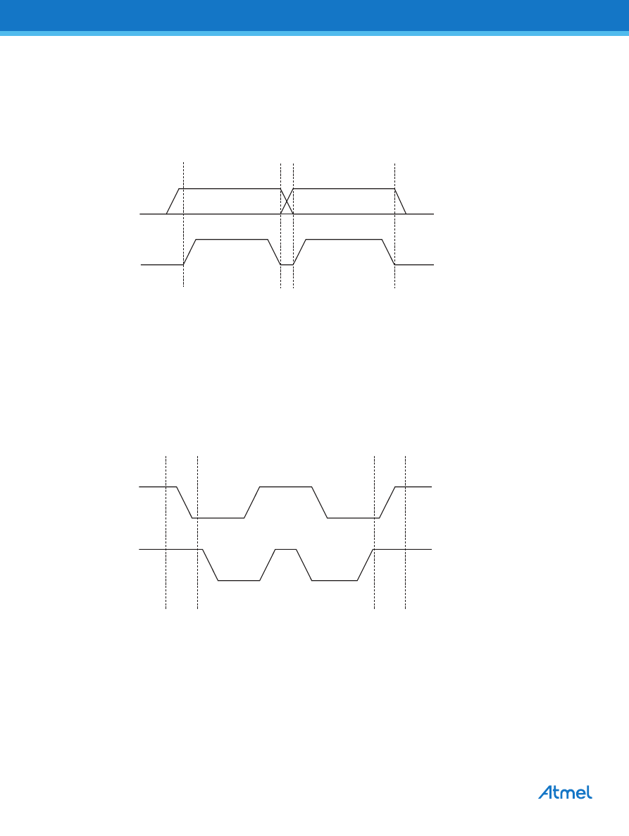
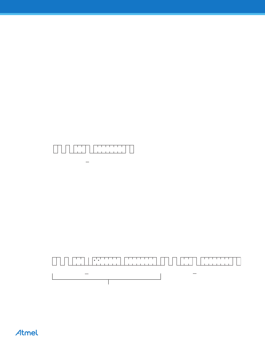
Clock and Data Transitions: The SDA pin is normally pulled high with an external device. Data on the SDA pin
may change only during SCL low time periods. Data changes during SCL high periods will indicate a start or
stop condition as defined below.
Figure 6-1.
Data Validity
Start Condition: A high-to-low transition of SDA with SCL high is a start condition that must precede any other
command.
Stop Condition: A low-to-high transition of SDA with SCL high is a stop condition. After a read sequence, the
stop command will place the EEPROM in a standby power mode.
Figure 6-2.
Start and Stop Definition
SDA
SCL
Data
Change
Data Stable
Data Stable
SDA
SCL
Start
Stop
7
AT24C128C [DATASHEET]
Atmel-8734D-SEEPROM-AT24C128C-Datasheet_082015
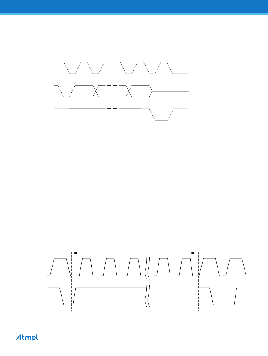
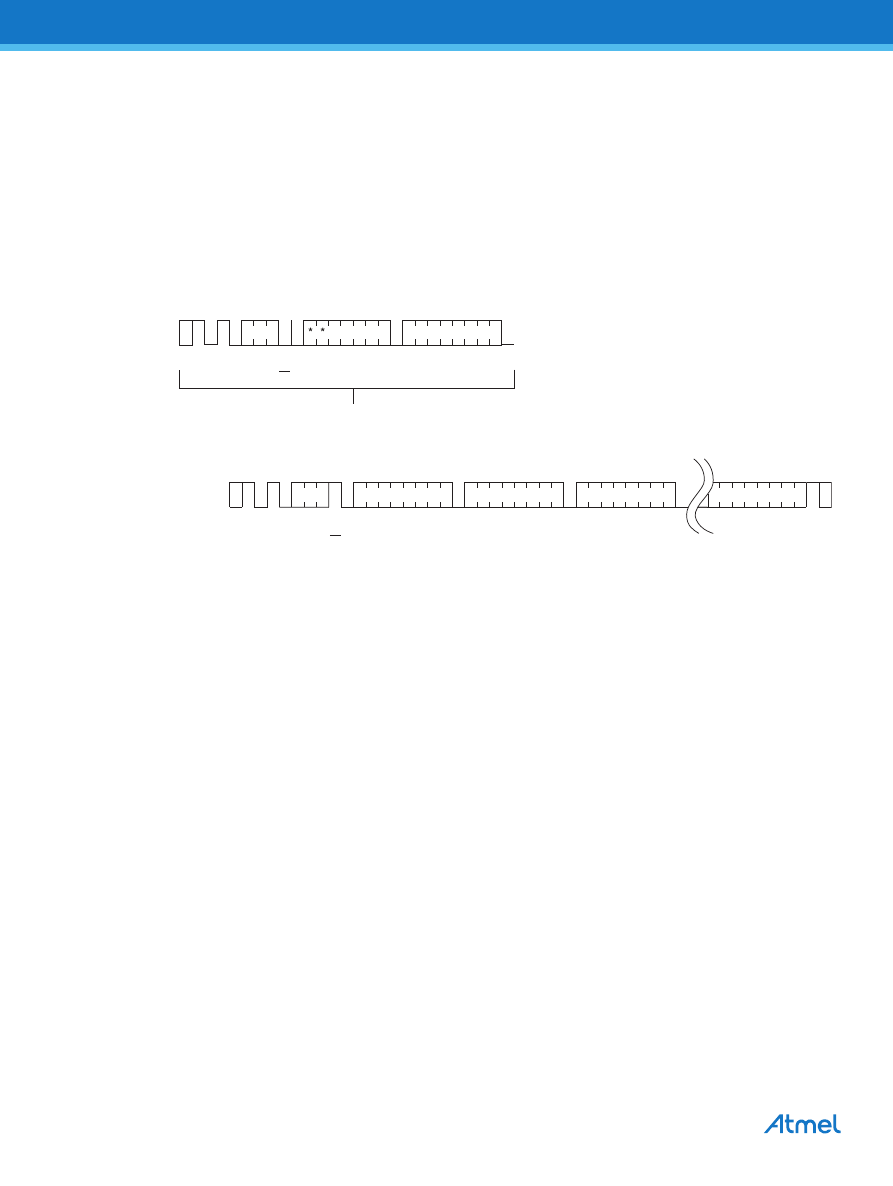
Acknowledge: All addresses and data words are serially transmitted to and from the EEPROM in 8-bit words.
The EEPROM sends a zero during the ninth clock cycle to acknowledge that it has received each word.
Figure 6-3.
Output Acknowledge
Standby Mode: AT24C128C features a low-power standby mode that is enabled upon power-up and after the
receipt of the stop bit and the completion of any internal operations.
Software Reset: After an interruption in protocol, power loss or system reset, any 2-wire part can be protocol
reset by following these steps:
1.
Create a Start condition (if possible).
2.
Clock nine cycles.
3.
Create another Start condition followed by Stop condition as shown below.
The device should be ready for the next communication after above steps have been completed. In the event
that the device is still non-responsive or remains active on the SDA bus, a power cycle must be used to reset
the device.
Figure 6-4.
Software Reset
SCL
Data In
Data Out
Start
Acknowledge
9
8
1
SCL
9
Start
Condition
Start
Condition
Stop
Condition
8
3
2
1
SDA
Dummy Clock Cycles
AT24C128C [DATASHEET]
Atmel-8734D-SEEPROM-AT24C128C-Datasheet_082015
8
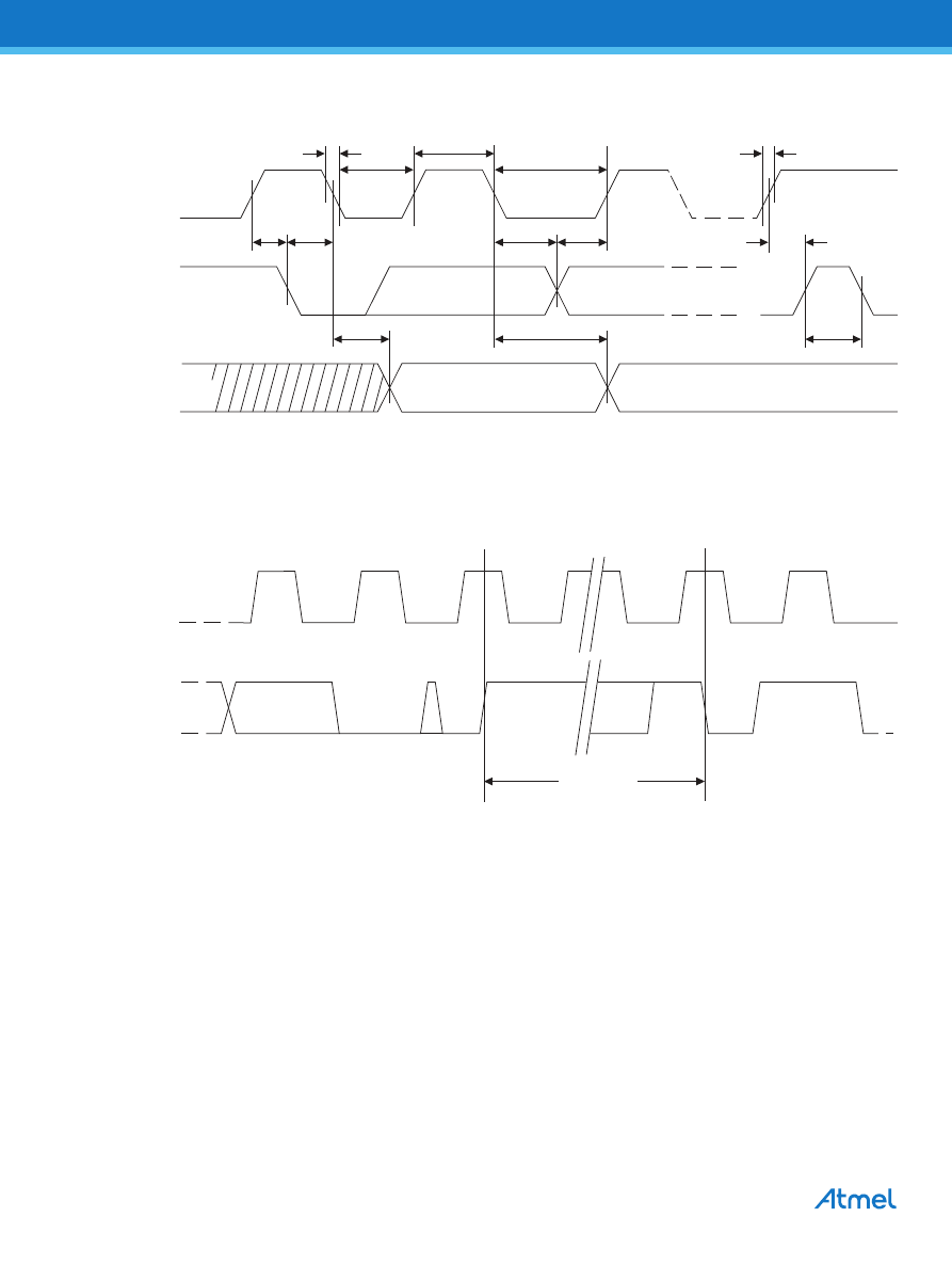
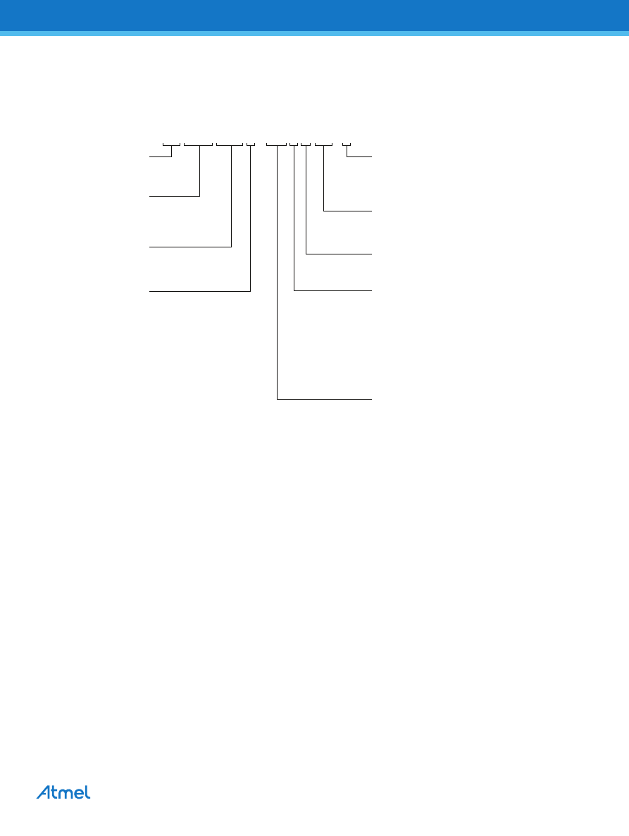
Figure 6-5.
Bus Timing
Figure 6-6.
Write Cycle Timing
Note:
1.
The write cycle time t
WR
is the time from a valid stop condition of a write sequence to the end of
the internal clear/write cycle.
SCL
SDA In
SDA Out
t
F
t
HIGH
t
LOW
t
LOW
t
R
t
AA
t
DH
t
BUF
t
SU.STO
t
SU.DAT
t
HD.DAT
t
HD.STA
t
SU.STA
SCL
SDA
t
WR
(1)
Stop
Condition
Start
Condition
WORD
N
ACK
8
th
Bit
9
AT24C128C [DATASHEET]
Atmel-8734D-SEEPROM-AT24C128C-Datasheet_082015
7.
Device Addressing
The 128K EEPROM requires an 8-bit device address word following a start condition to enable the chip for a
read or write operation. The device address word consists of a mandatory one, zero sequence for the first four
most significant bits as shown. This is common to all 2-wire EEPROM devices.
Table 7-1.
Device Address Byte
The next three bits are the A2, A1, and A0 device address bits to allow as many as eight devices on the same
bus. These bits must compare to their corresponding hard wired input pins. The A
2
, A
1
, and A
0
pins use an
internal proprietary circuit that biases them to a logic low condition if the pins are allowed to float.
When using the WLCSP package, the A
2
, A
1
, and A
0
signals are not accessible. The A
2
and A
1
pins are left
floating, and the previously mentioned automatic pull-down circuit will set these signals to a Logic 0 state. The
A
0
signal is internally connected to V
CC
. As a result, to properly communicate with the device in the WLCSP
package, the A2 and A1 software bits must always be set to a Logic 0, and the A0 software bit must be set to
Logic 1 for any operation. This requirement has been shown in
The eighth bit of the device address is the read/write operation select bit. A read operation is initiated if this bit is
high, and a write operation is initiated if this bit is low.
Upon a compare of the device address, the EEPROM will output a zero. If a compare is not made, the device
will return to a standby state.
Data Security: AT24C128C has a hardware data protection scheme that allows the user to write protect the
whole memory when the WP pin is at V
CC
.
Package
Device Type Identifier
Hardware Slave Address Bits
Read/ Write
Bit 7
Bit 6
Bit 5
Bit 4
Bit 3
Bit 2
Bit 1
Bit 0
SOIC, TSSOP, UDFN,
XDFN, VFBGA
1
0
1
0
A
2
A
1
A
0
R/W
WLCSP
1
0
1
0
0
0
1
R/W

AT24C128C [DATASHEET]
Atmel-8734D-SEEPROM-AT24C128C-Datasheet_082015
10
8.
Write Operations
Byte Write: A write operation requires two 8-bit data word addresses following the device address word and
acknowledgment. Upon receipt of this address, the EEPROM will again respond with a zero, and then clock in
the first 8-bit data word. Following receipt of the 8-bit data word, the EEPROM will output a zero. The
addressing device, such as a microcontroller, must then terminate the write sequence with a stop condition. At
this time, the EEPROM enters an internally-timed write cycle, t
WR
, to the nonvolatile memory. All inputs are
disabled during this write cycle and the EEPROM will not respond until the write is complete.
Figure 8-1.
Byte Write
Note:
* = Dont care bit
Page Write: The 128K EEPROM is capable of 64-byte page writes.
A page write is initiated the same way as a byte write, but the microcontroller does not send a stop condition
after the first data word is clocked in. Instead, after the EEPROM acknowledges receipt of the first data word,
the microcontroller can transmit up to 63 more data words. The EEPROM will respond with a zero after each
data word received. The microcontroller must terminate the page write sequence with a stop condition.
Figure 8-2.
Page Write
Note:
* = Dont care bit
The data word address lower six bits are internally incremented following the receipt of each data word. The
higher data word address bits are not incremented, retaining the memory page row location. When the word
address, internally generated, reaches the page boundary, the following byte is placed at the beginning of the
same page. If more than 64 data words are transmitted to the EEPROM, the data word address will roll-over
and the previous data will be overwritten. The address roll-over during write is from the last byte of the current
page to the first byte of the same page.
Acknowledge Polling: Once the internally-timed write cycle has started and the EEPROM inputs are disabled,
acknowledge polling can be initiated. This involves sending a start condition followed by the device address
word. The read/write bit is representative of the operation desired. Only if the internal write cycle has completed
will the EEPROM respond with a zero, allowing the read or write sequence to continue.
S
T
A
R
T
W
R
I
T
E
S
T
O
P
Device
Address
First
Word Address
Second
Word Address
Data
SDA Line
M
S
B
A
C
K
R
/
W
A
C
K
A
C
K
A
C
K
SDA Line
S
T
A
R
T
W
R
I
T
E
Device
Address
First
Word Address
Second
Word Address
Data (n)
Data (n + x)
M
S
B
A
C
K
R
/
W
A
C
K
A
C
K
A
C
K
A
C
K
S
T
O
P
11
AT24C128C [DATASHEET]
Atmel-8734D-SEEPROM-AT24C128C-Datasheet_082015
9.
Read Operations
Read operations are initiated the same way as write operations with the exception that the read/write select bit
in the device address word is set to one. There are three read operations:
ï¬
Current Address Read
ï¬
Random Address Read
ï¬
Sequential Read
Current Address Read: The internal data word address counter maintains the last address accessed during
the last read or write operation, incremented by one. This address stays valid between operations as long as the
chip power is maintained. The address roll-over during read is from the last byte of the last memory page, to the
first byte of the first page.
Once the device address with the read/write select bit set to one is clocked in and acknowledged by the
EEPROM, the current address data word is serially clocked out. The microcontroller does not respond with an
input zero but does generate a following stop condition.
Figure 9-1.
Current Address Read
Random Read: A Random Read requires a dummy byte write sequence to load in the data word address. Once
the device address word and data word address are clocked in and acknowledged by the EEPROM, the
microcontroller must generate another start condition. The microcontroller now initiates a Current Address Read
by sending a device address with the read/write select bit high. The EEPROM acknowledges the device
address and serially clocks out the data word. The microcontroller does not respond with a zero but does
generate a following stop condition.
Figure 9-2.
Random Read
Note:
* = Dont care bit
SDA Line
S
T
A
R
T
Device
Address
R
E
A
D
S
T
O
P
M
S
B
A
C
K
R
/
W
N
O
A
C
K
Data
SDA LINE
S
T
A
R
T
S
T
A
R
T
R
E
A
D
W
R
I
T
E
S
T
O
P
Device
Address
Second Word
Address
Device
Address
First Word
Address
Data (n)
M
S
B
A
C
K
A
C
K
A
C
K
L
S
B
A
C
K
N
O
A
C
K
R
/
W
Dummy Write
R
/
W
AT24C128C [DATASHEET]
Atmel-8734D-SEEPROM-AT24C128C-Datasheet_082015
12
Sequential Read: Sequential Reads are initiated by either a Current Address Read or a Random Address
Read. After the microcontroller receives a data word, it responds with an acknowledge. As long as the EEPROM
receives an acknowledge, it will continue to increment the data word address and serially clock out sequential
data words. When the memory address maximum address is reached, the data word address will roll-over and
the Sequential Read will continue from the beginning of the array. The Sequential Read operation is terminated
when the microcontroller does not respond with a zero but does generate a following stop condition.
Figure 9-3.
Sequential Read
Note:
* = Dont care bit
SDA LINE
S
T
A
R
T
S
T
A
R
T
R
E
A
D
W
R
I
T
E
S
T
O
P
Device
Address
Second Word
Address
Device
Address
First Word
Address
Data (n + 1)
Data (n + 2)
Data (n + x)
Data (n)
M
S
B
A
C
K
A
C
K
A
C
K
L
S
B
A
C
K
A
C
K
A
C
K
A
C
K
N
O
A
C
K
R
/
W
Dummy Write
. . .
. . .
R
/
W
13
AT24C128C [DATASHEET]
Atmel-8734D-SEEPROM-AT24C128C-Datasheet_082015
10.
Ordering Information
10.1 Ordering Code Detail
Atmel Designator
Product Family
Device Density
Device Revision
Shipping Carrier Option
Operating Voltage
Package Option
128 = 128K
24C = Standard I
2
C
Serial EEPROM
B = Bulk (Tubes)
T = Tape and Reel, Standard Quantity Option
E = Tape and Reel, Expanded Quantity Option
Product Variation
xx = A
pplies to select packages only.
See ordering code table for variation details.
M = 1.7V to 5.5V
SS
= JEDEC SOIC
X =
TSSOP
MA
= UDFN
ME
= XDFN
C =
VFBGA
U =
WLCSP
WWU = Wafer Unsawn
WDT = Die in Tape and Reel
Package Device Grade or
Wafer/Die Thickness
H = Green, NiPdAu Lead Finish,
Industrial Temperature Range
(-40 °C to +85 °C)
U = Green, Matte Sn Lead Finish,
Industrial Temperature Range
(-40 °C to +85 °C)
11 = 11mil wafer thickness
A T 2 4 C 1 2 8 C - S S H M x x - B
AT24C128C [DATASHEET]
Atmel-8734D-SEEPROM-AT24C128C-Datasheet_082015
14
10.2 Ordering Code Information
Notes: 1. WLCSP Package:
ï¬
This device includes a backside coating to increase product robustness.
ï¬
CAUTION
: Exposure to ultraviolet (UV) light can degrade the data stored in the EEPROM cells. Therefore,
customers who use a WLCSP product must ensure that exposure to ultraviolet light
does not occur.
2. Contact Atmel Sales for Wafer sales.
Atmel Ordering Code
Lead Finish
Package
Delivery Information
Operating
Range
Form
Quantity
AT24C128C-SSHM-B
NiPdAu
(Lead-free/Halogen-free)
8S1
Bulk (Tubes)
100 per Tube
Industrial
Temperature
(-40 °C to 85 °C)
AT24C128C-SSHM-T
Tape and Reel
4,000 per Reel
AT24C128C-XHM-B
8X
Bulk (Tubes)
100 per Tube
AT24C128C-XHM-T
Tape and Reel
5,000 per Reel
AT24C128C-MAHM-T
8MA2
Tape and Reel
5,000 per Reel
AT24C128C-MAHM-E
15,000 per Reel
AT24C128C-MAHMML-T
5,000 per Reel
AT24C128C-MEHM-T
8ME1
Tape and Reel
5,000 per Reel
AT24C128C-CUM-T
SnAgCu Ball
(Lead-free/Halogen-free)
8U2-1
Tape and Reel
5,000 per Reel
AT24C128C-UUM0B-T
4U-9
Tape and Reel
5,000 per Reel
AT24C128C-WWU11M
N/A
Wafer Sale
Package Type
8S1
8-lead, 0.150 wide, Plastic Gull Wing Small Outline (JEDEC SOIC)
8X
8-lead, 4.40mm body, Plastic Thin Shrink Small Outline Package (TSSOP)
8MA2
8-pad, 2.00mm x 3.00mm body, 0.50mm pitch, Dual No Lead (UDFN)
8ME1
8-pad, 1.80mm x 2.20mm body, Extra Thin DFN (XDFN)
8U2-1
8-ball, Die Ball Grid Array (VFBGA)
4U-9
4-ball, 2 x 2 Grid Array, 0.40mm minimum pitch, Wafer Level Chip Scale Package (WLCSP)

15
AT24C128C [DATASHEET]
Atmel-8734D-SEEPROM-AT24C128C-Datasheet_082015
11.
Part Markings
DRAWING NO.
REV.
TITLE
24C128CSM
D
1/5/15
24C128CSM, AT24C128C Standard Package Marking
Information
Package Mark Contact:
DL-CSO-Assy_eng@atmel.com
AAAAAAAA
###% @
ATMLHYWW
8-lead SOIC
8-lead TSSOP
AAAAAAA
###% @
ATHYWW
###
YXX
8-lead XDFN
8-lead UDFN
###
H%@
YXX
2.0 x 3.0 mm Body
1.8 x 2.2 mm Body
Note 2: Package drawings are not to scale
Note 1: designates pin 1
AT24C128C: Package Marking Information
###U
@YMXX
2.35 x 3.73 mm Body
8-ball VFBGA
Catalog Number Truncation
AT24C128C
Truncation Code ###: 2DC
Date
Codes
Voltages
Y = Year
M = Month
WW = Work Week of Assembly
% = Minimum Voltage
5: 2015
9: 2019
A: January
02: Week 2
M: 1.7V min
6: 2016
0: 2020
B: February
04: Week 4
7: 2017
1: 2021
...
...
8: 2018
2: 2022
L: December
52: Week 52
Country of Assembly
Lot Number
Grade/Lead Finish Material
@ = Country of Assembly
AAA...A = Atmel Wafer Lot Number
U: Industrial/Matte Tin
H: Industrial/NiPdAu
Trace
Code
Atmel Truncation
XX = Trace Code (Atmel Lot Numbers Correspond to Code)
AT: Atmel
Example: AA, AB.... YZ, ZZ
ATM: Atmel
ATML: Atmel
###U
YMXX
4-ball WLCSP
AT24C128C [DATASHEET]
Atmel-8734D-SEEPROM-AT24C128C-Datasheet_082015
16
12.
Packaging Information
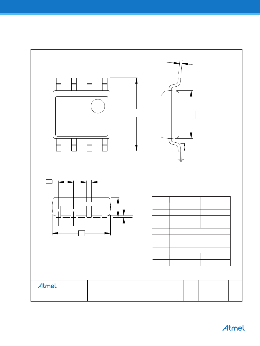
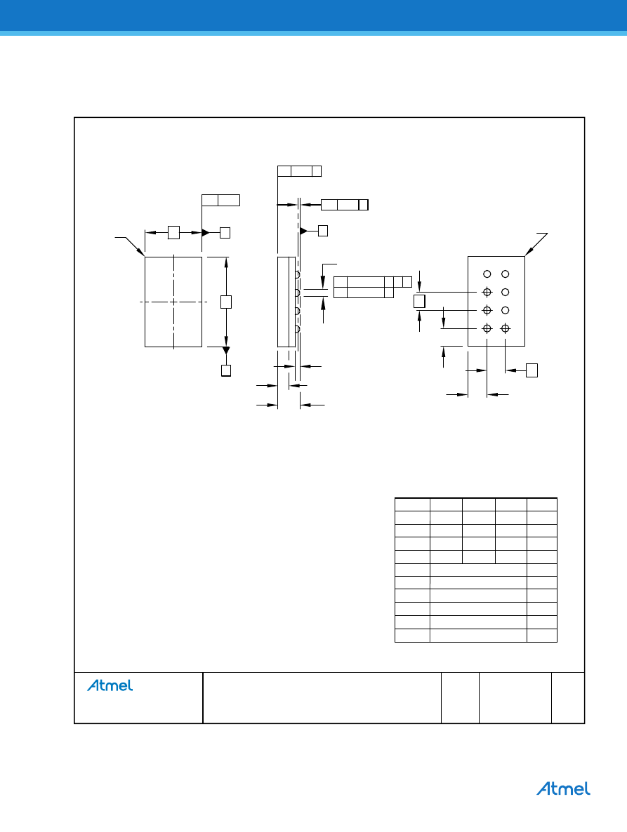
12.1 8S1 8-lead JEDEC SOIC
DRAWING NO.
REV.
TITLE
GPC
COMMON DIMENSIONS
(Unit of Measure = mm)
SYMBOL
MIN
NOM
MAX
NOTE
A1
0.10
-
0.25
A
-
-
1.75
b 0.31 - 0.51
C
0.17
-
0.25
D
4.90 BSC
E
6.00 BSC
E1
3.90 BSC
e
1.27 BSC
L 0.40 - 1.27
Ã
Ã
0 ° - 8 °
Ã
E
1
N
TOP VIEW
C
E1
END VIEW
A
b
L
A1
e
D
SIDE VIEW
Package Drawing Contact:
packagedrawings@atmel.com
8S1
H
3/6/2015
Notes: This drawing is for general information only.
Refer to JEDEC Drawing MS-012, Variation AA
for proper dimensions, tolerances, datums, etc.
8S1, 8-lead (0.150 Wide Body), Plastic Gull Wing
Small Outline (JEDEC SOIC)
SWB
17
AT24C128C [DATASHEET]
Atmel-8734D-SEEPROM-AT24C128C-Datasheet_082015
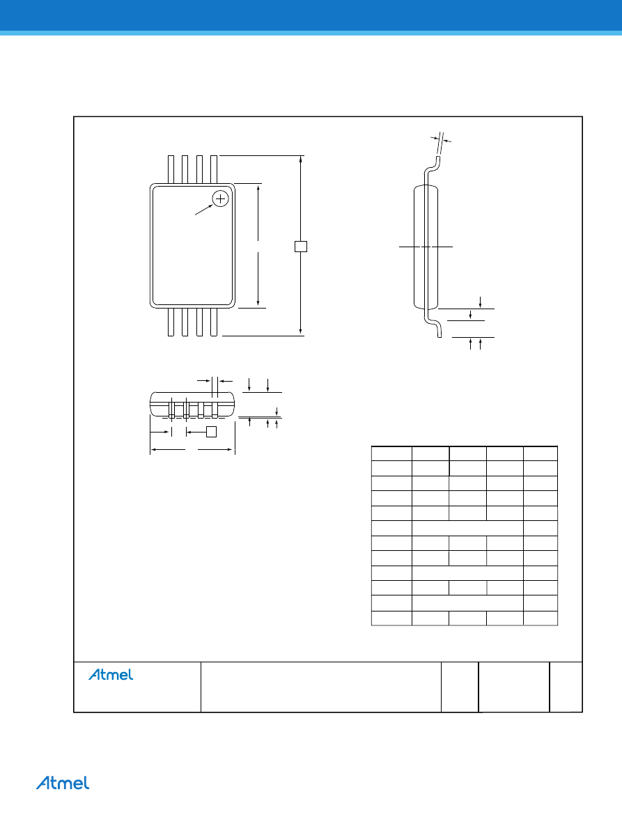
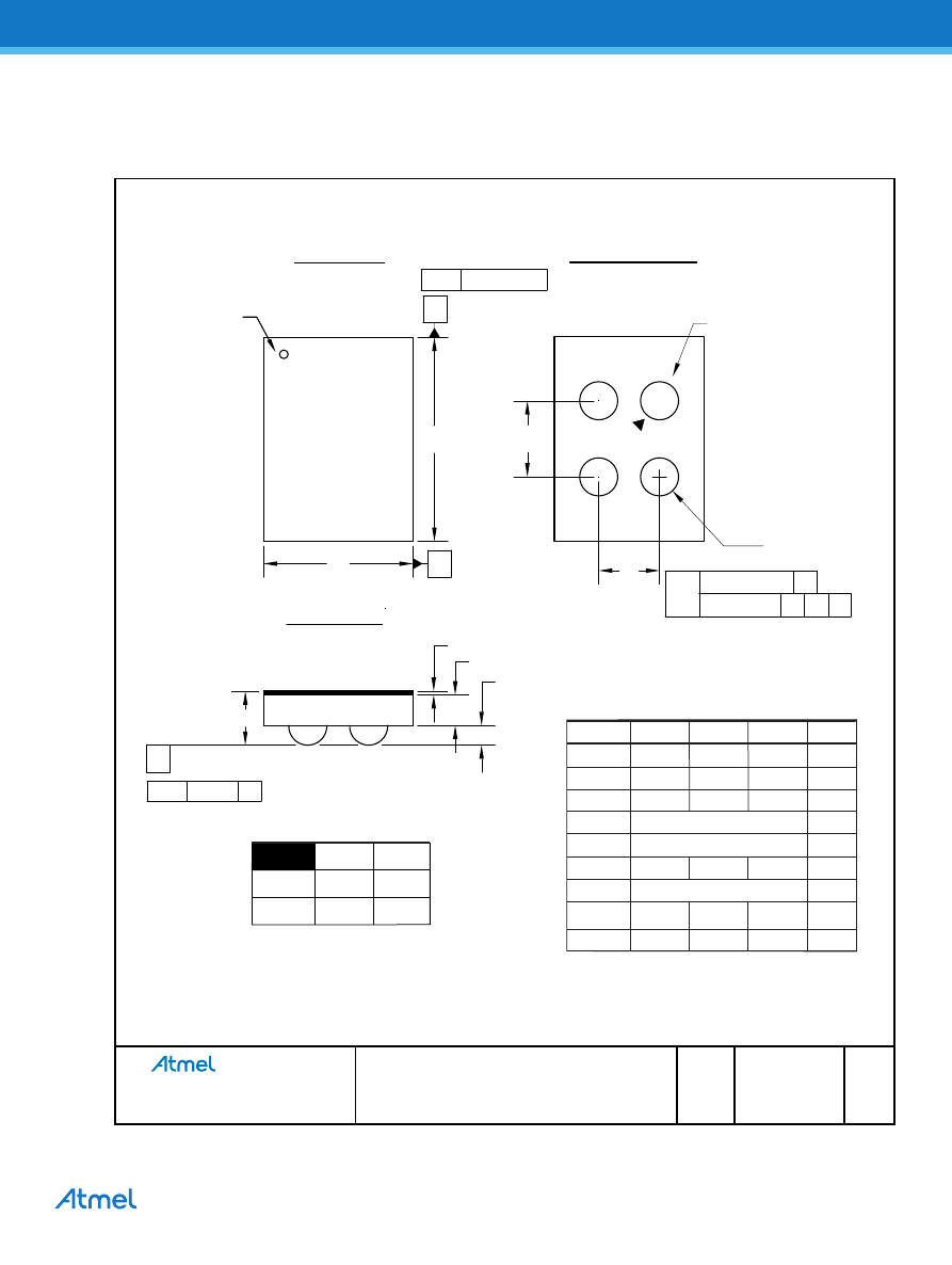
12.2 8X 8-lead TSSOP
DRAWING NO.
REV.
TITLE
GPC
COMMON DIMENSIONS
(Unit of Measure = mm)
SYMBOL
MIN
NOM
MAX
NOTE
A - -
1.20
A1 0.05 - 0.15
A2 0.80
1.00
1.05
D 2.90
3.00
3.10
2,
5
E
6.40
BSC
E1 4.30
4.40
4.50
3,
5
b
0.19
0.25
0.30
4
e
0.65 BSC
L
0.45
0.60
0.75
L1
1.00
REF
C 0.09 -
0.20
Side View
End View
Top View
A2
A
L
L1
D
1
E1
N
b
Pin 1 indicator
this corner
E
e
Notes:
1. This drawing is for general information only.
Refer to JEDEC Drawing MO-153, Variation AA, for proper
dimensions, tolerances, datums, etc.
2. Dimension D does not include mold Flash, protrusions or gate
burrs. Mold Flash, protrusions and gate burrs shall not exceed
0.15mm (0.006in) per side.
3. Dimension E1 does not include inter-lead Flash or protrusions.
Inter-lead Flash and protrusions shall not exceed 0.25mm
(0.010in) per side.
4. Dimension b does not include Dambar protrusion.
Allowable Dambar protrusion shall be 0.08mm total in excess
of the b dimension at maximum material condition. Dambar
cannot be located on the lower radius of the foot. Minimum
space between protrusion and adjacent lead is 0.07mm.
5. Dimension D and E1 to be determined at Datum Plane H.
Package Drawing Contact:
packagedrawings@atmel.com
8X
E
2/27/14
8X, 8-lead 4.4mm Body, Plastic Thin
Shrink Small Outline Package (TSSOP)
TNR
C
A1
AT24C128C [DATASHEET]
Atmel-8734D-SEEPROM-AT24C128C-Datasheet_082015
18
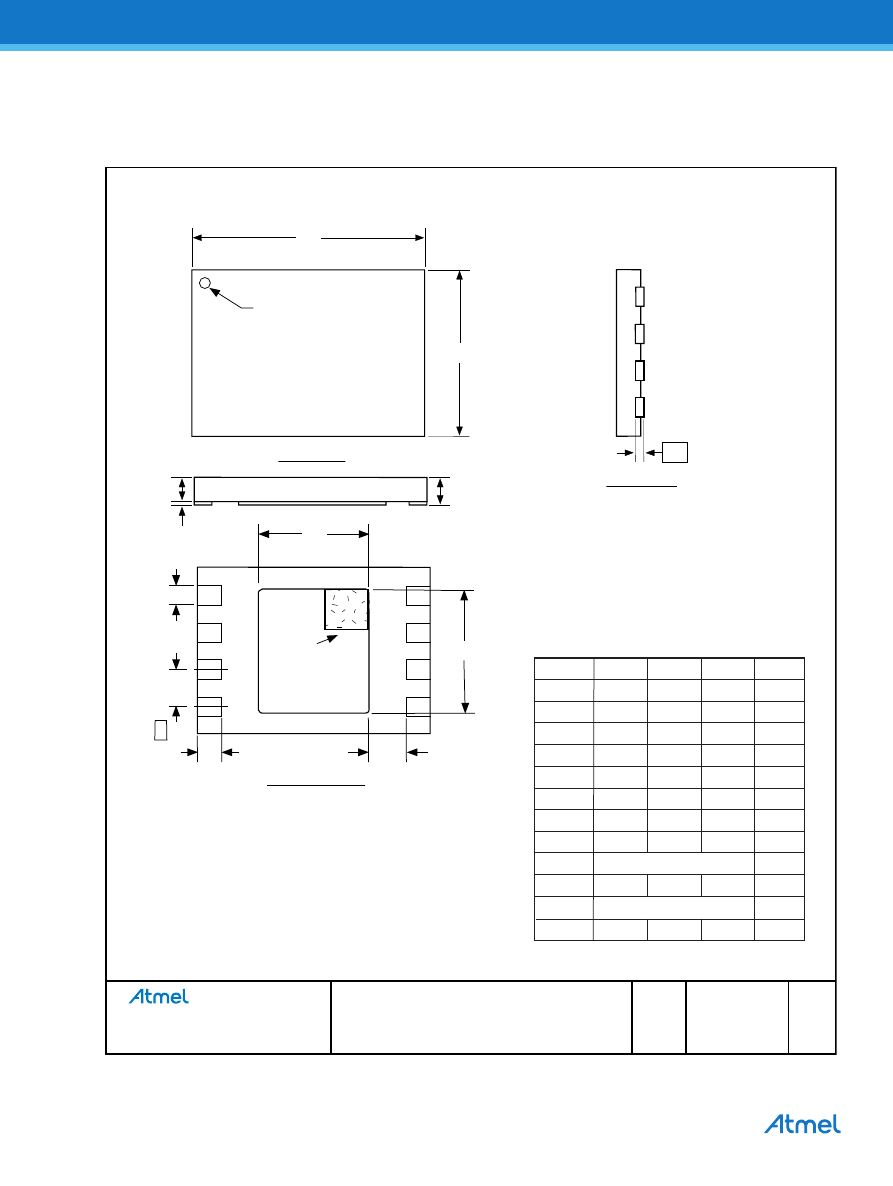
12.3 8MA2 8-pad UDFN
DRAWING NO.
REV.
TITLE
GPC
8MA2
G
11/26/14
8MA2, 8-pad 2 x 3 x 0.6mm Body, Thermally
Enhanced Plastic Ultra Thin Dual Flat No-Lead
Package (UDFN)
YNZ
COMMON DIMENSIONS
(Unit of Measure = mm)
SYMBOL
MIN
NOM
MAX
NOTE
A
0.50
0.55
0.60
A1
0.0
0.02
0.05
A2
-
-
0.55
D
1.90
2.00
2.10
D2
1.40
1.50
1.60
E
2.90
3.00
3.10
E2
1.20
1.30
1.40
b 0.18
0.25
0.30
3
C
1.52 REF
L
0.30
0.35
0.40
e
0.50 BSC
K
0.20
-
-
TOP VIEW
SIDE VIEW
BOTTOM VIEW
Package Drawing Contact:
packagedrawings@atmel.com
C
E
Pin 1 ID
D
8
7
6
5
1
2
3
4
A
A1
A2
D2
E2
e (6x)
L (8x)
b (8x)
Pin#1 ID
K
1
2
3
4
8
7
6
5
Notes:
1. This drawing is for general information only. Refer to
Drawing MO-229, for proper dimensions, tolerances,
datums, etc.
2. The Pin #1 ID is a laser-marked feature on Top View.
3. Dimensions b applies to metallized terminal and is
measured between 0.15 mm and 0.30 mm from the
terminal tip. If the terminal has the optional radius on
the other end of the terminal, the dimension should
not be measured in that radius area.
4. The Pin #1 ID on the Bottom View is an orientation
feature on the thermal pad.
19
AT24C128C [DATASHEET]
Atmel-8734D-SEEPROM-AT24C128C-Datasheet_082015
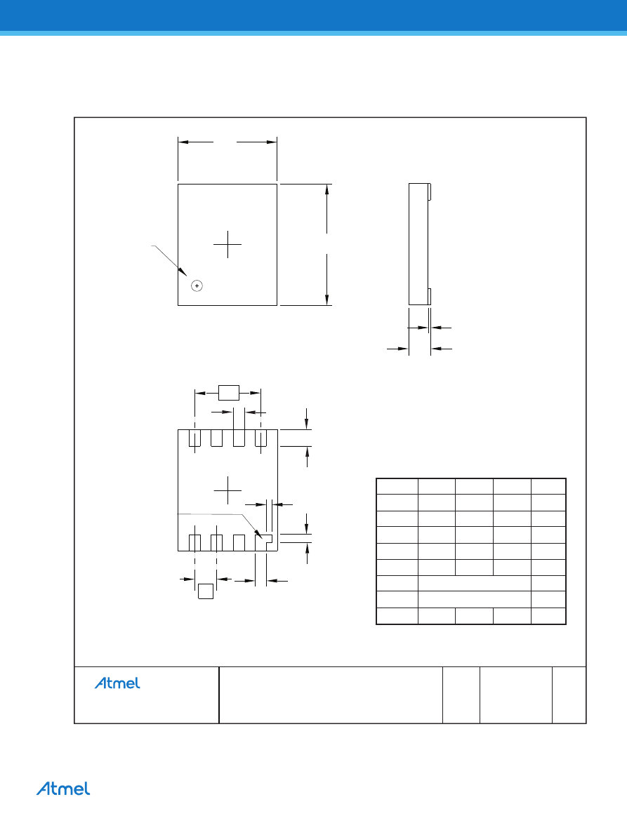
12.4 8ME1 8-pad XDFN
Package Drawing Contact:
packagedrawings@atmel.com
GPC
DRAWING NO.
REV.
TITLE
COMMON DIMENSIONS
(Unit of Measure = mm)
DTP
SYMBOL
MIN
NOM
MAX
NOTE
-
0.00
1.70
2.10
0.15
0.26
A
A1
D
E
b
e
e1
L
-
-
1.80
2.20
0.20
0.40 TYP
1.20 REF
0.30
0.40
0.05
1.90
2.30
0.25
0.35
End View
8ME1
B
9/10/2012
8ME1, 8-pad (1.80mm x 2.20mm body)
Extra Thin DFN (XDFN)
Top View
6
5
7
4
3
E
D
8
1
2
PIN #1 ID
0.10
0.15
b
L
b
e
PIN #1 ID
e1
A1
A
Side View
AT24C128C [DATASHEET]
Atmel-8734D-SEEPROM-AT24C128C-Datasheet_082015
20
12.5 8U2-1 8-ball VFBGA
DRAWING NO.
REV.
TITLE
GPC
Package Drawing Contact:
packagedrawings@atmel.com
8U2-1
G
6/11/13
8U2-1, 8-ball, 2.35 x 3.73 mm Body, 0.75 mm pitch,
Very Thin, Fine-Pitch Ball Grid Array Package
(VFBGA)
GWW
COMMON DIMENSIONS
(Unit of Measure = mm)
SYMBOL
MIN
NOM
MAX
NOTE
A
0.81 0.91 1.00
A1 0.15 0.20 0.25
A2 0.40 0.45 0.50
b
0.25 0.30 0.35
D
2.35 BSC
E
3.73 BSC
e
0.75 BSC
e1
0.74 REF
d
0.75 BSC
d1
0.80 REF
2. Dimension 'b' is measured at the maximum solder ball diameter.
1. This drawing is for general
3. Solder ball composition shall be 95.5Sn-4.0Ag-.5Cu.
Notes:
A
d 0.08 C
C
f 0.10 C
A1
A2
Ãb
j n0.15 m C A B
j n0.08 m C
A
(4X)
d 0.10
B
A1 BALL
PAD
CORNER
D
E
SIDE VIEW
TOP VIEW
e
(e1)
d
2
1
D
C
B
A
A1 BALL PAD CORNER
(d1)
8 SOLDER BALLS
BOTTOM VIEW
21
AT24C128C [DATASHEET]
Atmel-8734D-SEEPROM-AT24C128C-Datasheet_082015
12.6 4U-9 4-ball WLCSP
DRAWING NO.
REV.
TITLE
GPC
4U-9
A
12/23/14
4U-9, 4-ball 2x2 Array, 0.40/0.50mm Pitch
Wafer Level Chip-Scale Package (WLCSP) with BSC
GFC
COMMON DIMENSIONS
(Unit of Measure = mm)
SYMBOL
MIN
TYP
MAX
NOTE
A
0.260
0.295
0.330
A1
0.080
0.095
0.110
A2
0.160
0.175
0.190
A3
0.025 REF 3
D Contact Atmel for details
d1
0.400
E Contact Atmel for details
e1
0.500
b
0.170
0.185
0.200
Package Drawing Contact:
packagedrawings@atmel.com
PIN ASSIGNMENT MATRIX
1 2
A
B
SCL
GND
V
CC
SDA
TOP VIEW
SIDE VIEW
BOTTOM SIDE
D
E
A
A1
A2
A3
d1
e1
d
0.015
m
C
v
0.05
C A B
B
C
k
0.015 (4X)
k
0.075 C
db
A
B
1
2
B
A
2
1
A
m
d
A1 CORNER
A1 CORNER
SEATING PLANE
Note: 1. Dimensions are NOT to scale.
2. Solder ball composition is 95.5Sn-4.0Ag-0.5Cu.
3. Product offered with Back Side Coating (BSC)
AT24C128C [DATASHEET]
Atmel-8734D-SEEPROM-AT24C128C-Datasheet_082015
22
13.
Revision History
Doc. Rev.
Date
Comments
8735D
08/2015
Added the AT24C128C-MAHMML-T and AT24C128C-UUMML-T package options. Updated
the 8S1 package outline drawing. Corrected reference of the 8U-9 to reflect the 4U-9 package
option.
8734C
01/2015
Added the UDFN Expanded Quantity Option and the WLCSP package option.
Updated the 8MA2 package outline drawing and the ordering information section.
8734B
09/2012
Updated UDFN package drawing and template and Atmel logo.
8734A
04/2011
Initial document release.

Atmel Corporation
1600 Technology Drive, San Jose, CA 95110 USA
T: (+1)(408) 441.0311
F: (+1)(408) 436.4200
© 2015 Atmel Corporation. / Rev.: Atmel-8734D-SEEPROM-AT24C128C-Datasheet_082015.
Atmel
®
, Atmel logo and combinations thereof, Enabling Unlimited Possibilities
®
, and others are registered trademarks or trademarks of Atmel Corporation in U.S. and
other countries. Other terms and product names may be trademarks of others.
DISCLAIMER: The information in this document is provided in connection with Atmel products. No license, express or implied, by estoppel or otherwise, to any intellectual property right
is granted by this document or in connection with the sale of Atmel products. EXCEPT AS SET FORTH IN THE ATMEL TERMS AND CONDITIONS OF SALES LOCATED ON THE
ATMEL WEBSITE, ATMEL ASSUMES NO LIABILITY WHATSOEVER AND DISCLAIMS ANY EXPRESS, IMPLIED OR STATUTORY WARRANTY RELATING TO ITS PRODUCTS
INCLUDING, BUT NOT LIMITED TO, THE IMPLIED WARRANTY OF MERCHANTABILITY, FITNESS FOR A PARTICULAR PURPOSE, OR NON-INFRINGEMENT. IN NO EVENT
SHALL ATMEL BE LIABLE FOR ANY DIRECT, INDIRECT, CONSEQUENTIAL, PUNITIVE, SPECIAL OR INCIDENTAL DAMAGES (INCLUDING, WITHOUT LIMITATION, DAMAGES
FOR LOSS AND PROFITS, BUSINESS INTERRUPTION, OR LOSS OF INFORMATION) ARISING OUT OF THE USE OR INABILITY TO USE THIS DOCUMENT, EVEN IF ATMEL HAS
BEEN ADVISED OF THE POSSIBILITY OF SUCH DAMAGES. Atmel makes no representations or warranties with respect to the accuracy or completeness of the contents of this
document and reserves the right to make changes to specifications and products descriptions at any time without notice. Atmel does not make any commitment to update the information
contained herein. Unless specifically provided otherwise, Atmel products are not suitable for, and shall not be used in, automotive applications. Atmel products are not intended,
authorized, or warranted for use as components in applications intended to support or sustain life.
SAFETY-CRITICAL, MILITARY, AND AUTOMOTIVE APPLICATIONS DISCLAIMER: Atmel products are not designed for and will not be used in connection with any applications where
the failure of such products would reasonably be expected to result in significant personal injury or death (Safety-Critical Applications) without an Atmel officer's specific written
consent. Safety-Critical Applications include, without limitation, life support devices and systems, equipment or systems for the operation of nuclear facilities and weapons systems.
Atmel products are not designed nor intended for use in military or aerospace applications or environments unless specifically designated by Atmel as military-grade. Atmel products are
not designed nor intended for use in automotive applications unless specifically designated by Atmel as automotive-grade.
Document Outline

