| Secciones |
|---|
| Foros Electrónica |
|
|
| Boletines de correo |
 |

2N1711
EPITAXIAL PLANAR NPN
DESCRIPTION
The 2N1711 is a silicon Planar Epitaxial NPN
transistor in Jedec TO-39 metal case. It is
intented for use in high performance amplifier,
oscillator and switching circuits.
The 2N1711 is also used to advantage in
amplifiers where low noise is an important factor.
®
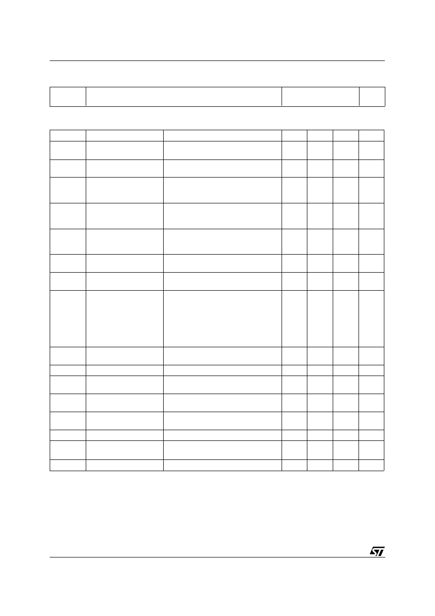
INTERNAL SCHEMATIC DIAGRAM
September 2002
ABSOLUTE MAXIMUM RATINGS
Symbol
Parameter
Value
Unit
V
CBO
Collector-Base Voltage (I
E
= 0)
75
V
V
CER
Collector-Emitter Voltage (R
BE
≤
10
Ω¦
)
50
V
V
EBO
Emitter-Base Voltage (I
C
= 0)
7
V
I
C
Collector Current
500
mA
P
tot
Total Dissipation at T
amb
≤
25
o
C
at T
C
≤
25
o
C
at T
C
≤
100
o
C
0.8
3
1.7
W
W
W
T
stg
Storage Temperature
-65 to 175
o
C
T
j
Max. Operating Junction Temperature
175
o
C
TO-39
1/4
Obsolete Product(s) - Obsolete Product(s)
THERMAL DATA
R
thj-case
R
thj-amb
Thermal Resistance Junction-Case Max
Thermal Resistance Junction-Ambient Max
50
187.5
o
C/W
o
C/W
ELECTRICAL CHARACTERISTICS (T
case
= 25
o
C unless otherwise specified)
Symbol
Parameter
Test Conditions
Min.
Typ.
Max.
Unit
I
CBO
Collector Cut-off
Current (I
E
= 0)
V
CB
= 60 V
V
CB
= 60 V T
C
= 150
o
C
10
10
nA
µ
A
I
EBO
Emitter Cut-off Current
(I
C
= 0)
V
EB
= 5 V
5
nA
V
(BR)CBO
Collector-Base
Breakdown Voltage
(I
E
= 0)
I
C
= 100
µ
A
75
V
V
(BR)CER
Collector-Emitter
Breakdown Voltage
(R
BE
≤
10
Ω¦
)
I
C
= 10 mA
50
V
V
(BR)EBO
Emitter-Base
Breakdown Voltage
(I
C
= 0)
I
E
= 100
µ
A
7
V
V
CE(sat)
Collector-Emitter
Saturation Voltage
I
C
= 150 mA I
B
= 15 mA
0.5
1.5
V
V
BE(sat)
Base-Emitter
Saturation Voltage
I
C
= 150 mA I
B
= 15 mA
0.95
1.3
V
h
FE
DC Current Gain
I
C
= 10
µ
A V
CE
= 10 V
I
C
= 0.1 mA V
CE
= 10 V
I
C
= 10 mA V
CE
= 10 V
I
C
= 150 mA V
CE
= 10 V
I
C
= 500 mA V
CE
= 10 V
I
C
= 10 mA V
CE
= 10 V
T
C
= -55
o
C
20
35
75
100
40
35
60
80
130
130
75
65
300
h
fe
Small Signal Current
Gain
I
C
= 1 mA V
CE
= 10 V f = 1 KHz
70
135
300
f
T
Transition Frequency
I
C
= 50 mA V
CE
= 10 V f = 20 MHz
70
100
MHz
C
EBO
Emitter-Base
Capacitance
I
C
= 0 V
EB
= 0.5 V f = 1 MHz
50
80
pF
C
CBO
Collector-Base
Capacitance
I
E
= 0 V
CB
= 10 V f = 1 MHz
18
25
pF
NF
Noise Figure
I
C
= 0.3 mA V
CE
= 10 V
R
g
= 510
Ω¦
f = 1 KHz
3.5
8
dB
h
ie
Input Impedance
I
C
= 1 mA V
CE
= 5 V f = 1 KHz
4.4
K
Ω¦
h
re
Reverse Voltage Ratio
I
C
= 1 mA V
CE
= 5 V f = 1 KHz
7.3 x
10
-4
h
oe
Output Admittance
I
C
= 1 mA V
CE
= 5 V f = 1 KHz
23.8
µ
S
Pulsed: Pulse duration = 300
µ
s, duty cycle
≤
1 %
2N1711
2/4
Obsolete Product(s) - Obsolete Product(s)
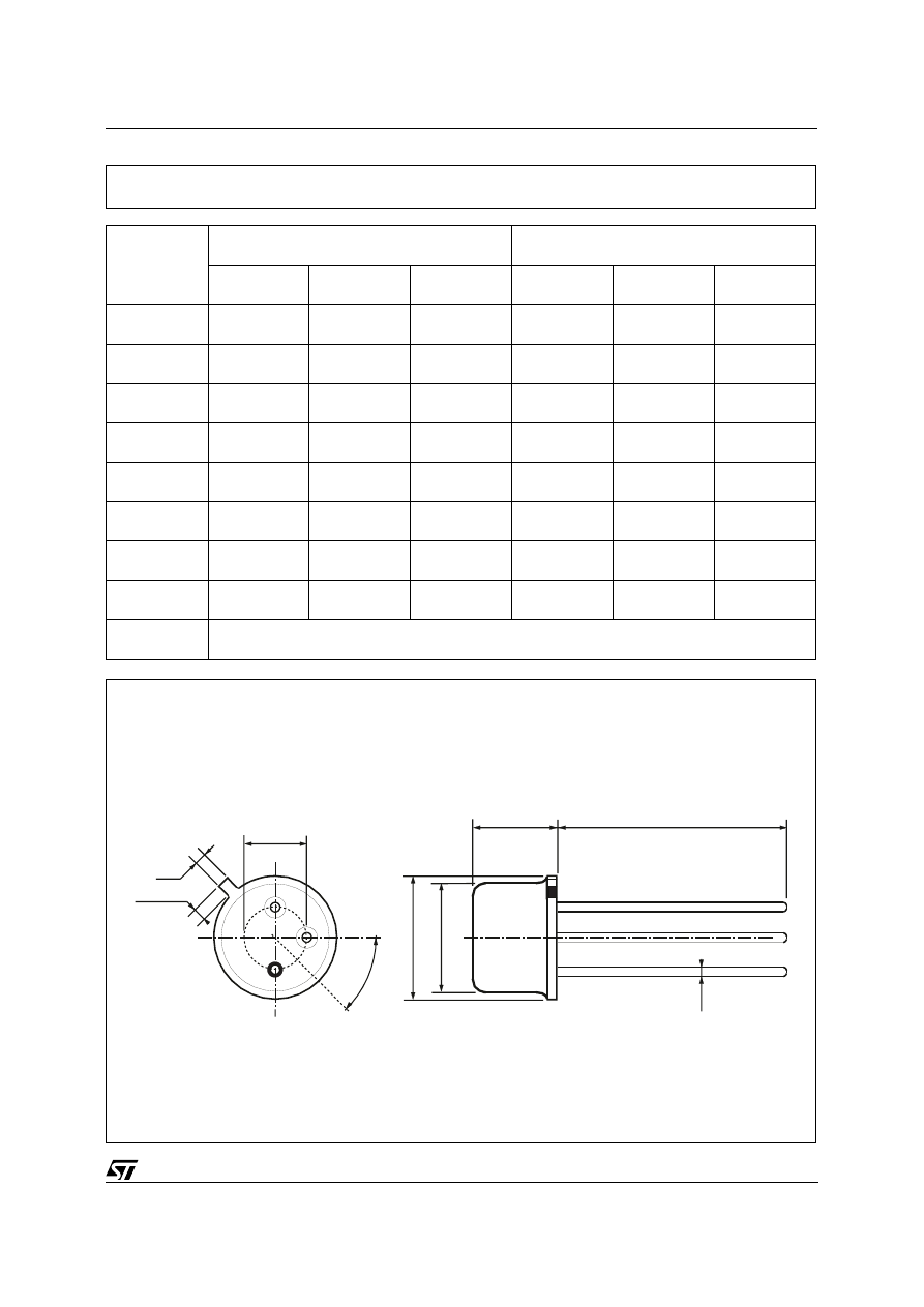
DIM.
mm
inch
MIN.
TYP.
MAX.
MIN.
TYP.
MAX.
A
12.7
0.500
B
0.49
0.019
D
6.6
0.260
E
8.5
0.334
F
9.4
0.370
G
5.08
0.200
H
1.2
0.047
I
0.9
0.035
L
45
o
(typ.)
L
G
I
D
A
F
E
B
H
P008B
TO-39 MECHANICAL DATA
2N1711
3/4
Obsolete Product(s) - Obsolete Product(s)

Information furnished is believed to be accurate and reliable. However, STMicroelectronics assumes no responsibility for the consequences
of use of such information nor for any infringement of patents or other rights of third parties which may result from its use. No license is
granted by implication or otherwise under any patent or patent rights of STMicroelectronics. Specification mentioned in this publication are
subject to change without notice. This publication supersedes and replaces all information previously supplied. STMicroelectronics products
are not authorized for use as critical components in life support devices or systems without express written approval of STMicroelectronics.
The ST logo is a trademark of STMicroelectronics
© 2002 STMicroelectronics - Printed in Italy - All Rights Reserved
STMicroelectronics GROUP OF COMPANIES
Australia - Brazil - Canada - China - Finland - France - Germany - Hong Kong - India - Israel - Italy - Japan - Malaysia - Malta - Morocco -
Singapore - Spain - Sweden - Switzerland - United Kingdom - United States.
http://www.st.com
2N1711
4/4
Obsolete Product(s) - Obsolete Product(s)

