| Secciones |
|---|
| Foros Electrónica |
|
|
| Boletines de correo |
 |
2
N
3906 / MMBT3906 / PZT
3906
P
N
P Gen
e
ra
l-Purpose
Amplifier
© 2010 Fairchild Semiconductor Corporation
www.fairchildsemi.com
2N3906 / MMBT3906 / PZT3906 Rev. 1.2.2
1
April 2014
2N3906 / MMBT3906 / PZT3906
PNP General-Purpose Amplifier
Ordering Information
Part Number
Marking
Package
Packing Method
Pack Quantity
2N3906BU
2N3906
TO-92 3L
Bulk
10000
2N3906TA
2N3906
TO-92 3L
Ammo
2000
2N3906TAR
2N3906
TO-92 3L
Ammo
2000
2N3906TF
2N3906
TO-92 3L
Tape and Reel
2000
2N3906TFR
2N3906
TO-92 3L
Tape and Reel
2000
MMBT3906
2A
SOT-23 3L
Tape and Reel
3000
PZT3906
3906
SOT-223 4L
Tape and Reel
2500
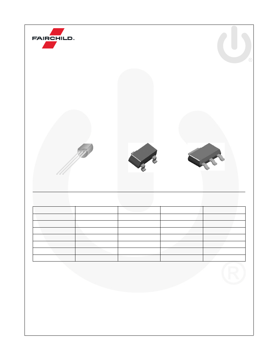
2N3906
MMBT3906
PZT3906
E B C
TO-92
SOT-23
SOT-223
Mark:2A
C
B
E
E
B
C
C
Description
This device is designed for general-purpose amplifier
and switching applications at collector currents of 10 mA
to 100 mA.
2
N
3906 / MMBT3906 / PZT
3906
P
N
P Gen
e
ra
l-Purpose
Amplifier
© 2010 Fairchild Semiconductor Corporation
www.fairchildsemi.com
2N3906 / MMBT3906 / PZT3906 Rev. 1.2.2
2
Absolute Maximum Ratings
(1)
Stresses exceeding the absolute maximum ratings may damage the device. The device may not function or be opera-
ble above the recommended operating conditions and stressing the parts to these levels is not recommended. In addi-
tion, extended exposure to stresses above the recommended operating conditions may affect device reliability. The
absolute maximum ratings are stress ratings only. Values are at T
A
= 25 °C unless otherwise noted.
Note:
1. These ratings are based on a maximum junction temperature of 150
°C.
These are steady-state limits. Fairchild Semiconductor should be consulted on applications involving pulsed
or low-duty cycle operations.
Thermal Characteristics
Values are at T
A
= 25 °C unless otherwise noted.
Notes:
2. Device is mounted on FR-4 PCB 1.6 inch X 1.6 inch X 0.06 inch.
3. PCB size: FR-4, 76 mm x 114 mm x 1.57 mm (3.0 inch x 4.5 inch x 0.062 inch) with minimum land pattern size.
Symbol
Parameter
Value
Unit
V
CEO
Collector-Emitter Voltage
-40
V
V
CBO
Collector-Base Voltage
-40
V
V
EBO
Emitter-Base Voltage
-5.0
V
I
C
Collector Current - Continuous
-200
mA
T
J,
T
STG
Operating and Storage Junction Temperature Range
-55 to +150
°C
Symbol
Parameter
Maximum
Unit
2N3906
(3)
MMBT3906
(2)
PZT3906
(3)
P
D
Total Device Dissipation
625
350
1,000
mW
Derate Above 25
°C
5.0
2.8
8.0
mW/
°C
R
ΘJC
Thermal Resistance, Junction to Case
83.3
°C/W
R
ΘJA
Thermal Resistance, Junction to Ambient
200
357
125
°C/W
2
N
3906 / MMBT3906 / PZT
3906
P
N
P Gen
e
ra
l-Purpose
Amplifier
© 2010 Fairchild Semiconductor Corporation
www.fairchildsemi.com
2N3906 / MMBT3906 / PZT3906 Rev. 1.2.2
3
Electrical Characteristics
Values are at T
A
= 25 °C unless otherwise noted.
Note:
4. Pulse test: pulse width
≤ 300 μs, duty cycle ≤ 2.0%.
Symbol
Parameter
Conditions
Min.
Max.
Unit
OFF CHARACTERISTICS
V
(BR)CEO
Collector-Emitter Breakdown
Voltage
(4)
I
C
= -1.0 mA, I
B
= 0
-40
V
V
(BR)CBO
Collector-Base Breakdown Voltage I
C
= -10
μA, I
E
= 0
-40
V
V
(BR)EBO
Emitter-Base Breakdown Voltage
I
E
= -10
μA, I
C
= 0
-5.0
V
I
BL
Base Cut-Off Current
V
CE
= -30 V, V
BE
= 3.0 V
-50
nA
I
CEX
Collector Cut-Off Current
V
CE
= -30 V, V
BE
= 3.0 V
-50
nA
ON CHARACTERISTICS
h
FE
DC Current Gain
(4)
I
C
= -0.1 mA, V
CE
= -1.0 V
60
I
C
= -1.0 mA, V
CE
= -1.0 V
80
I
C
= -10 mA, V
CE
= -1.0 V
100
300
I
C
= -50 mA, V
CE
= -1.0 V
60
I
C
= -100 mA, V
CE
= -1.0V
30
V
CE
(sat)
Collector-Emitter Saturation
Voltage
I
C
= -10 mA, I
B
= -1.0 mA
-0.25
V
I
C
= -50 mA, I
B
= -5.0 mA
-0.40
V
BE
(sat)
Base-Emitter Saturation Voltage
I
C
= -10 mA, I
B
= -1.0 mA
-0.65
-0.85
V
I
C
= -50 mA, I
B
= -5.0 mA
-0.95
SMALL SIGNAL CHARACTERISTICS
f
T
Current Gain - Bandwidth Product
I
C
= -10 mA, V
CE
= -20 V,
f = 100 MHz
250
MHz
C
obo
Output Capacitance
V
CB
= -5.0 V, I
E
= 0,
f = 100 kHz
4.5
pF
C
ibo
Input Capacitance
V
EB
= -0.5 V, I
C
= 0,
f = 100 kHz
10.0
pF
NF
Noise Figure
I
C
= -100
μA, V
CE
= -5.0 V,
R
S
= 1.0 k
Ω,
f = 10 Hz to 15.7 kHz
4.0
dB
SWITCHING CHARACTERISTICS
t
d
Delay Time
V
CC
= -3.0 V, V
BE
= -0.5 V
I
C
= -10 mA, I
B1
= -1.0 mA
35
ns
t
r
Rise Time
35
ns
t
s
Storage Time
V
CC
= -3.0 V, I
C
= -10 mA,
I
B1
= I
B2
= -1.0 mA
225
ns
t
f
Fall Time
75
ns
2
N
3906 / MMBT3906 / PZT
3906
P
N
P Gen
e
ra
l-Purpose
Amplifier
© 2010 Fairchild Semiconductor Corporation
www.fairchildsemi.com
2N3906 / MMBT3906 / PZT3906 Rev. 1.2.2
4
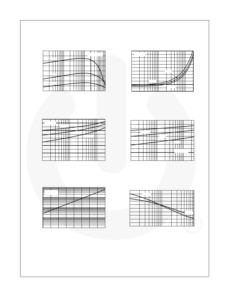
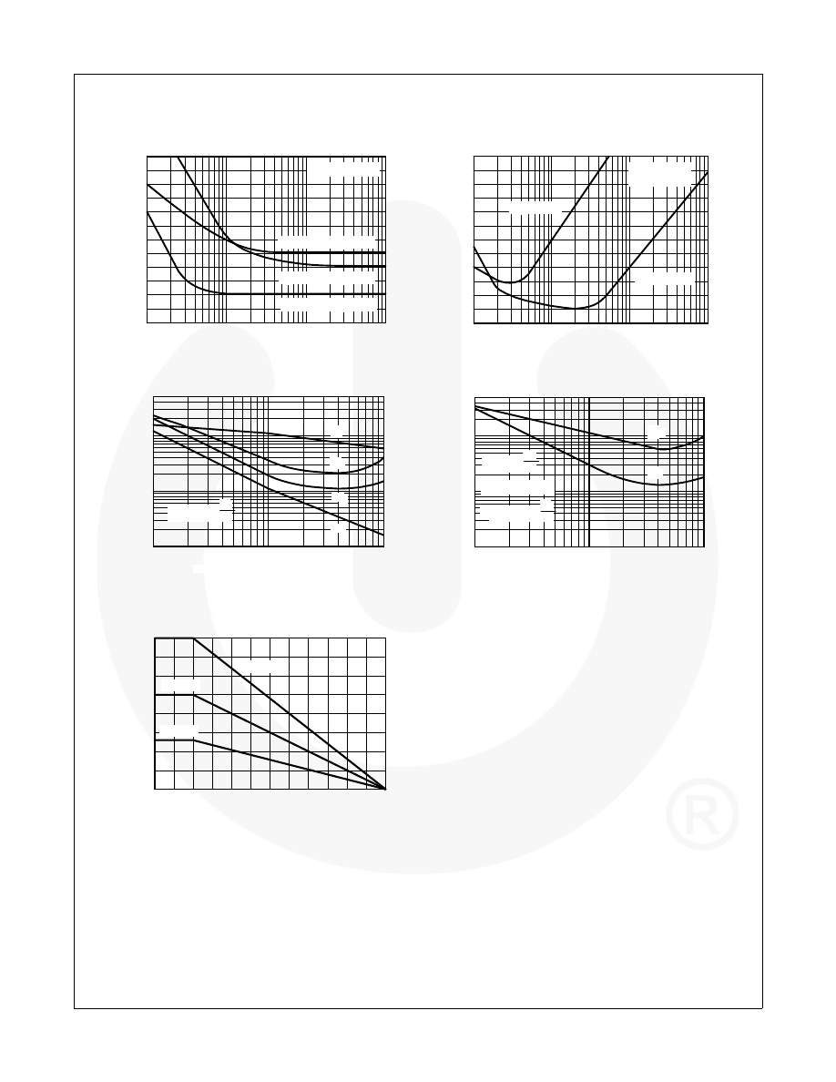
Typical Performance Characteristics
Figure 1. Typical Pulsed Current Gain vs. Collector
Current
Figure 2. Collector-Emitter Saturation Voltage vs.
Collector Current
Figure 3. Base-Emitter Saturation Voltage
vs. Collector Current
Figure 4. Base-Emitter On Voltage vs.
Collector Current
Figure 5. Collector Cut-Off Current vs.
Ambient Temperature
Figure 6. Common-Base Open Circuit Input and Out-
put Capacitance vs. Reverse Bias Voltage
0.1 0.2
0.5
1
2
5
10
20
50 100
50
100
150
200
250
I - COLLECTOR CURRE NT (mA)
h
-
T
YPI
C
A
L
P
U
L
SED
C
U
R
R
EN
T
G
A
IN
C
FE
125 °C
25 °C
- 40 °C
V = 1.0V
CE
1
10
100
200
0
0.05
0.1
0.15
0.2
0.25
0.3
I - COLLECTOR CURRENT (mA)
V
-
C
O
L
L
E
C
T
O
R
E
M
IT
T
E
R
V
O
L
TA
G
E
(
V
)
C
CE
S
A
T
25 °C
- 40 °C
125 °C
β = 10
1
10
100
200
0
0.2
0.4
0.6
0.8
1
I - COLLECTOR CURRE NT (mA)
V
-
B
A
S
E
E
M
IT
T
E
R
V
O
L
TA
G
E
(
V
)
C
BE
S
A
T
β = 10
25 °C
- 40 °C
125 °C
0.1
1
10
25
0
0.2
0.4
0.6
0.8
1
I - COLLECTOR CURRENT (mA)
V
-
B
A
S
E
E
M
IT
T
E
R
O
N
V
O
L
TA
G
E
(
V
)
C
BE
(O
N
)
V = 1V
CE
25 °C
- 40 °C
125 °C
25
50
75
100
125
0.01
0.1
1
10
100
T - AMBIE NT TEMP ERATURE ( C)
I
- C
O
L
LE
C
T
O
R
CU
RR
E
N
T
(
n
A)
A
CBO
°
V = 25V
CB
0.1
1
10
0
2
4
6
8
10
REVERSE BIAS VOLTAGE (V)
CA
P
A
CI
TA
NCE (
p
F
)
C obo
C ibo
2
N
3906 / MMBT3906 / PZT
3906
P
N
P Gen
e
ra
l-Purpose
Amplifier
© 2010 Fairchild Semiconductor Corporation
www.fairchildsemi.com
2N3906 / MMBT3906 / PZT3906 Rev. 1.2.2
5
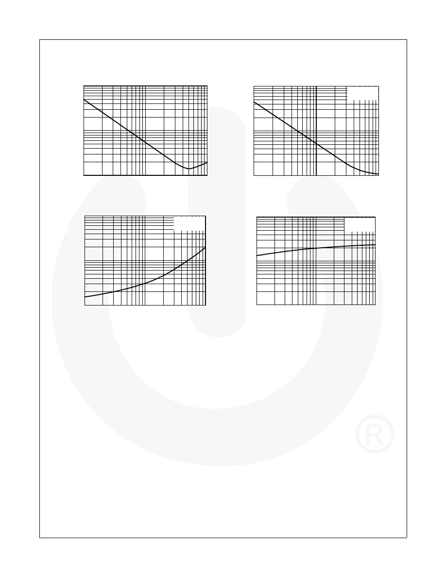
Typical Performance Characteristics
(Continued)
Figure 7. Noise Figure vs. Frequency
Figure 8. Noise Figure vs. Source Resistance
Figure 9. Switching Times vs. Collector Current
Figure 10. Turn-On and Turn-Off Times vs.
Collector Current
Figure 11. Power Dissipation vs.
Ambient Temperature
0.1
1
10
100
0
1
2
3
4
5
6
f - FREQUENCY (kHz)
NF
-
NO
IS
E
F
IG
U
R
E
(
d
B)
I = 100 μA, R = 200Ω
C
V = 5.0V
CE
S
I = 100 μA, R = 2.0 kΩ
C
S
I = 1.0 mA, R = 200Ω
C
S
0.1
1
10
100
0
2
4
6
8
10
12
R - SOURCE RESISTANCE ( )
NF
-
NO
IS
E
F
IG
U
RE
(
d
B)
k
Ω
I = 100
μA
C
V = 5.0V
f = 1.0 kHz
CE
I = 1.0 mA
C
S
1
10
100
1
10
100
500
I - COLLECTOR CURRENT (mA)
T
IME
(n
S
)
I = I =
t r
t
s
B1
C
B2
I
c
10
t f
t d
1
10
100
1
10
100
500
I - COLLECTOR CURRENT (mA)
TI
M
E
(n
S
)
I = I =
t
off
B1
B2
I
c
10
t
on
V = 0.5V
BE(OFF)
t
I =
on
t
off
B1
I
c
10
0
25
50
75
100
125
150
0
0.25
0.5
0.75
1
TEMPERATURE ( C)
P
-
PO
W
E
R
D
ISSI
P
A
TI
O
N
(
W
)
D
o
SOT-223
SOT-23
TO-92
2
N
3906 / MMBT3906 / PZT
3906
P
N
P Gen
e
ra
l-Purpose
Amplifier
© 2010 Fairchild Semiconductor Corporation
www.fairchildsemi.com
2N3906 / MMBT3906 / PZT3906 Rev. 1.2.2
6
Typical Performance Characteristics
(Continued)
Figure 12. Voltage Feedback Ratio
Figure 13. Input Impedance
Figure 14. Output Admittance
Figure 15. Current Gain
0.1
1
10
1
10
100
I - COLLECTOR CURRENT (mA)
h
-
V
O
LT
A
G
E
F
E
E
D
B
A
C
K
R
A
T
IO
(
x1
0
)
C
re
_
4
0.1
1
10
0.1
1
10
I - COLLECTOR CURRENT (mA)
h
-
I
N
PU
T I
M
PED
ANC
E
(k
)
V = 10 V
CE
C
ie
f = 1.0 kHz
Ω
0.1
1
10
10
100
1000
I - COLLECTOR CURRENT (mA)
h
-
O
U
TPU
T
A
D
M
IT
T
A
N
C
E
(
m
h
os
)
V = 10 V
CE
C
oe
f = 1.0 kHz
μ
0.1
1
10
10
20
50
100
200
500
1000
I - COLLECTOR CURRENT (mA)
h
- C
U
R
R
E
N
T G
A
IN
V = 10 V
CE
C
fe
f = 1.0 kHz

2
N
3906 / MMBT3906 / PZT
3906
P
N
P Gen
e
ra
l-Purpose
Amplifier
© 2010 Fairchild Semiconductor Corporation
www.fairchildsemi.com
2N3906 / MMBT3906 / PZT3906 Rev. 1.2.2
7
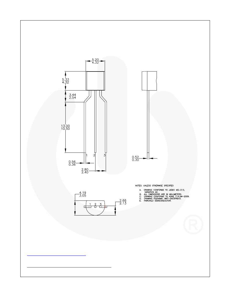
Physical Dimensions
Figure 16. 3-LEAD, TO92, JEDEC TO-92 COMPLIANT STRAIGHT LEAD CONFIGURATION (OLD TO92AM3)
Package drawings are provided as a service to customers considering Fairchild components. Drawings may change in any manner
without notice. Please note the revision and/or date on the drawing and contact a Fairchild Semiconductor representative to verify or
obtain the most recent revision. Package specifications do not expand the terms of Fairchilds worldwide terms and conditions, specifically the
warranty therein, which covers Fairchild products.
Always visit Fairchild Semiconductors online packaging area for the most recent package drawings:
http://www.fairchildsemi.com/dwg/ZA/ZA03D.pdf
.
For current tape and reel specifications, visit Fairchild Semiconductors online packaging area:
http://www.fairchildsemi.com/packing_dwg/PKG-ZA03D_BK.pdf
.
D
TO-92 (Bulk)
2
N
3906 / MMBT3906 / PZT
3906
P
N
P Gen
e
ra
l-Purpose
Amplifier
© 2010 Fairchild Semiconductor Corporation
www.fairchildsemi.com
2N3906 / MMBT3906 / PZT3906 Rev. 1.2.2
8
Physical Dimensions
(Continued)
Figure 17. 3-LEAD, TO92, MOLDED 0.200 IN LINE SPACING LEAD FORM (J61Z OPTION)
Package drawings are provided as a service to customers considering Fairchild components. Drawings may change in any manner
without notice. Please note the revision and/or date on the drawing and contact a Fairchild Semiconductor representative to verify or
obtain the most recent revision. Package specifications do not expand the terms of Fairchilds worldwide terms and conditions, specifically the
warranty therein, which covers Fairchild products.
Always visit Fairchild Semiconductors online packaging area for the most recent package drawings:
http://www.fairchildsemi.com/dwg/ZA/ZA03F.pdf
.
For current tape and reel specifications, visit Fairchild Semiconductors online packaging area:
http://www.fairchildsemi.com/packing_dwg/PKG-ZA03F_BK.pdf
.
TO-92 (Ammo, Tape and Reel)
2
N
3906 / MMBT3906 / PZT
3906
P
N
P Gen
e
ra
l-Purpose
Amplifier
© 2010 Fairchild Semiconductor Corporation
www.fairchildsemi.com
2N3906 / MMBT3906 / PZT3906 Rev. 1.2.2
9
Physical Dimensions
(Continued)
Figure 18. 3-LEAD, SOT23, JEDEC TO-236, LOW PROFILE
Package drawings are provided as a service to customers considering Fairchild components. Drawings may change in any manner
without notice. Please note the revision and/or date on the drawing and contact a Fairchild Semiconductor representative to verify or
obtain the most recent revision. Package specifications do not expand the terms of Fairchilds worldwide terms and conditions, specifically the
warranty therein, which covers Fairchild products.
Always visit Fairchild Semiconductors online packaging area for the most recent package drawings:
http://www.fairchildsemi.com/dwg/MA/MA03D.pdf
.
For current tape and reel specifications, visit Fairchild Semiconductors online packaging area:
http://www.fairchildsemi.com/packing_dwg/PKG-MA03D.pdf
.
LAND PATTERN
RECOMMENDATION
NOTES: UNLESS OTHERWISE SPECIFIED
A) REFERENCE JEDEC REGISTRATION
TO-236, VARIATION AB, ISSUE H.
B) ALL DIMENSIONS ARE IN MILLIMETERS.
C) DIMENSIONS ARE INCLUSIVE OF BURRS,
MOLD FLASH AND TIE BAR EXTRUSIONS.
D) DIMENSIONING AND TOLERANCING PER
ASME Y14.5M - 1994.
E) DRAWING FILE NAME: MA03DREV10
3
1
2
SEE DETAIL A
SEATING
PLANE
SCALE: 2X
GAGE PLANE
(0.55)
(0.93)
1.20 MAX
C
0.10
0.00
0.10
C
2.40 ±0.30
2.92 ±0.20
1.30+0.20
-0.15
0.60
0.37
0.20
A B
1.90
0.95
(0.29)
0.95
1.40
2.20
1.00
1.90
0.25
0.23
0.08
0.20 MIN
SOT-23
2
N
3906 / MMBT3906 / PZT
3906
P
N
P Gen
e
ra
l-Purpose
Amplifier
© 2010 Fairchild Semiconductor Corporation
www.fairchildsemi.com
2N3906 / MMBT3906 / PZT3906 Rev. 1.2.2
10
Physical Dimensions
(Continued)
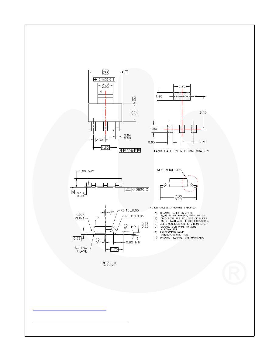
Figure 19. MOLDED PACKAGE, SOT-223, 4-LEAD
Package drawings are provided as a service to customers considering Fairchild components. Drawings may change in any manner
without notice. Please note the revision and/or date on the drawing and contact a Fairchild Semiconductor representative to verify or
obtain the most recent revision. Package specifications do not expand the terms of Fairchilds worldwide terms and conditions, specifically the
warranty therein, which covers Fairchild products.
Always visit Fairchild Semiconductors online packaging area for the most recent package drawings:
http://www.fairchildsemi.com/dwg/MA/MA04A.pdf
.
For current tape and reel specifications, visit Fairchild Semiconductors online packaging area:
http://www.fairchildsemi.com/packing_dwg/PKG-MA04A_BK.pdf
.
SOT-223 4L
© Fairchild Semiconductor Corporation
www.fairchildsemi.com
TRADEMARKS
The following includes registered and unregistered trademarks and service marks, owned by Fairchild Semiconductor and/or its global subsidiaries, and is not
intended to be an exhaustive list of all such trademarks.
AccuPower ¥
AX-CAP
®
*
BitSiC ¥
Build it Now ¥
CorePLUS ¥
CorePOWER ¥
CROSSVOLT ¥
CTL ¥
Current Transfer Logic ¥
DEUXPEED
®
Dual Cool™
EcoSPARK
®
EfficientMax ¥
ESBC ¥
Fairchild
®
Fairchild Semiconductor
®
FACT Quiet Series ¥
FACT
®
FAST
®
FastvCore ¥
FETBench ¥
FPS ¥
F-PFS ¥
FRFET
®
Global Power Resource
SM
GreenBridge ¥
Green FPS ¥
Green FPS ¥ e-Series ¥
Gmax ¥
GTO ¥
IntelliMAX ¥
ISOPLANAR ¥
Making Small Speakers Sound Louder
and Better™
MegaBuck ¥
MICROCOUPLER ¥
MicroFET ¥
MicroPak ¥
MicroPak2 ¥
MillerDrive ¥
MotionMax ¥
mWSaver
®
OptoHiT ¥
OPTOLOGIC
®
OPTOPLANAR
®
®
PowerTrench
®
PowerXS™
Programmable Active Droop ¥
QFET
®
QS ¥
Quiet Series ¥
RapidConfigure ¥
¥
Saving our world, 1mW/W/kW at a time™
SignalWise ¥
SmartMax ¥
SMART START ¥
Solutions for Your Success ¥
SPM
®
STEALTH ¥
SuperFET
®
SuperSOT ¥-3
SuperSOT ¥-6
SuperSOT ¥-8
SupreMOS
®
SyncFET ¥
Sync-Lock™
®*
TinyBoost
®
TinyBuck
®
TinyCalc ¥
TinyLogic
®
TINYOPTO ¥
TinyPower ¥
TinyPWM ¥
TinyWire ¥
TranSiC ¥
TriFault Detect ¥
TRUECURRENT
®
*
PSerDes ¥
UHC
®
Ultra FRFET ¥
UniFET ¥
VCX ¥
VisualMax ¥
VoltagePlus ¥
XS™
௺
™
* Trademarks of System General Corporation, used under license by Fairchild Semiconductor.
DISCLAIMER
FAIRCHILD SEMICONDUCTOR RESERVES THE RIGHT TO MAKE CHANGES WITHOUT FURTHER NOTICE TO ANY PRODUCTS HEREIN TO IMPROVE
RELIABILITY, FUNCTION, OR DESIGN. FAIRCHILD DOES NOT ASSUME ANY LIABILITY ARISING OUT OF THE APPLICATION OR USE OF ANY PRODUCT
OR CIRCUIT DESCRIBED HEREIN; NEITHER DOES IT CONVEY ANY LICENSE UNDER ITS PATENT RIGHTS, NOR THE RIGHTS OF OTHERS. THESE
SPECIFICATIONS DO NOT EXPAND THE TERMS OF FAIRCHILDS WORLDWIDE TERMS AND CONDITIONS, SPECIFICALLY THE WARRANTY THEREIN,
WHICH COVERS THESE PRODUCTS.
LIFE SUPPORT POLICY
FAIRCHILDS PRODUCTS ARE NOT AUTHORIZED FOR USE AS CRITICAL COMPONENTS IN LIFE SUPPORT DEVICES OR SYSTEMS WITHOUT THE
EXPRESS WRITTEN APPROVAL OF FAIRCHILD SEMICONDUCTOR CORPORATION.
As used herein:
1. Life support devices or systems are devices or systems which, (a) are
intended for surgical implant into the body or (b) support or sustain
life, and (c) whose failure to perform when properly used in
accordance with instructions for use provided in the labeling, can be
reasonably expected to result in a significant injury of the user.
2. A critical component in any component of a life support, device, or
system whose failure to perform can be reasonably expected to
cause the failure of the life support device or system, or to affect its
safety or effectiveness.
ANTI-COUNTERFEITING POLICY
Fairchild Semiconductor Corporation's Anti-Counterfeiting Policy. Fairchild's Anti-Counterfeiting Policy is also stated on our external website, www.fairchildsemi.com,
under Sales Support.
Counterfeiting of semiconductor parts is a growing problem in the industry. All manufacturers of semiconductor products are experiencing counterfeiting of their
parts. Customers who inadvertently purchase counterfeit parts experience many problems such as loss of brand reputation, substandard performance, failed
applications, and increased cost of production and manufacturing delays. Fairchild is taking strong measures to protect ourselves and our customers from the
proliferation of counterfeit parts. Fairchild strongly encourages customers to purchase Fairchild parts either directly from Fairchild or from Authorized Fairchild
Distributors who are listed by country on our web page cited above. Products customers buy either from Fairchild directly or from Authorized Fairchild Distributors
are genuine parts, have full traceability, meet Fairchild's quality standards for handling and storage and provide access to Fairchild's full range of up-to-date technical
and product information. Fairchild and our Authorized Distributors will stand behind all warranties and will appropriately address any warranty issues that may arise.
Fairchild will not provide any warranty coverage or other assistance for parts bought from Unauthorized Sources. Fairchild is committed to combat this global
problem and encourage our customers to do their part in stopping this practice by buying direct or from authorized distributors.
PRODUCT STATUS DEFINITIONS
Definition of Terms
Datasheet Identification
Product Status
Definition
Advance Information
Formative / In Design Datasheet contains the design specifications for product development. Specifications may change
in any manner without notice.
Preliminary First
Production
Datasheet contains preliminary data; supplementary data will be published at a later date. Fairchild
Semiconductor reserves the right to make changes at any time without notice to improve design.
No Identification Needed
Full Production
Datasheet contains final specifications. Fairchild Semiconductor reserves the right to make
changes at any time without notice to improve the design.
Obsolete
Not In Production
Datasheet contains specifications on a product that is discontinued by Fairchild Semiconductor.
The datasheet is for reference information only.
Rev. I68
®

