| Secciones |
|---|
| Foros Electrónica |
|
|
| Boletines de correo |
 |

Atmel-8735C-SEEPROM-AT93C56B-66B-Datasheet_012015
Features
ï¬
Low-voltage Operation
̶
V
CC
= 1.7V to 5.5V
ï¬
User-selectable Internal Organization
̶
2K: 256 x 8 or 128 x 16
̶
4K: 512 x 8 or 256 x 16
ï¬
3-wire Serial Interface
ï¬
Sequential Read Operation
ï¬
2MHz Clock Rate (5V)
ï¬
Self-timed Write Cycle (5ms Max)
ï¬
High Reliability
̶
Endurance: 1,000,000 Write Cycles
̶
Data Retention: 100 Years
ï¬
8-lead JEDEC SOIC, 8-lead TSSOP, 8-pad UDFN, 8-pad XDFN, and
8-ball VFBGA packages
Description
The Atmel
®
AT93C56B/66B provides 2,048/4,096 bits of Serial Electrically
Erasable Programmable Read-Only Memory (EEPROM) organized as 128/256
words of 16 bits each (when the ORG pin is connected to V
CC
) and 256/512 words
of 8 bits each (when the ORG pin is tied to ground). The device is optimized for
use in many industrial and commercial applications where low-power and low-
voltage operations are essential. The AT93C56B/66B is available in space-saving
8-lead JEDEC SOIC, 8-lead TSSOP, 8-pad UDFN, 8-pad XDFN, and 8-ball
VFBGA packages.
The AT93C56B/66B is enabled through the Chip Select pin (CS) and accessed
via a 3-wire serial interface consisting of Data Input (DI), Data Output (DO), and
Shift Clock (SK). Upon receiving a Read instruction at DI, the address is decoded,
and the data is clocked out serially on the DO pin. The write cycle is completely
self-timed, and no separate erase cycle is required before Write. The write cycle is
only enabled when the part is in the Erase/Write Enable state. When CS is
brought high following the initiation of a write cycle, the DO pin outputs the
Ready/Busy status of the part.
The AT93C56B/66B operates from 1.7V to 5.5V.
AT93C56B and AT93C66B
3-wire Serial EEPROM
2K (256 x 8 or 128 x 16) and 4K (512 x 8 or 256 x 16)
DATASHEET
AT93C56B/66B [DATASHEET]
Atmel-8735C-SEEPROM-AT93C56B-66B-Datasheet_012015
2
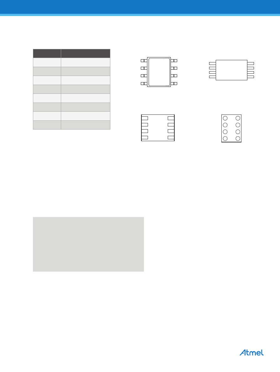
1.
Pin Configurations and Pinouts
Table 1-1.
Pin Configurations
2.
Absolute Maximum Ratings*
Pin Name
Function
CS
Chip Select
SK
Serial Data Clock
DI
Serial Data Input
DO
Serial Data Output
GND
Ground
V
CC
Power Supply
ORG
Internal Organization
NC
No Connect
V
CC
NC
ORG
GND
CS
SK
DI
DO
1
2
3
4
8
7
6
5
8-ball VFBGA
Bottom View
Note: Drawings are not to scale.
8-pad UDFN/XDFN
Bottom View
V
CC
NC
ORG
GND
CS
SK
DI
DO
1
2
3
4
8
7
6
5
Top View
8-lead TSSOP
1
2
3
4
8
7
6
5
CS
SK
DI
DO
V
CC
NC
ORG
GND
Top View
8-lead SOIC
CS
SK
DI
DO
V
CC
NC
ORG
GND
1
2
3
4
8
7
6
5
Operating Temperature
ï ï®ï ï®ï ï®ï ï®ï ï®ï ï®ï ï®ï ï®ï ï®ï ï®ï ï®ï ï55ï°C to +125ï°C
Storage Temperature
ï ï®ï ï®ï ï®ï ï®ï ï®ï ï®ï ï®ï ï®ï ï®ï ï®ï ï®ï ï®ï ï®ï ï65ï°C to +150ï°C
Voltage on any pin
with respect to ground
ï ï®ï ï®ï ï®ï ï®ï ï®ï ï®ï ï®ï ï®ï ï®ï ï®ï ï®ï ï®ï ï®ï ï®ï ï1.0V to +7.0V
Maximum Operating Voltage . . . . . . . . . . . . . . . 6.25V
DC Output Current . . . . . . . . . . . . . . . . . . . . . . .5.0mA
*Notice: Stresses beyond those listed under Absolute
Maximum Ratings may cause permanent damage
to the device. This is a stress rating only, and
functional operation of the device at these or any
other conditions beyond those indicated in the
operational sections of this specification is not
implied. Exposure to absolute maximum rating
conditions for extended periods may affect device
reliability.
3
AT93C56B/66B [DATASHEET]
Atmel-8735C-SEEPROM-AT93C56B-66B-Datasheet_012015
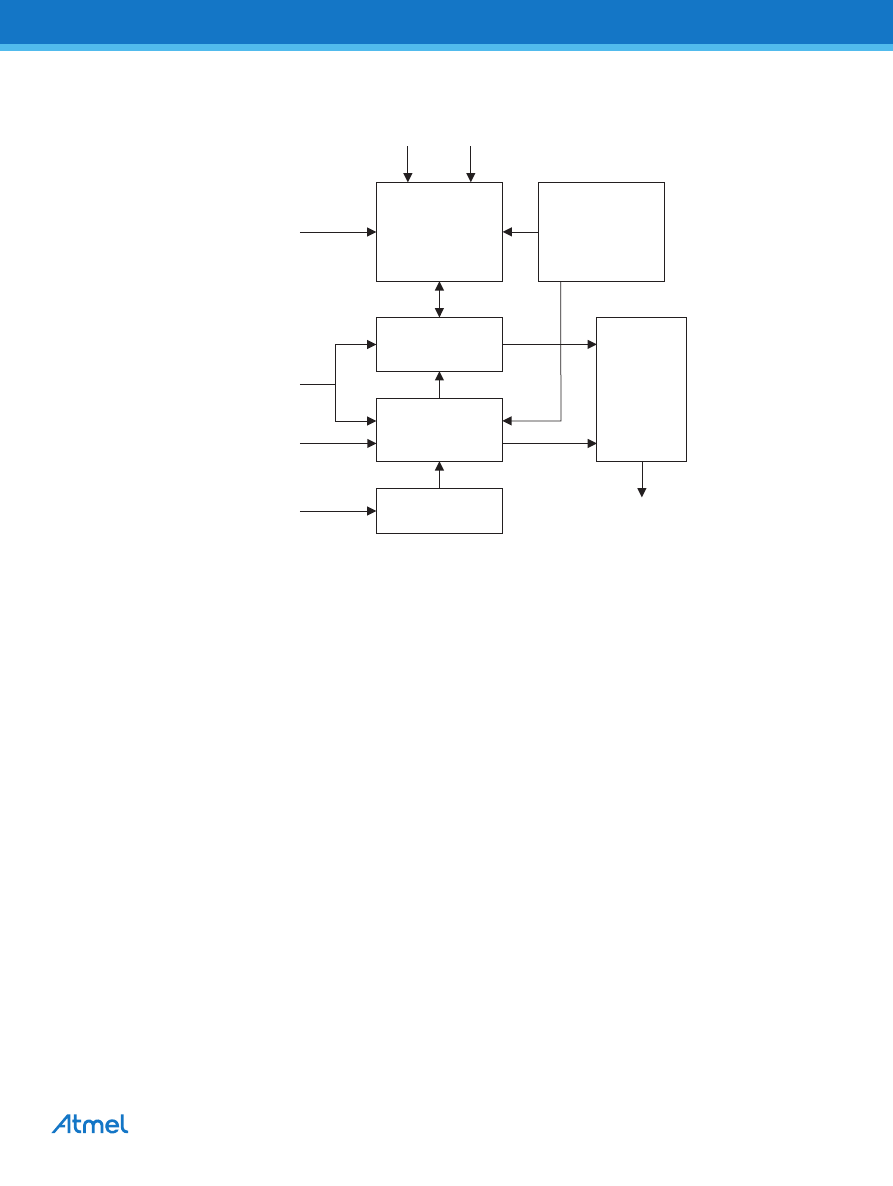
3.
Block Diagram
Note:
When the ORG pin is connected to V
CC
, the x16 organization is selected. When it is connected to ground,
the x8 organization is selected. If the ORG pin is left unconnected, and the application does not load the input
beyond the capability of the internal 1M
Ω
pull-up resistor, then the x16 organization is selected.
ORG
DI
CS
SK
V
CC
GND
Address
Decoder
Output
Buffer
Data
Register
Mode Decode
Logic
Clock
Generator
DO
Memory Array
256/512 x 8
or
128/256 x 16
AT93C56B/66B [DATASHEET]
Atmel-8735C-SEEPROM-AT93C56B-66B-Datasheet_012015
4
4.
Memory Organization
4.1
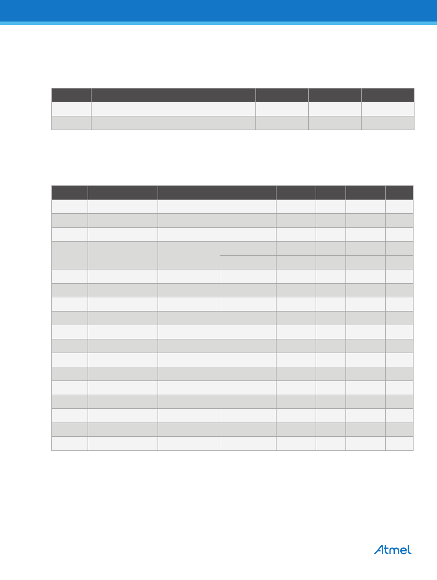
Pin Capacitance
Note:
1.
This parameter is characterized, and is not 100% tested.
4.2
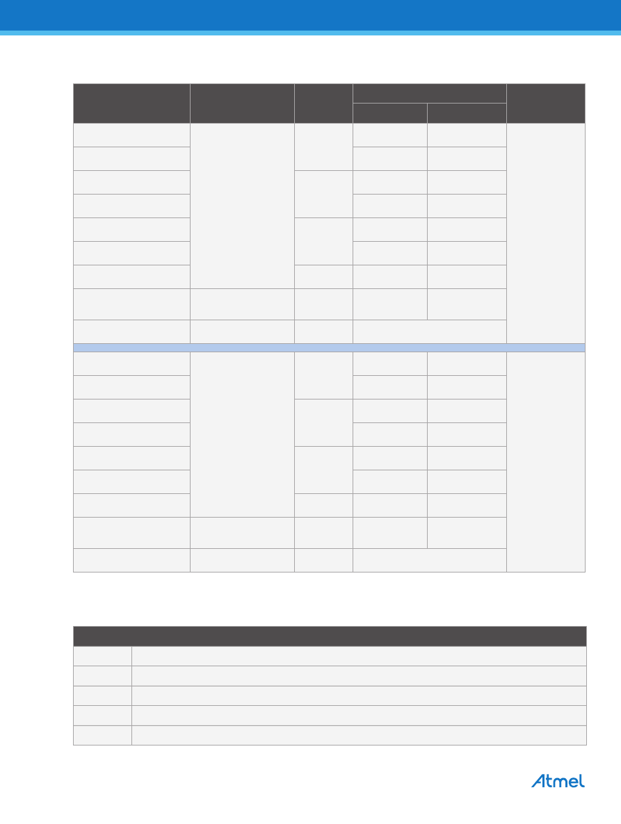
DC Characteristics
Note:
1.
V
IL
min and V
IH
max are reference only, and are not tested.
Applicable over recommended operating range from T
A
= 25
ï°C, f = 1.0MHz, V
CC
= 5.0V (unless otherwise noted).
Symbol
Test Conditions
Max
Units
Conditions
C
OUT
Output Capacitance (DO)
5
pF
V
OUT
= 0V
C
IN
Input Capacitance (CS, SK, DI)
5
pF
V
IN
= 0V
Applicable over recommended operating range from T
AI
= -40 °C to +85 °C, V
CC
= 1.7V to 5.5V (unless otherwise noted).
Symbol
Parameter
Test Condition
Min
Typ
Max
Unit
V
CC1
Supply Voltage
1.7
5.5
V
V
CC2
Supply Voltage
2.5
5.5
V
V
CC3
Supply Voltage
4.5
5.5
V
I
CC
Supply Current
V
CC
= 5.0V
Read at 1.0MHz
0.5
2.0
mA
Write at 1.0MHz
0.5
2.0
mA
I
SB1
Standby Current
V
CC
= 1.7V
CS = 0V
0.4
1.0
μA
I
SB2
Standby Current
V
CC
= 2.5V
CS = 0V
6.0
10.0
μA
I
SB3
Standby Current
V
CC
= 5.0V
CS = 0V
10.0
15.0
μA
I
IL
Input Leakage
V
IN
= 0V to V
CC
0.1
3.0
μA
I
OL
Output Leakage
V
IN
= 0V to V
CC
0.1
3.0
μA
V
IL1
Input Low Voltage
2.5V
ï£ï V
CC
ï£ 5.5V
ï0.6
0.8
V
V
IH1
Input High Voltage
2.5V
ï£ï V
CC
ï£ 5.5V
2.0
V
CC
+ 1
V
V
IL2
Input Low Voltage
1.7V
ï£ V
CC
ï£ 2.5V
ï0.6
V
CC
x 0.3
V
V
IH2
Input High Voltage
1.7V
ï£ V
CC
ï£ 2.5V
V
CC
x 0.7
V
CC
+ 1
V
V
OL1
Output Low Voltage
2.5V
ï£ V
CC
ï£ 5.5V
I
OL
= 2.1mA
0.4
V
V
OH1
Output High Voltage
2.5V
ï£ V
CC
ï£ 5.5V
I
OH
=
ï0.4mA
2.4
V
V
OL2
Output Low Voltage
1.7V
ï£ V
CC
ï£ 2.5V
I
OL
= 0.15mA
0.2
V
V
OH2
Output High Voltage
1.7V
ï£ V
CC
ï£ 2.5V
I
OH
=
ï100μA
V
CC
ï 0.2
V
5
AT93C56B/66B [DATASHEET]
Atmel-8735C-SEEPROM-AT93C56B-66B-Datasheet_012015
4.3
AC Characteristics
Note:
1.
This parameter is characterized, and is not 100% tested.
Applicable over recommended operating range from T
AI
= -40 °C to + 85 °C, V
CC
= as specified, CL = 1 TTL gate and 100pF
(unless otherwise noted).
Symbol
Parameter
Test Condition
Min
Max
Units
f
SK
SK Clock Frequency
4.5V
ï£ V
CC
ï ï£ 5.5V
0
2
MHz
2.5V
ï£ V
CC
ï ï£ 5.5V
0
1
MHz
1.7V
ï£ V
CC
ï ï£ 5.5V
0
250
kHz
t
SKH
SK High Time
2.5V
ï£ V
CC
ï ï£ 5.5V
250
ns
1.7V
ï£ V
CC
ï ï£ 5.5V
1000
ns
t
SKL
SK Low Time
2.5V
ï£ V
CC
ï ï£ 5.5V
250
ns
1.7V
ï£ V
CC
ï ï£ 5.5V
1000
ns
t
CS
Minimum CS Low Time
2.5V
ï£ V
CC
ï ï£ 5.5V
250
ns
1.7V
ï£ V
CC
ï ï£ 5.5V
1000
ns
t
CSS
CS Setup Time
Relative to SK
2.5V
ï£ V
CC
ï ï£ 5.5V
50
ns
1.7V
ï£ V
CC
ï ï£ 5.5V
200
ns
t
DIS
DI Setup Time
Relative to SK
2.5V
ï£ V
CC
ï ï£ 5.5V
100
ns
1.7V
ï£ V
CC
ï ï£ 5.5V
400
ns
t
CSH
CS Hold Time
Relative to SK
0
ns
t
DIH
DI Hold Time
Relative to SK
2.5V
ï£ V
CC
ï ï£ 5.5V
100
ns
1.7V
ï£ V
CC
ï ï£ 5.5V
400
ns
t
PD1
Output Delay to 1
AC Test
2.5V
ï£ V
CC
ï ï£ 5.5V
250
ns
1.7V
ï£ V
CC
ï ï£ 5.5V
1000
ns
t
PD0
Output Delay to 0
AC Test
2.5V
ï£ V
CC
ï ï£ 5.5V
250
ns
1.7V
ï£ V
CC
ï ï£ 5.5V
1000
ns
t
SV
CS to Status Valid
AC Test
2.5V
ï£ V
CC
ï ï£ 5.5V
250
ns
1.7V
ï£ V
CC
ï ï£ 5.5V
1000
ns
t
DF
CS to DO in
High-impedance
AC Test
2.5V
ï£ V
CC
ï ï£ 5.5V
150
ns
CS = V
IL
1.7V
ï£ V
CC
ï ï£ 5.5V
400
ns
t
WP
Write Cycle Time
1.7V
ï£ V
CC
ï ï£ 5.5V
5
ms
Endurance
5.0V, 25 °C
1,000,000
Write Cycles
AT93C56B/66B [DATASHEET]
Atmel-8735C-SEEPROM-AT93C56B-66B-Datasheet_012015
6
5.
Functional Description
The AT93C56B/66B is accessed via a simple and versatile 3-wire serial communication interface. Device
operation is controlled by seven instructions issued by the Host processor. A valid instruction starts with a rising
edge of CS and consists of a Start bit (Logic 1), followed by the appropriate opcode, and the desired memory
address location.
Table 5-1.
AT93C56B/66B Instruction Set
Note:
1.
The Xs in the address field represent dont care values, and must be clocked.
READ: The READ instruction contains the address code for the memory location to be read. After the
instruction and address are decoded, data from the selected memory location is available at the Serial Output
pin, DO. Output data changes are synchronized with the rising edges of the Serial Clock pin, SK. It should be
noted that a dummy bit (Logic 0) precedes the 8-bit or 16-bit data output string. The AT93C56B/66B supports
sequential Read operations. The device will automatically increment the internal address pointer and clock out
the next memory location as long as Chip Select (CS) is held high. In this case, the dummy bit (Logic 0) will not
be clocked out between memory locations, thus allowing for a continuous stream of data to be read.
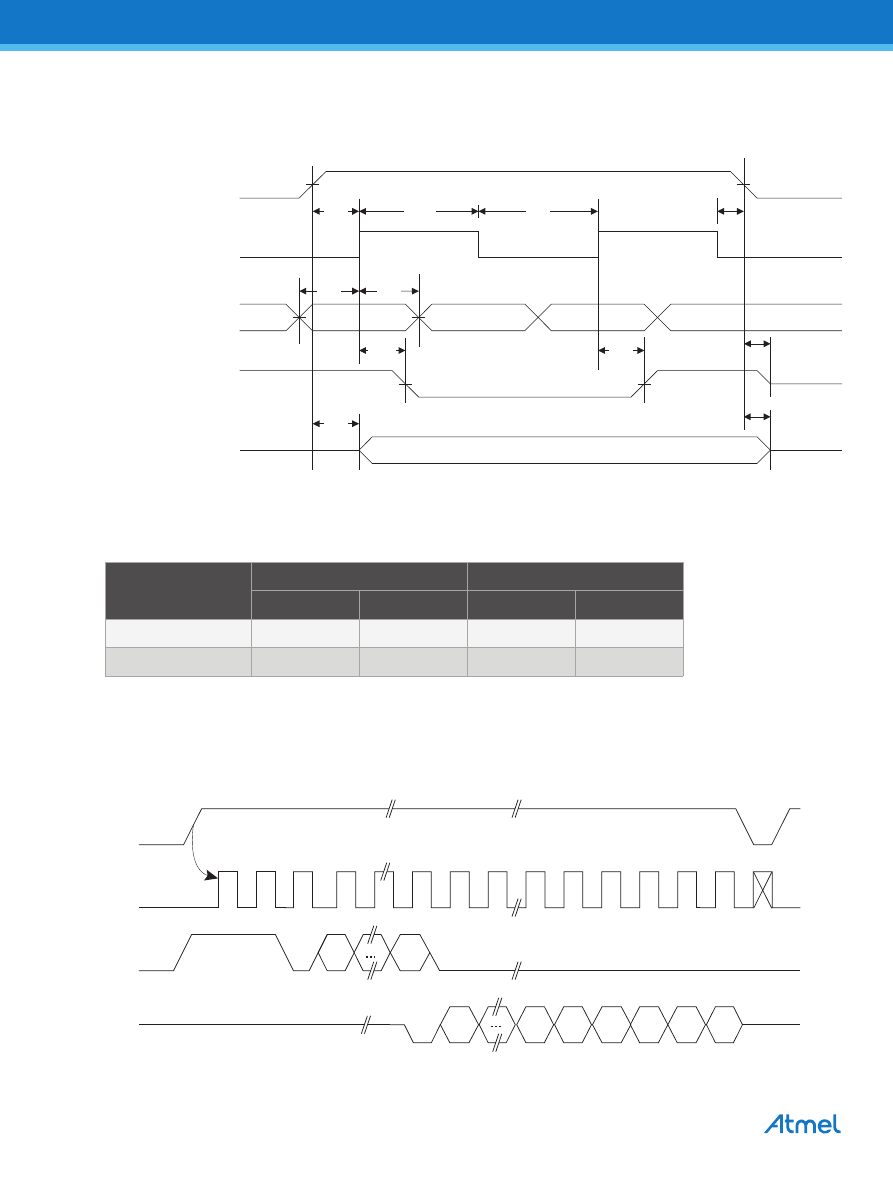
Erase/Write Enable (EWEN): To ensure data integrity, the part automatically goes into the Erase/Write Disable
(EWDS) state when power is first applied. An Erase/Write Enable (EWEN) instruction must be executed first
before any programming instructions can be carried out.
Note: Once in the EWEN state, programming remains enabled until an EWDS instruction is executed, or V
CC
power is removed from the part.
Instruction
SB Opcode
Address
Data
Comments
x8
x16
READ
1
10
A
8
- A
0
A
7
- A
0
Reads data stored in memory at
specified address.
EWEN
1
00
11XXXXXXX
11XXXXXX
Write Enable must precede all
programming modes.
ERASE
1
11
A
8
- A
0
A
7
- A
0
Erases memory location A
N
- A
0
.
WRITE
1
01
A
8
- A
0
A
7
- A
0
D
7
- D
0
D
15
- D
0
Writes memory location A
N
- A
0
.
ERAL
1
00
10XXXXXXX
10XXXXXX
Erases all memory locations.
Valid only at V
CC3
WRAL
1
00
01XXXXXXX
01XXXXXX
D
7
- D
0
D
15
- D
0
Writes all memory locations.
Valid only at V
CC3
Disable Register cleared.
EWDS
1
00
00XXXXXXX
00XXXXXX
Disables all programming
instructions.

7
AT93C56B/66B [DATASHEET]
Atmel-8735C-SEEPROM-AT93C56B-66B-Datasheet_012015
ERASE: The ERASE instruction programs all bits in the specified memory location to the Logic 1 state. The self-
timed erase cycle starts once the ERASE instruction and address are decoded. The DO pin outputs the
Ready/Busy status of the part if CS is brought high after being kept low for a minimum of t
CS
. A Logic 1 at the
DO pin indicates that the selected memory location has been erased, and the part is ready for another
instruction.
WRITE: The WRITE instruction contains the 8-bits or 16-bits of data to be written into the specified memory
location. The self-timed programming cycle, t
WP
, starts after the last bit of data is received at Serial Data Input
pin DI. The DO pin outputs the Ready/Busy status of the part if CS is brought high after being kept low for a
minimum of t
CS
. A
Logic 0 at DO indicates that programming is still in progress. A Logic 1 indicates that the memory location at the
specified address has been written with the data pattern contained in the instruction, and the part is ready for
further instructions. A Ready/Busy status cannot be obtained if CS is brought high after the end of the
self-timed programming cycle, t
WP
.
Erase All (ERAL): The Erase All (ERAL) instruction programs every bit in the Memory Array to the Logic 1 state
and is primarily used for testing purposes. The DO pin outputs the ready/busy status of the part if CS is brought
high after being kept low for a minimum of t
CS
. The ERAL instruction is valid only at
V
CC3
.
Write All (WRAL): The Write All (WRAL) instruction programs all memory locations with the data patterns
specified in the instruction. The DO pin outputs the Ready/Busy status of the part if CS is brought high after
being kept low for a minimum of t
CS
. The WRAL instruction is valid only at
V
CC3
(
Erase/Write Disable (EWDS): To protect against accidental data disturbance, the Erase/Write Disable (EWDS)
instruction disables all programming modes and should be executed after all programming operations. The
operation of the Read instruction is independent of both the EWEN and EWDS instructions and can be
executed at any time.
AT93C56B/66B [DATASHEET]
Atmel-8735C-SEEPROM-AT93C56B-66B-Datasheet_012015
8
6.
Timing Diagrams
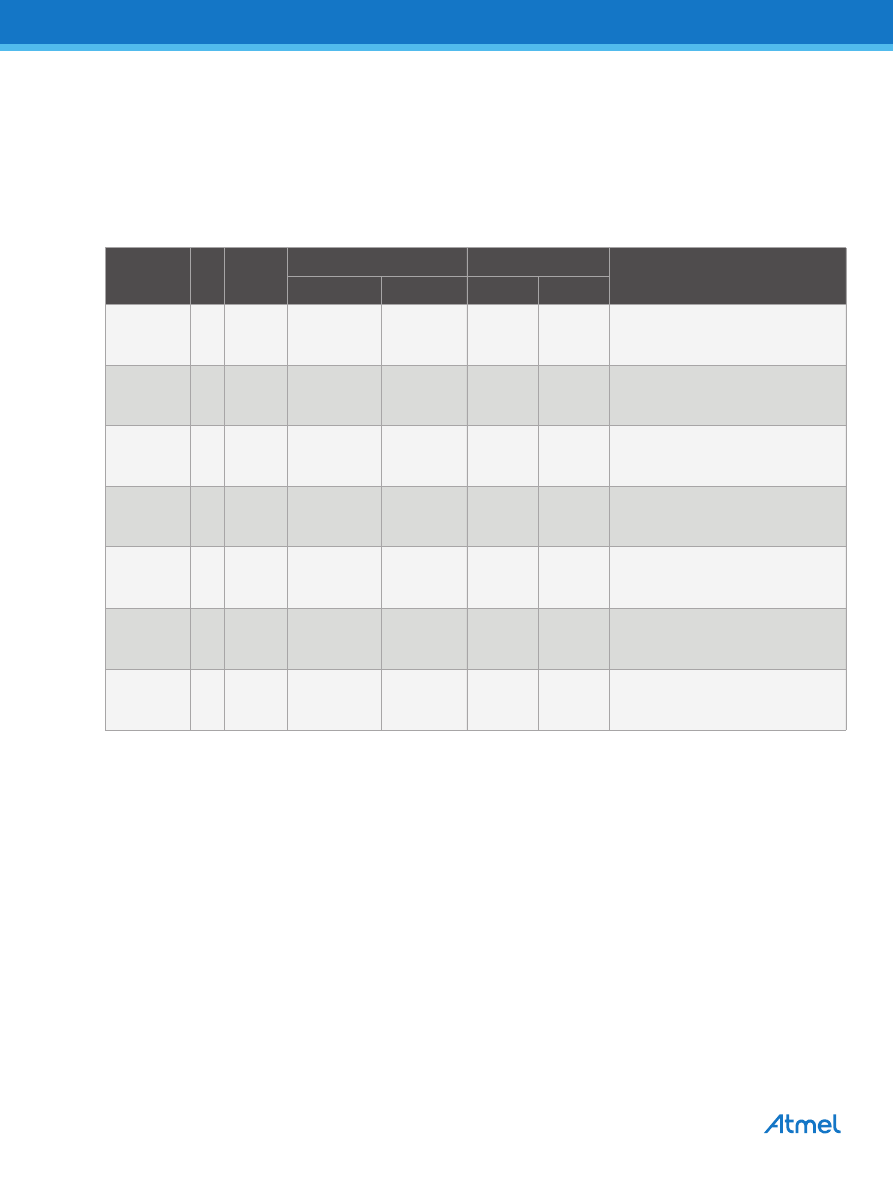
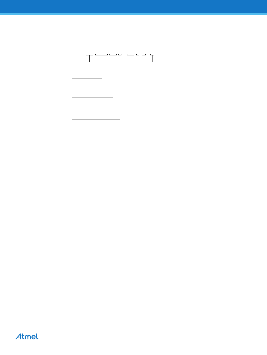
Figure 6-1.
Synchronous Data Timing
Table 6-1.
Organization Key for Timing Diagrams
Notes: 1.
A
8
is a dont-care value, but the extra clock is required.
2.
A
7
is a dont-care value, but the extra clock is required.
Figure 6-2.
READ Timing
I/O
AT93C56B (2K)
AT93C66B (4K)
x8
x16
x8
x16
A
N
A
A
A
8
A
7
D
N
D
7
D
15
D
7
D
15
CS
SK
DI
DO (Read)
DO (Program)
V
IH
V
IL
V
IH
V
IL
V
IH
V
IL
V
OH
V
OL
V
OH
V
OL
Status Valid
t
CSS
t
DIS
t
SV
t
DIH
t
PD0
t
SKH
t
SKL
t
PD1
t
CSH
t
DF
t
DF
High-impedance
CS
SK
DI
DO
1 1
0
AN
A0
0
DN
D0
t
CS
9
AT93C56B/66B [DATASHEET]
Atmel-8735C-SEEPROM-AT93C56B-66B-Datasheet_012015
Figure 6-3.
EWEN Timing
Figure 6-4.
ERASE Timing
Figure 6-5.
WRITE Timing
1
0
0
1
1
...
CS
SK
DI
t
CS
CS
SK
DI
DO
High-impedance
High-impedance
1
1
...
1
AN
t
CS
t
SV
t
DF
t
WP
AN-1 AN-2
A0
Check
Status
Standby
Ready
Busy
CS
SK
DI
t
CS
t
WP
1
1
AN
DN
0
A0
D0
...
...
DO
High-impedance
Busy
Ready
AT93C56B/66B [DATASHEET]
Atmel-8735C-SEEPROM-AT93C56B-66B-Datasheet_012015
10
Figure 6-6.
ERAL Timing
Note:
1.
Valid only at V
CC3
(
Figure 6-7.
Note:
1.
Valid only at V
CC3
(
Figure 6-8.
EWDS Timing
CS
SK
DI
DO
High-impedance
High-impedance
CS
SK
DI
DO
1
1
0
0
0
Ready
Busy
Check
Status
Standby
t
WP
t
CS
t
SV
t
DF
CS
SK
DI
DO
High-impedance
Busy
Ready
1
0
0
1
...
DN
t
CS
t
WP
...
D0
0
CS
SK
DI
DO
1
0
0
0
0
...
CS
SK
DI
t
CS
11
AT93C56B/66B [DATASHEET]
Atmel-8735C-SEEPROM-AT93C56B-66B-Datasheet_012015
7.
Ordering Code Detail
Atmel Designator
Product Family
Device Density
Device Revision
Shipping Carrier Option
Package Device Grade or
Wafer/Die Thickness
Package Option
56 = 2k
66 = 4k
93C = Microwire-compatible
3-Wire Serial EEPROM
B or Blank = Bulk (Tubes)
T = Tape and Reel, Standard Quantity Option
E = Tape and Reel, Expanded Quantity Option
Operating Voltage
M = 1.7V to 5.5V
H = Green, NiPdAu Lead Finish
Industrial Temperature Range
(-40 °C to +85 °C)
U = Green, Matte Sn Lead Finish
Industrial Temperature Range
(-40 °C to +85 °C)
11 = 11mil Wafer Thickness
SS
= JEDEC SOIC
X =
TSSOP
MA =
UDFN
ME =
XDFN
C =
VFBGA
WWU = Wafer Unsawn
A T 9 3 C 5 6 B - S S H M - B
AT93C56B/66B [DATASHEET]
Atmel-8735C-SEEPROM-AT93C56B-66B-Datasheet_012015
12
8.
Ordering Information
Note:
1.
For wafer sales, please contact Atmel sales.
Atmel Ordering Code
Lead Finish
Package
Delivery Information
Operation
Range
Form
Quantity
AT93C56B-SSHM-B
NiPdAu
(Lead-free/Halogen-free)
8S1
Bulk (Tubes)
100 per Tube
Industrial
Temperature
(-40
ï°C to 85ï°C)
AT93C56B-SSHM-T
Tape and Reel
4,000 per Reel
AT93C56B-XHM-B
8X
Bulk (Tubes)
100 per Tube
AT93C56B-XHM-T
Tape and Reel
5,000 per Reel
AT93C56B-MAHM-T
8MA2
Tape and Reel
5,000 per Reel
AT93C56B-MAHM-E
Tape and Reel
15,000 per Reel
AT93C56B-MEHM-T
8ME1
Tape and Reel
5,000 per Reel
AT93C56B-CUM-T
SnAgCu
(Lead-free/Halogen-free)
8U3-1
Tape and Reel
5,000 per Reel
N/A
Wafer Sale
AT93C66B-SSHM-B
NiPdAu
(Lead-free/Halogen-free)
8S1
Bulk (Tubes)
100 per Tube
Industrial
Temperature
(-40
ï°C to 85ï°C)
AT93C66B-SSHM-T
Tape and Reel
4,000 per Reel
AT93C66B-XHM-B
8X
Bulk (Tubes)
100 per Tube
AT93C66B-XHM-T
Tape and Reel
5,000 per Reel
AT93C66B-MAHM-T
8MA2
Tape and Reel
5,000 per Reel
AT93C66B-MAHM-E
Tape and Reel
15,000 per Reel
AT93C66B-MEHM-T
8ME1
Tape and Reel
5,000 per Reel
AT93C66B-CUM-T
SnAgCu
(Lead-free/Halogen-free)
8U3-1
Tape and Reel
5,000 per Reel
N/A
Wafer Sale
Package Type
8S1
8-lead, 0.150 wide, Plastic Gull Wing, Small Outline (JEDEC SOIC)
8X
8-lead, 0.170 wide, Thin Shrink Small Outline (TSSOP)
8MA2
8-pad, 2.00mm x 3.00mm body, 0.50mm pitch, Ultra Thin Dual No Lead (UDFN)
8ME1
8-pad, 1.80mm x 2.20mm body, Extra Thin Dual No Lead (XDFN)
8U3-1
8-ball, 1.50mm x 2.00mm body, 0.50mm pitch, Small Die Ball Grid Array (VFBGA)
13
AT93C56B/66B [DATASHEET]
Atmel-8735C-SEEPROM-AT93C56B-66B-Datasheet_012015
9.
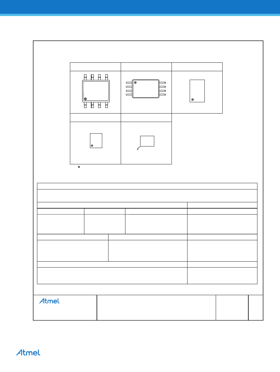
Part Markings
DRAWING NO.
REV.
TITLE
93C56-66BSM
B
3/22/13
93C56-66BSM, AT93C56B and AT93C66B Package Marking
Information
Package Mark Contact:
DL-CSO-Assy_eng@atmel.com
AAAAAAAA
###% @
ATMLHYWW
8-lead SOIC
8-lead TSSOP
AAAAAAA
###% @
ATHYWW
###
YXX
8-pad XDFN
8-pad UDFN
###
H%@
YXX
2.0 x 3.0 mm Body
1.5 x 2.0 mm Body
8-ball VFBGA
PIN 1
###U
YMXX
1.8 x 2.2 mm Body
Note 2: Package drawings are not to scale
Note 1: designates pin 1
AT93C56B and AT93C66B: Package Marking Information
Catalog Number Truncation
AT93C56B
Truncation Code ###: 56B
AT93C66B
Truncation Code ###: 66B
Date
Codes
Voltages
Y = Year
M = Month
WW = Work Week of Assembly
% = Minimum Voltage
3: 2013
7: 2017
A: January
02: Week 2
M: 1.7V min
4: 2014
8: 2018
B: February
04: Week 4
5: 2015
9: 2019
...
...
6: 2016
0: 2020
L: December
52: Week 52
Country of Assembly
Lot Number
Grade/Lead Finish Material
@ = Country of Assembly
AAA...A = Atmel Wafer Lot Number
U: Industrial/Matte Tin/SnAgCu
H: Industrial/NiPdAu
Trace
Code
Atmel Truncation
XX = Trace Code (Atmel Lot Numbers Correspond to Code)
AT: Atmel
Example: AA, AB.... YZ, ZZ
ATM: Atmel
ATML: Atmel
AT93C56B/66B [DATASHEET]
Atmel-8735C-SEEPROM-AT93C56B-66B-Datasheet_012015
14
10.
Packaging Information
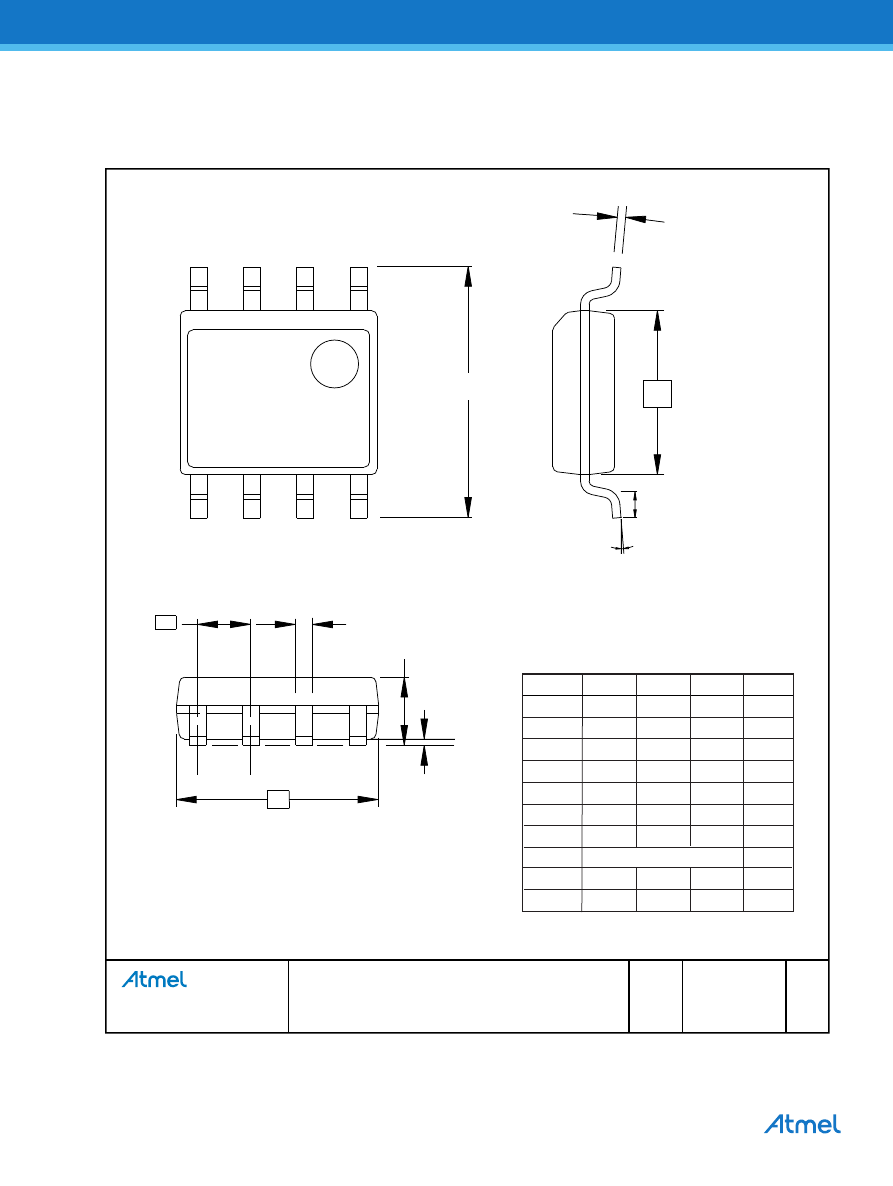
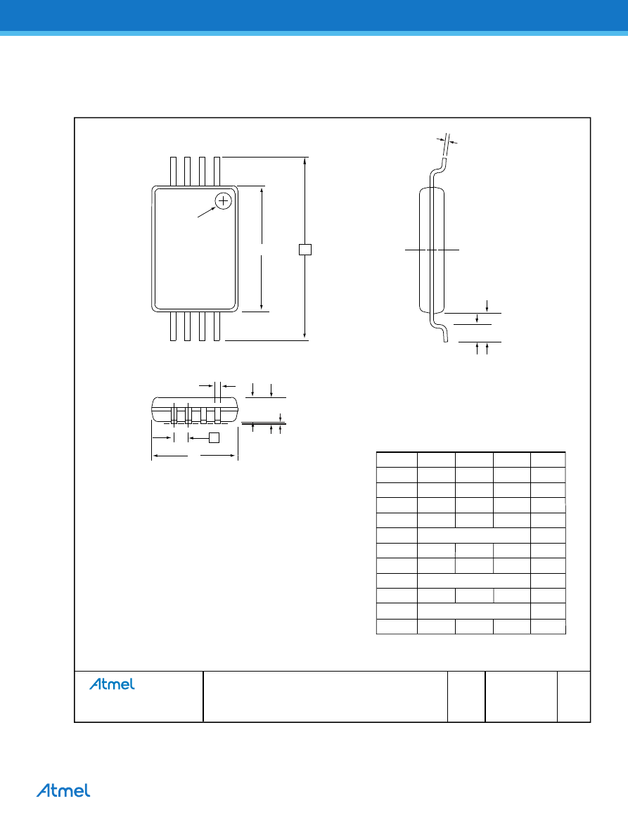
10.1 8S1 8-lead JEDEC SOIC
DRAWING NO.
REV.
TITLE
GPC
COMMON DIMENSIONS
(Unit of Measure = mm)
SYMBOL
MIN
NOM
MAX
NOTE
A1
0.10
-
0.25
A
1.35
-
1.75
b 0.31 - 0.51
C
0.17
-
0.25
D
4.80
-
5.05
E1
3.81
-
3.99
E
5.79
-
6.20
e
1.27 BSC
L 0.40 - 1.27
Ã
Ã
0 ° - 8 °
Ã
E
1
N
TOP VIEW
C
E1
END VIEW
A
b
L
A1
e
D
SIDE VIEW
Package Drawing Contact:
packagedrawings@atmel.com
8S1
G
6/22/11
Notes: This drawing is for general information only.
Refer to JEDEC Drawing MS-012, Variation AA
for proper dimensions, tolerances, datums, etc.
8S1, 8-lead (0.150 Wide Body), Plastic Gull Wing
Small Outline (JEDEC SOIC)
SWB
15
AT93C56B/66B [DATASHEET]
Atmel-8735C-SEEPROM-AT93C56B-66B-Datasheet_012015
10.2 8X 8-lead TSSOP
DRAWING NO.
REV.
TITLE
GPC
COMMON DIMENSIONS
(Unit of Measure = mm)
SYMBOL
MIN
NOM
MAX
NOTE
A - -
1.20
A1 0.05 - 0.15
A2 0.80
1.00
1.05
D 2.90
3.00
3.10
2,
5
E
6.40
BSC
E1 4.30
4.40
4.50
3,
5
b
0.19
0.25
0.30
4
e
0.65 BSC
L
0.45
0.60
0.75
L1
1.00
REF
C 0.09 -
0.20
Side View
End View
Top View
A2
A
L
L1
D
1
E1
N
b
Pin 1 indicator
this corner
E
e
Notes:
1. This drawing is for general information only.
Refer to JEDEC Drawing MO-153, Variation AA, for proper
dimensions, tolerances, datums, etc.
2. Dimension D does not include mold Flash, protrusions or gate
burrs. Mold Flash, protrusions and gate burrs shall not exceed
0.15mm (0.006in) per side.
3. Dimension E1 does not include inter-lead Flash or protrusions.
Inter-lead Flash and protrusions shall not exceed 0.25mm
(0.010in) per side.
4. Dimension b does not include Dambar protrusion.
Allowable Dambar protrusion shall be 0.08mm total in excess
of the b dimension at maximum material condition. Dambar
cannot be located on the lower radius of the foot. Minimum
space between protrusion and adjacent lead is 0.07mm.
5. Dimension D and E1 to be determined at Datum Plane H.
Package Drawing Contact:
packagedrawings@atmel.com
8X
E
2/27/14
8X, 8-lead 4.4mm Body, Plastic Thin
Shrink Small Outline Package (TSSOP)
TNR
C
A1

AT93C56B/66B [DATASHEET]
Atmel-8735C-SEEPROM-AT93C56B-66B-Datasheet_012015
16
10.3 8MA2 8-pad UDFN
DRAWING NO.
REV.
TITLE
GPC
8MA2
G
11/26/14
8MA2, 8-pad 2 x 3 x 0.6mm Body, Thermally
Enhanced Plastic Ultra Thin Dual Flat No-Lead
Package (UDFN)
YNZ
COMMON DIMENSIONS
(Unit of Measure = mm)
SYMBOL
MIN
NOM
MAX
NOTE
A
0.50
0.55
0.60
A1
0.0
0.02
0.05
A2
-
-
0.55
D
1.90
2.00
2.10
D2
1.40
1.50
1.60
E
2.90
3.00
3.10
E2
1.20
1.30
1.40
b 0.18
0.25
0.30
3
C
1.52 REF
L
0.30
0.35
0.40
e
0.50 BSC
K
0.20
-
-
TOP VIEW
SIDE VIEW
BOTTOM VIEW
Package Drawing Contact:
packagedrawings@atmel.com
C
E
Pin 1 ID
D
8
7
6
5
1
2
3
4
A
A1
A2
D2
E2
e (6x)
L (8x)
b (8x)
Pin#1 ID
K
1
2
3
4
8
7
6
5
Notes:
1. This drawing is for general information only. Refer to
Drawing MO-229, for proper dimensions, tolerances,
datums, etc.
2. The Pin #1 ID is a laser-marked feature on Top View.
3. Dimensions b applies to metallized terminal and is
measured between 0.15 mm and 0.30 mm from the
terminal tip. If the terminal has the optional radius on
the other end of the terminal, the dimension should
not be measured in that radius area.
4. The Pin #1 ID on the Bottom View is an orientation
feature on the thermal pad.
17
AT93C56B/66B [DATASHEET]
Atmel-8735C-SEEPROM-AT93C56B-66B-Datasheet_012015
10.4 8ME1 8-pad XDFN
Package Drawing Contact:
packagedrawings@atmel.com
GPC
DRAWING NO.
REV.
TITLE
COMMON DIMENSIONS
(Unit of Measure = mm)
DTP
SYMBOL
MIN
NOM
MAX
NOTE
-
0.00
1.70
2.10
0.15
0.26
A
A1
D
E
b
e
e1
L
-
-
1.80
2.20
0.20
0.40 TYP
1.20 REF
0.30
0.40
0.05
1.90
2.30
0.25
0.35
End View
8ME1
B
9/10/2012
8ME1, 8-pad (1.80mm x 2.20mm body)
Extra Thin DFN (XDFN)
Top View
6
5
7
4
3
E
D
8
1
2
PIN #1 ID
0.10
0.15
b
L
b
e
PIN #1 ID
e1
A1
A
Side View
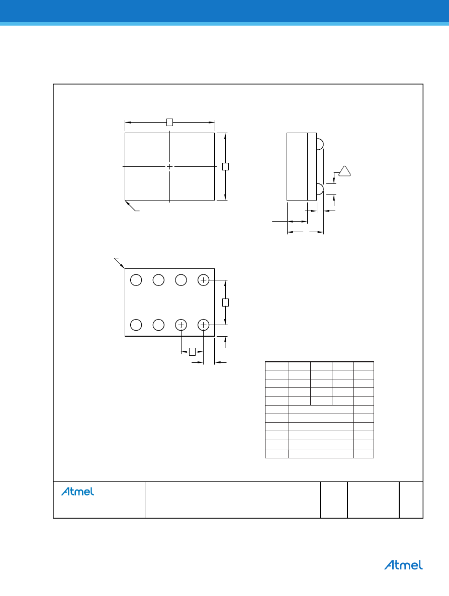
AT93C56B/66B [DATASHEET]
Atmel-8735C-SEEPROM-AT93C56B-66B-Datasheet_012015
18
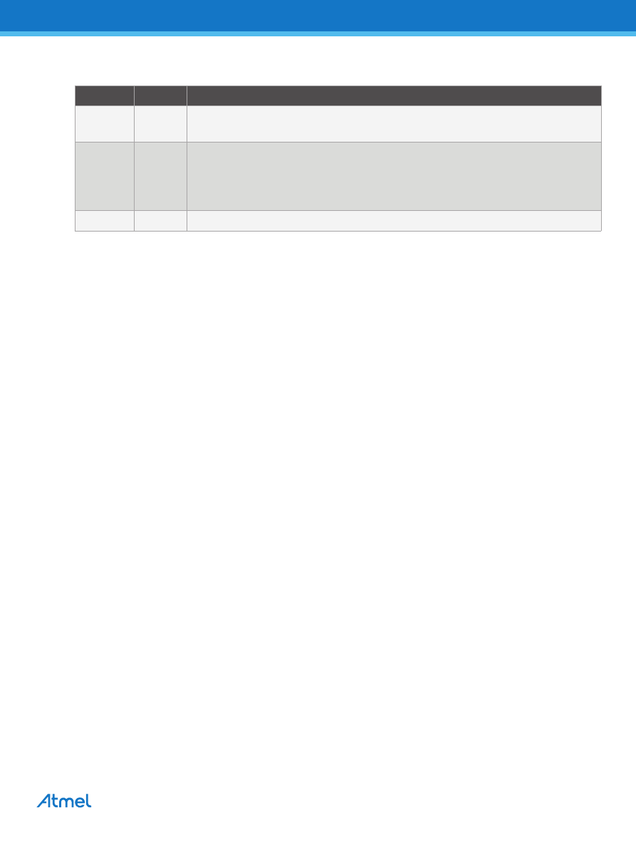
10.5 8U3-1 8-ball VFBGA
DRAWING NO.
REV.
TITLE
GPC
Package Drawing Contact:
packagedrawings@atmel.com
8U3-1
F
6/11/13
8U3-1, 8-ball, 1.50mm x 2.00mm body, 0.50mm pitch,
Very Thin, Fine-Pitch Ball Grid Array Package (VFBGA)
GXU
COMMON DIMENSIONS
(Unit of Measure - mm)
SYMBOL
MIN
NOM
MAX
NOTE
A 0.73
0.79
0.85
A1 0.09
0.14
0.19
A2 0.40
0.45
0.50
b
0.20 0.25 0.30 2
D
1.50 BSC
E
2.0 BSC
e
0.50 BSC
e1 0.25 REF
d
1.00 BSC
d1 0.25 REF
1. This drawing is for general information only.
2. Dimension b is measured at maximum solder ball diameter.
3. Solder ball composition shall be 95.5Sn-4.0Ag-.5Cu.
Notes:
A2
SIDE VIEW
A
PIN 1 BALL PAD CORNER
TOP VIEW
E
D
A1
b
8 SOLDER BALLS
BOTTOM VIEW
(d1)
d
4
3
2
(e1)
6
e
5
7
PIN 1 BALL PAD CORNER
1
8
2.
19
AT93C56B/66B [DATASHEET]
Atmel-8735C-SEEPROM-AT93C56B-66B-Datasheet_012015
11.
Revision History
Rev. No.
Date
Comments
8735C
01/2015
Add the UDFN extended quantity option and update package outline drawings.
Update the 8MA2 package drawing.
8735B
04/2013
Correct Synchronous Data Timing figure and remove note.
Update TSSOP package option from 8A2 to 8X.
Update UDFN package option from 8Y6 to 8MA2.
Update template and Atmel logos.
8735A
01/2011
Initial document release.

Atmel Corporation
1600 Technology Drive, San Jose, CA 95110 USA
T: (+1)(408) 441.0311
F: (+1)(408) 436.4200
© 2015 Atmel Corporation. / Rev.: Atmel-8735C-SEEPROM-AT93C56B-66B-Datasheet_012015.
Atmel
®
, Atmel logo and combinations thereof, Enabling Unlimited Possibilities
®
, and others are registered trademarks or trademarks of Atmel Corporation in U.S. and
other countries. Other terms and product names may be trademarks of others.
DISCLAIMER: The information in this document is provided in connection with Atmel products. No license, express or implied, by estoppel or otherwise, to any intellectual property right
is granted by this document or in connection with the sale of Atmel products. EXCEPT AS SET FORTH IN THE ATMEL TERMS AND CONDITIONS OF SALES LOCATED ON THE
ATMEL WEBSITE, ATMEL ASSUMES NO LIABILITY WHATSOEVER AND DISCLAIMS ANY EXPRESS, IMPLIED OR STATUTORY WARRANTY RELATING TO ITS PRODUCTS
INCLUDING, BUT NOT LIMITED TO, THE IMPLIED WARRANTY OF MERCHANTABILITY, FITNESS FOR A PARTICULAR PURPOSE, OR NON-INFRINGEMENT. IN NO EVENT
SHALL ATMEL BE LIABLE FOR ANY DIRECT, INDIRECT, CONSEQUENTIAL, PUNITIVE, SPECIAL OR INCIDENTAL DAMAGES (INCLUDING, WITHOUT LIMITATION, DAMAGES
FOR LOSS AND PROFITS, BUSINESS INTERRUPTION, OR LOSS OF INFORMATION) ARISING OUT OF THE USE OR INABILITY TO USE THIS DOCUMENT, EVEN IF ATMEL HAS
BEEN ADVISED OF THE POSSIBILITY OF SUCH DAMAGES. Atmel makes no representations or warranties with respect to the accuracy or completeness of the contents of this
document and reserves the right to make changes to specifications and products descriptions at any time without notice. Atmel does not make any commitment to update the information
contained herein. Unless specifically provided otherwise, Atmel products are not suitable for, and shall not be used in, automotive applications. Atmel products are not intended,
authorized, or warranted for use as components in applications intended to support or sustain life.
SAFETY-CRITICAL, MILITARY, AND AUTOMOTIVE APPLICATIONS DISCLAIMER: Atmel products are not designed for and will not be used in connection with any applications where
the failure of such products would reasonably be expected to result in significant personal injury or death (Safety-Critical Applications) without an Atmel officer's specific written
consent. Safety-Critical Applications include, without limitation, life support devices and systems, equipment or systems for the operation of nuclear facilities and weapons systems.
Atmel products are not designed nor intended for use in military or aerospace applications or environments unless specifically designated by Atmel as military-grade. Atmel products are
not designed nor intended for use in automotive applications unless specifically designated by Atmel as automotive-grade.
Document Outline

