| Secciones |
|---|
| Foros Electrónica |
|
|
| Boletines de correo |
 |

© 2004 by Catalyst Semiconductor, Inc.
Characteristics subject to change without notice.
Doc. No. 1088, Rev. M
HA
LOGEN FREE
TM
LEAD FREE
CS
SK
DI
DO
VCC
NC
ORG
GND
1
2
3
4
8
7
6
5
CS
SK
DI
DO
VCC
ORG
GND
1
2
3
4
8
7
6
5
VCC
CS
SK
ORG
GND
DO
DI
1
2
3
4
8
7
6
5
CS
SK
DI
DO
VCC
ORG
GND
1
2
3
4
8
7
6
5
NC
NC
NC
1
2
3
4
8
7
6
5
VCC
NC
ORG
GND
CS
SK
DI
DO
8
7
6
5
VCC
ORG
GND
DI
CS
SK
DO
1
2
3
4
NC
CAT93C56/57
(Die Rev. E)
2K-Bit Microwire Serial EEPROM
FEATURES
High speed operation: 1MHz
Low power CMOS technology
1.8 to 6.0 volt operation
Selectable x8 or x16 memory organization
Self-timed write cycle with auto-clear
Hardware and software write protection
Power-up inadvertant write protection
1,000,000 Program/erase cycles
100 year data retention
Commercial, industrial and automotive
temperature ranges
Sequential read
Green package option available
PIN CONFIGURATION
DIP Package (P, L)
SOIC Package (J,W)
using Catalysts advanced CMOS EEPROM floating
gate technology. The devices are designed to endure
1,000,000 program/erase cycles and has a data reten-
tion of 100 years. The devices are available in 8-pin DIP,
8-pin SOIC, 8-pin TSSOP and 8-pad TDFN packages.
DESCRIPTION
The CAT93C56/57 are 2K-bit Serial EEPROM memory
devices which are configured as either registers of 16
bits (ORG pin at V
CC
) or 8 bits (ORG pin at GND). Each
register can be written (or read) serially by using the
DI (or DO) pin. The CAT93C56/57 are manufactured
SOIC Package (S,V)
SOIC Package (K,X)
TSSOP Package (U,Y)
TDFN Package (RD4, ZD4)
Bottom View
FUNCTIONAL SYMBOL
Note: When the ORG pin is connected to VCC, the x16 organiza-
tion is selected. When it is connected to ground, the x8 pin is
selected. If the ORG pin is left unconnected, then an internal pullup
device will select the x16 organization.
CS
SK
NC
ORG
DO
DI
V
CC
GND
PIN FUNCTIONS
Pin Name
Function
CS
Chip Select
SK
Clock Input
DI
Serial Data Input
DO
Serial Data Output
V
CC
+1.8 to 6.0V Power Supply
GND
Ground
ORG
Memory Organization
NC
No Connection
2
CAT93C56/57
Doc. No. 1088, Rev. M
D.C. OPERATING CHARACTERISTICS
V
CC
= +1.8V to +6.0V, unless otherwise specified.
SymbolParameter
Test Conditions
Min
Typ
Max
Units
I
CC1
Power Supply Current
f
SK
= 1MHz
3
mA
(Write)
V
CC
= 5.0V
I
CC2
Power Supply Current
f
SK
= 1MHz
500
µA
(Read)
V
CC
= 5.0V
I
SB1
Power Supply Current
CS = 0V
10
µA
(Standby) (x8 Mode)
ORG=GND
I
SB2
Power Supply Current
CS=0V
0
10
µA
(Standby) (x16Mode)
ORG=Float or V
CC
I
LI
Input Leakage Current
V
IN
= 0V to V
CC
1
µA
I
LO
Output Leakage Current
V
OUT
= 0V to V
CC
,
1
µA
(Including ORG pin)
CS = 0V
V
IL1
Input Low Voltage
4.5V
≤ V
CC
< 5.5V
-0.1
0.8
V
V
IH1
Input High Voltage
4.5V
≤ V
CC
< 5.5V
2
V
CC
+ 1
V
V
IL2
Input Low Voltage
1.8V
≤ V
CC
< 4.5V
0
V
CC
x 0.2
V
V
IH2
Input High Voltage
1.8V
≤ V
CC
< 4.5V
V
CC
x 0.7
V
CC
+1
V
V
OL1
Output Low Voltage
4.5V
≤ V
CC
< 5.5V
0.4
V
I
OL
= 2.1mA
V
OH1
Output High Voltage
4.5V
≤ V
CC
< 5.5V
2.4
V
I
OH
= -400
µA
V
OL2
Output Low Voltage
1.8V
≤ V
CC
< 4.5V
0.2
V
I
OL
= 1mA
V
OH2
Output High Voltage
1.8V
≤ V
CC
< 4.5V
V
CC
- 0.2
V
I
OH
= -100
µA
ABSOLUTE MAXIMUM RATINGS*
Temperature Under Bias .................. -55
°C to +125 °C
Storage Temperature ........................ -65
°C to +150 °C
Voltage on any Pin with
Respect to Ground
(1)
............. -2.0V to +V
CC
+2.0V
V
CC
with Respect to Ground ................ -2.0V to +7.0V
Package Power Dissipation
Capability (T
A
= 25
°C) ................................... 1.0W
Lead Soldering Temperature (10 secs) ............ 300
°C
Output Short Circuit Current
(2)
........................ 100 mA
*COMMENT
Stresses above those listed under Absolute Maximum
Ratings may cause permanent damage to the device.
These are stress ratings only, and functional operation of
the device at these or any other conditions outside of those
listed in the operational sections of this specification is not
implied. Exposure to any absolute maximum rating for
extended periods may affect device performance and
reliability.
RELIABILITY CHARACTERISTICS
SymbolParameter
Reference Test Method
Min
Typ
Max
Units
N
END
(3)
Endurance
MIL-STD-883, Test Method 1033
1,000,000
Cycles/Byte
T
DR
(3)
Data Retention
MIL-STD-883, Test Method 1008
100
Years
V
ZAP
(3)
ESD Susceptibility
MIL-STD-883, Test Method 3015
2000
Volts
I
LTH
(3)(4)
Latch-Up
JEDEC Standard 17
100
mA
Note:
(1) The minimum DC input voltage is -0.5V. During transitions, inputs may undershoot to -2.0V for periods of less than 20 ns. Maximum DC
voltage on output pins is V
CC
+0.5V, which may overshoot to V
CC
+2.0V for periods of less than 20 ns.
(2) Output shorted for no more than one second. No more than one output shorted at a time.
(3) This parameter is tested initially and after a design or process change that affects the parameter.
(4) Latch-up protection is provided for stresses up to 100 mA on address and data pins from -1V to V
CC
+1V.
3
CAT93C56/57
Doc. No. 1088, Rev. M
PIN CAPACITANCE
SymbolTest
Conditions
Min
Typ
Max
Units
C
OUT
(2)
Output Capacitance (DO)
V
OUT
=0V
5
pF
C
IN
(2)
Input Capacitance (CS, SK, DI, ORG)
V
IN
=0V
5
pF
INSTRUCTION SET
n
o
i
t
c
u
r
t
s
n
I
e
c
i
v
e
D
e
p
y
T
t
r
a
t
S
t
i
B
e
d
o
c
p
O
s
s
e
r
d
d
A
a
t
a
D
s
t
n
e
m
m
o
C
8
x
6
1
x
8
x
6
1
x
D
A
E
R
6
5
C
3
9
)
1
(
1
0
1
0
A
-
8
A
0
A
-
7
A
0
A
-
N
A
s
s
e
r
d
d
A
d
a
e
R
7
5
C
3
9
1
0
1
0
A
-
7
A
0
A
-
6
A
E
S
A
R
E
6
5
C
3
9
)
1
(
1
1
1
0
A
-
8
A
0
A
-
7
A
0
A
-
N
A
s
s
e
r
d
d
A
r
a
e
l
C
7
5
C
3
9
1
1
1
0
A
-
7
A
0
A
-
6
A
E
T
I
R
W
6
5
C
3
9
)
1
(
1
1
0
0
A
-
8
A
0
A
-
7
A
0
D
-
7
D
0
D
-
5
1
D
0
A
-
N
A
s
s
e
r
d
d
A
e
t
i
r
W
7
5
C
3
9
1
1
0
0
A
-
7
A
0
A
-
6
A
0
D
-
7
D
0
D
-
5
1
D
N
E
W
E
6
5
C
3
9
)
1
(
1
0
0
X
X
X
X
X
1
1
X
X
X
X
X
X
X
1
1
X
e
l
b
a
n
E
e
t
i
r
W
7
5
C
3
9
1
0
0
X
X
X
X
X
1
1
X
X
X
X
X
X
1
1
S
D
W
E
6
5
C
3
9
)
1
(
1
0
0
0
0
X
X
X
X
X
X
X
0
0
X
X
X
X
X
X
e
l
b
a
s
i
D
e
t
i
r
W
7
5
C
3
9
1
0
0
0
0
X
X
X
X
X
X
0
0
X
X
X
X
X
L
A
R
E
6
5
C
3
9
)
1
(
1
0
0
10
X
X
X
X
X
X
X
10
X
X
X
X
X
X
s
e
s
s
e
r
d
d
A
ll
A
r
a
e
l
C
7
5
C
3
9
1
0
0
10
X
X
X
X
X
X
10
X
X
X
X
X
L
A
R
W
6
5
C
3
9
)
1
(
1
0
0
0
X
X
X
X
X
1
X
X
0
X
X
X
X
X
1
X
0
D
-
7
D
0
D
-
5
1
D
s
e
s
s
e
r
d
d
A
ll
A
e
t
i
r
W
7
5
C
3
9
1
0
0
0
X
X
X
X
X
1
X
0
X
X
X
X
X
1
0
D
-
7
D
0
D
-
5
1
D
Limits
V
CC
=
V
CC
=
V
CC
=
1.8V-6V
2.5V-6V
4.5V-5.5V
Test
SymbolParameter
Conditions
Min
Max
Min
Max
Min
Max
Units
t
CSS
CS Setup Time
200
100
50
ns
t
CSH
CS Hold Time
0
0
0
ns
t
DIS
DI Setup Time
400
200
100
ns
t
DIH
DI Hold Time
400
200
100
ns
t
PD1
Output Delay to 1
1
0.5
0.25
µs
t
PD0
Output Delay to 0
1
0.5
0.25
µs
t
HZ
(1)
Output Delay to High-Z
400
200
100
ns
t
EW
Program/Erase Pulse Width
10
10
10
ms
t
CSMIN
Minimum CS Low Time
1
0.5
0.25
µs
t
SKHI
Minimum SK High Time
1
0.5
0.25
µs
t
SKLOW
Minimum SK Low Time
1
0.5
0.25
µs
t
SV
Output Delay to Status Valid
1
0.5
0.25
µs
SK
MAX
Maximum Clock Frequency
DC
250
DC
500
DC
1000
kHz
A.C. CHARACTERISTICS
C
L
= 100pF
(3)
Note:
(1)
Address bit A8 for 256x8 ORG and A7 for 128x16 ORG are "Don't Care" bits, but must be kept at either a "1" or "0" for READ, WRITE
and ERASE commands.
(2)
This parameter is tested initially and after a design or process change that affects the parameter.
4
CAT93C56/57
Doc. No. 1088, Rev. M
A.C. TEST CONDITIONS
Input Rise and Fall Times
≤ 50ns
Input Pulse Voltages
0.4V to 2.4V
4.5V
≤ V
CC
≤ 5.5V
Timing Reference Voltages
0.8V, 2.0V
4.5V
≤ V
CC
≤ 5.5V
Input Pulse Voltages
0.2V
CC
to 0.7V
CC
1.8V
≤ V
CC
≤ 4.5V
Timing Reference Voltages
0.5V
CC
1.8V
≤ V
CC
≤ 4.5V
POWER-UP TIMING
(1)(2)
SymbolParameter
Max
Units
t
PUR
Power-up to Read Operation
1
ms
t
PUW
Power-up to Write Operation
1
ms
NOTE:
(1) This parameter is tested initially and after a design or process change that affects the parameter.
(2) t
PUR
and t
PUW
are the delays required from the time V
CC
is stable until the specified operation can be initiated.
(3) The input levels and timing reference points are shown in AC Test Conditions table.
DEVICE OPERATION
The CAT93C56/57 is a 2048-bit nonvolatile memory
intended for use with industry standard microproces-
sors. The CAT93C56/57 can be organized as either
registers of 16 bits or 8 bits. When organized as X16,
seven 10-bit instructions for 93C57; seven 11-bit
instructions for 93C56 control the reading, writing and
erase operations of the device. When organized as X8,
seven 11-bit instructions for 93C57; seven 12-bit in-
structions for 93C56 control the reading, writing and
erase operations of the device. The CAT93C56/57
operates on a single power supply and will generate
on chip, the high voltage required during any write
operation.
Instructions, addresses, and write data are clocked into
the DI pin on the rising edge of the clock (SK). The DO
pin is normally in a high impedance state except when
reading data from the device, or when checking the
ready/busy status after a write operation.
The ready/busy status can be determined after the start
of a write operation by selecting the device (CS high)
and polling the DO pin; DO low indicates that the
write operation is not completed, while DO high indi-
cates that the device is ready for the next instruction. If
necessary, the DO pin may be placed back into a high
impedance state during chip select by shifting a dummy
1 into the DI pin. The DO pin will enter the high
impedance state on the falling edge of the clock (SK).
Placing the DO pin into the high impedance state is
recommended in applications where the DI pin and the
DO pin are to be tied together to form a common DI/O
pin.
The format for all instructions sent to the device is a
logical "1" start bit, a 2-bit (or 4-bit) opcode, 7-bit address
(93C57)/ 8-bit address (93C56) (an additional bit when
organized X8) and for write operations a 16-bit data field
(8-bit for X8 organizations).
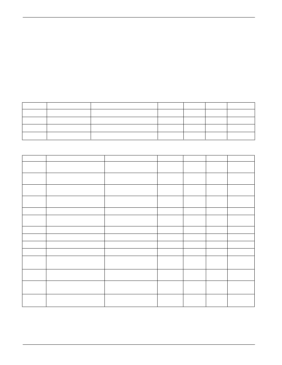
Read
Upon receiving a READ command and an address
(clocked into the DI pin), the DO pin of the CAT93C56/
57 will come out of the high impedance state and, after
sending an initial dummy zero bit, will begin shifting out
the data addressed (MSB first). The output data bits will
toggle on the rising edge of the SK clock and are stable
after the specified time delay (t
PD0
or t
PD1
).
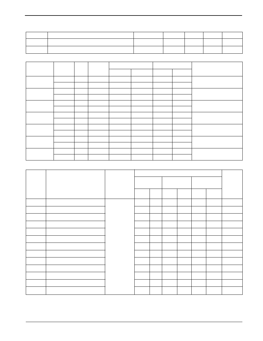
Write
After receiving a WRITE command, address and the
data, the CS (Chip Select) pin must be deselected for a
minimum of t
CSMIN
. The falling edge of CS will start the
self clocking clear and data store cycle of the memory
location specified in the instruction. The clocking of the
SK pin is not necessary after the device has entered the
self clocking mode. The ready/busy status of the
CAT93C56/57 can be determined by selecting the device
and polling the DO pin. Since this device features Auto-
Clear before write, it is NOT necessary to erase a
memory location before it is written into.
5
CAT93C56/57
Doc. No. 1088, Rev. M
Figure 1. Sychronous Data Timing
Figure 2. Read Instruction Timing
SK
DI
CS
DO
tDIS
tPD0,tPD1
tCSMIN
tCSS
tDIS
tDIH
tSKHI
tCSH
VALID
VALID
DATA VALID
tSKLOW
SK
CS
DI
DO
HIGH-Z
1
1
0
AN AN-1
A0
Dummy 0
D15 . . . D0
or
D7 . . . D0
1
1
1
1
1
1
1
1
1
1
1
1
1
1
1
Address + 1
D15 . . . D0
or
D7 . . . D0
Address + 2
D15 . . . D0
or
D7 . . . D0
Address + n
D15 . . .
or
D7 . . .
Don't Care
Figure 3. Write Instruction Timing
SK
CS
DI
DO
tCSMIN
STANDBY
HIGH-Z
HIGH-Z
1
0
1
AN AN-1
A0
DN
D0
BUSY
READY
STATUS
VERIFY
tSV
tHZ
tEW
6
CAT93C56/57
Doc. No. 1088, Rev. M
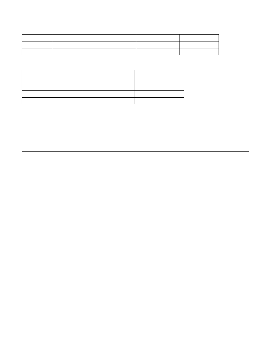
Erase
Upon receiving an ERASE command and address, the
CS (Chip Select) pin must be deasserted for a minimum
of t
CSMIN
. The falling edge of CS will start the self clocking
clear cycle of the selected memory location. The clocking
of the SK pin is not necessary after the device has
entered the self clocking mode. The ready/busy status of
the CAT93C56/57 can be determined by selecting the
device and polling the DO pin. Once cleared, the content
of a cleared location returns to a logical 1 state.
Erase/Write Enable and Disable
The CAT93C56/57 powers up in the write disable state.
Any writing after power-up or after an EWDS (write
disable) instruction must first be preceded by the EWEN
(write enable) instruction. Once the write instruction is
enabled, it will remain enabled until power to the device
is removed, or the EWDS instruction is sent. The EWDS
instruction can be used to disable all CAT93C56/57
write and clear instructions, and will prevent any
accidental writing or clearing of the device. Data can be
read normally from the device regardless of the write
enable/disable status.
Erase All
Upon receiving an ERAL command, the CS (Chip Select)
pin must be deselected for a minimum of t
CSMIN
. The
falling edge of CS will start the self clocking clear cycle
of all memory locations in the device. The clocking of the
SK pin is not necessary after the device has entered the
self clocking mode. The ready/busy status of the
CAT93C56/57 can be determined by selecting the device
and polling the DO pin. Once cleared, the contents of all
memory bits return to a logical 1 state.
Write All
Upon receiving a WRAL command and data, the CS
(Chip Select) pin must be deselected for a minimum of
t
CSMIN
. The falling edge of CS will start the self clocking
data write to all memory locations in the device. The
clocking of the SK pin is not necessary after the device
has entered the self clocking mode. The ready/busy
status of the CAT93C56/57 can be determined by
selecting the device and polling the DO pin. It is not
necessary for all memory locations to be cleared before
the WRAL command is executed.
Figure 4. Erase Instruction Timing
SK
CS
DI
DO
STANDBY
HIGH-Z
HIGH-Z
1
AN
AN-1
BUSY
READY
STATUS VERIFY
tSV
tHZ
tEW
tCS
1
1
A0
7
CAT93C56/57
Doc. No. 1088, Rev. M
Figure 7. WRAL Instruction Timing
Figure 5. EWEN/EWDS Instruction Timing
Figure 6. ERAL Instruction Timing
SK
CS
DI
STANDBY
1
0
0
*
* ENABLE=11
DISABLE=00
SK
CS
DI
DO
STANDBY
tCS
HIGH-Z
HIGH-Z
1
0
1
BUSY
READY
STATUS VERIFY
tSV
tHZ
tEW
0
0
STATUS VERIFY
SK
CS
DI
DO
STANDBY
HIGH-Z
1
0
1
BUSY
READY
tSV
tHZ
tEW
tCSMIN
DN
D0
0
0
8
CAT93C56/57
Doc. No. 1088, Rev. M
ORDERING INFORMATION
Notes:
(1) The device used in the above example is a 93C56SI-1.8TE13 (SOIC, Industrial Temperature, 1.8 Volt to 6 Volt Operating Voltage,
Tape & Reel)
(2) Product die revision letter is marked on top of the package as a suffix to the production date code (e.g., AYWWE.) For additional
information, please contact your Catalyst sales office.
Package
P = PDIP
S = SOIC (JEDEC)
J = SOIC (JEDEC)
K = SOIC (EIAJ)
U = TSSOP
RD4 = TDFN (3x3mm)
ZD4 = TDFN (3x3mm, Lead free, Halogen free)
L = PDIP (Lead free, Halogen free)
V = SOIC, JEDEC (Lead free, Halogen free)
W = SOIC, JEDEC (Lead free, Halogen free)
X = SOIC, EIAJ (Lead free, Halogen free)
Y = TSSOP (Lead free, Halogen free)
Prefix
Device #
Suffix
93C56
S
I
TE13
Product
Number
93C56: 2K
93C57: 2K
Tape & Reel
-1.8
CAT
Temperature Range
Blank = Commercial (0
°C - 70 °C)
I = Industrial (-40
°C - 85 °C)
A = Automotive (-40
°C - 105 °C)
Operating Voltage
Blank (V
cc
=2.5 to 6.0V)
1.8 (V
cc
=1.8 to 6.0V)
Optional
Company ID
E = Extended (-40
°C to + 125 °C)
Die Revision
93C56: E
93C57: E
Rev E
(2)
Copyrights, Trademarks and Patents
Trademarks and registered trademarks of Catalyst Semiconductor include each of the following:
DPP ™
AE
2
™
Catalyst Semiconductor has been issued U.S. and foreign patents and has patent applications pending that protect its products. For a complete list of patents
issued to Catalyst Semiconductor contact the Companys corporate office at 408.542.1000.
CATALYST SEMICONDUCTOR MAKES NO WARRANTY, REPRESENTATION OR GUARANTEE, EXPRESS OR IMPLIED, REGARDING THE SUITABILITY OF ITS
PRODUCTS FOR ANY PARTICULAR PURPOSE, NOR THAT THE USE OF ITS PRODUCTS WILL NOT INFRINGE ITS INTELLECTUAL PROPERTY RIGHTS OR THE
RIGHTS OF THIRD PARTIES WITH RESPECT TO ANY PARTICULAR USE OR APPLICATION AND SPECIFICALLY DISCLAIMS ANY AND ALL LIABILITY ARISING
OUT OF ANY SUCH USE OR APPLICATION, INCLUDING BUT NOT LIMITED TO, CONSEQUENTIAL OR INCIDENTAL DAMAGES.
Catalyst Semiconductor products are not designed, intended, or authorized for use as components in systems intended for surgical implant into the body, or
other applications intended to support or sustain life, or for any other application in which the failure of the Catalyst Semiconductor product could create a
situation where personal injury or death may occur.
Catalyst Semiconductor reserves the right to make changes to or discontinue any product or service described herein without notice. Products with data sheets
labeled "Advance Information" or "Preliminary" and other products described herein may not be in production or offered for sale.
Catalyst Semiconductor advises customers to obtain the current version of the relevant product information before placing orders. Circuit diagrams illustrate
typical semiconductor applications and may not be complete.
Catalyst Semiconductor, Inc.
Corporate Headquarters
1250 Borregas Avenue
Sunnyvale, CA 94089
Phone: 408.542.1000
Fax: 408.542.1200
www.catalyst-semiconductor.com
Publication #:
1088
Revison:
M
Issue date:
10/7/04
REVISION HISTORY
e
t
a
D
n
o
i
s
i
v
e
R
s
t
n
e
m
m
o
C
4
0
/
4
1
/
5
0
L
s
t
r
a
P
.
6
8
/
6
6
/
7
5
/
6
5
/
6
4
C
3
9
T
A
C
m
o
r
F
d
e
t
a
e
r
C
t
e
e
h
S
a
t
a
D
w
e
N
d
n
a
6
7
C
3
9
T
A
C
,
6
6
C
3
9
T
A
C
,
7
5
C
3
9
T
A
C
,
6
5
C
3
9
T
A
C
,
6
5
C
3
9
T
A
C
s
t
e
e
h
s
a
t
a
d
e
l
g
n
i
s
o
t
n
i
d
e
t
a
t
r
a
p
e
s
n
e
e
b
e
v
a
h
6
8
C
3
9
T
A
C
4
0
/
7
/
0
1
M
t
e
S
n
o
i
t
c
u
r
t
s
n
I
d
e
t
a
d
p
U

