| Secciones |
|---|
| Foros Electrónica |
|
|
| Boletines de correo |
 |
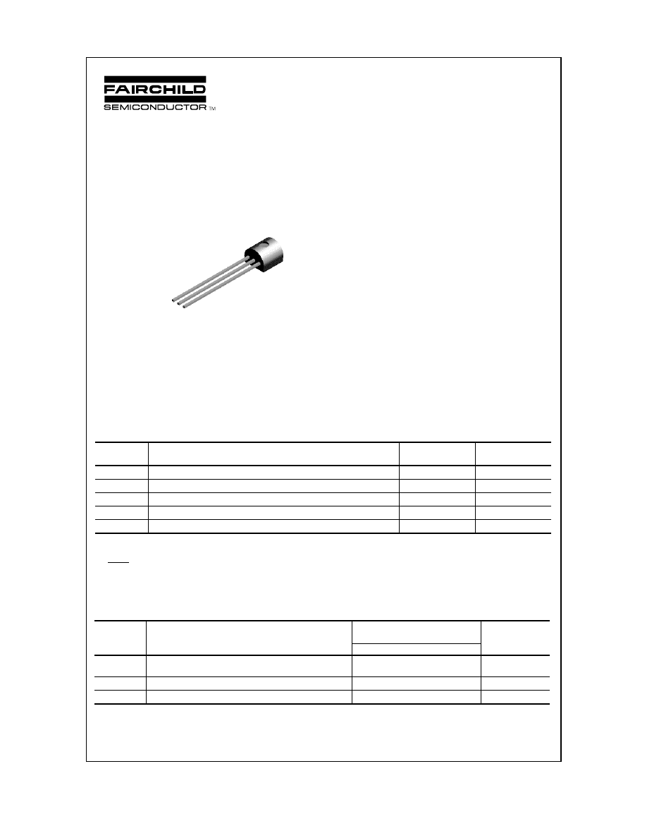
BF244A
BF244B
BF244C
N-Channel RF Amplifier
This device is designed for RF amplifier and mixer applications
operating up to 450 MHz, and for analog switching requiring low
capacitance. Sourced from Process 50.
Absolute Maximum Ratings*
TA = 25 °C unless otherwise noted
*
These ratings are limiting values above which the serviceability of any semiconductor device may be impaired.
NOTES:
1) These ratings are based on a maximum junction temperature of 150 degrees C.
2) These are steady state limits. The factory should be consulted on applications involving pulsed or low duty cycle operations.
Thermal Characteristics
TA = 25 °C unless otherwise noted
Symbol
Characteristic
Max
Units
BF244A / BF244B / BF244C
P
D
Total Device Dissipation
Derate above 25
°
C
350
2.8
mW
mW/
°
C
R
Θ
JC
Thermal Resistance, Junction to Case
125
°
C/W
R
Θ
JA
Thermal Resistance, Junction to Ambient
357
°
C/W
Symbol
Parameter
Value
Units
V
DG
Drain-Gate Voltage
30
V
V
GS
Gate-Source Voltage
- 30
V
I
D
Drain Current
50
mA
I
GF
Forward Gate Current
10
mA
T
stg
Storage Temperature Range
-55 to +150
°
C
S
G
D
TO-92

1997 Fairchild Semiconductor Corporation
BF244A / BF244B / BF244C
5
Electrical Characteristics
TA = 25 °C unless otherwise noted
OFF CHARACTERISTICS
Symbol
Parameter
Test Conditions
Min
Typ
Max Units
ON CHARACTERISTICS
I
DSS
Zero-Gate Voltage Drain Current
V
DS
= 15 V, V
GS
= 0
244A
244B
244C
2.0
6.0
12
6.5
15
25
mA
mA
mA
SMALL SIGNAL CHARACTERISTICS
y
fs
Forward Transfer Admittance
V
DS
= 15 V, V
GS
= 0, f = 1.0 kHz
V
DS
= 15 V, V
GS
= 0, f = 200 MHz
3.0
5.6
6.5
mmhos
mmhos
y
os
Output Admittance
V
DS
= 15 V, V
GS
= 0, f = 1.0 kHz
40
µ
mhos
y
rs
Reverse Transfer Admittance
V
DS
= 15 V, V
GS
= 0, f = 200 MHz
1.0
µ
mhos
C
iss
Input Capacitance
V
DS
= 20 V, V
GS
= - 1.0 V
3.0
pF
C
rss
Reverse Transfer Capacitance
V
DS
= 20 V, V
GS
= - 1.0 V,
f = 1.0 MHz
0.7
pF
C
oss
Output Capacitance
V
DS
= 20 V, V
GS
= - 1.0 V,
f = 1.0 MHz
0.9
pF
NF
Noise Figure
V
DS
= 15 V, V
GS
= 0, R
G
= 1.0 k
Ω¦
,
f = 100 MHz
1.5
dB
F(Y
fs
)
Cut-Off Frequency
V
DS
= 15 V, V
GS
= 0
700
MHz
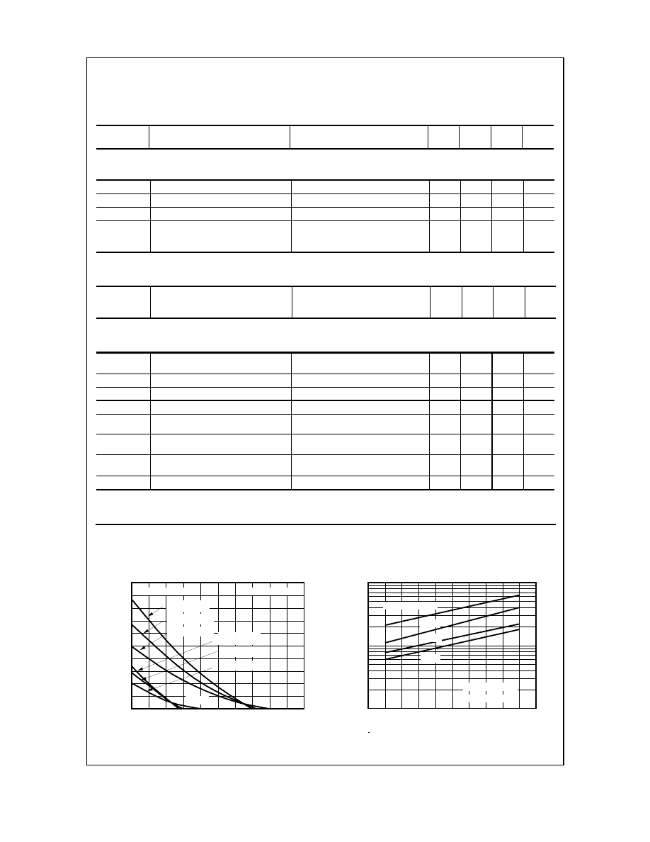
Typical Characteristics
V
(BR)GSS
Gate-Source Breakdown Voltage
I
G
= 1.0
µ
A, V
DS
= 0
30
V
I
GSS
Gate Reverse Current
V
GS
= - 20 V, V
DS
= 0
5.0
nA
V
GSS(off)
Gate-Source Cutoff Voltage
V
DS
= 15 V, I
D
= 10 nA
- 0.5
- 8.0
V
V
GS
Gate-Source Voltage
V
DS
= 15 V, I
D
= 200
µ
A
244A
244B
244C
- 0.4
- 1.6
- 3.2
- 2.2
- 3.8
- 7.5
V
V
V
Transfer Characteristics
-5
-4
-3
-2
-1
0
0
4
8
12
16
20
V - GATE-SOURCE VOLTAGE(V)
I
- DR
AI
N
C
U
R
R
E
N
T
(
m
A
)
D
GS(OFF)
V = -4.5V
V = 15V
DS
T = +25 C
A
O
-2.5 V
T = -55 C
O
A
T = +125 C
A
O
T = -55 C
O
A
T = +25 C
A
O
T = +125 C
A
O
GS
Channel Resistance vs Temperature
-50
0
50
100
150
10
20
30
50
100
200
300
500
1000
T - AMBIENT TEMPERATURE ( C)
r
-
DR
A
IN
O
N
RE
S
IS
T
A
NCE
(
)
Ω¦
V = -1.0V
GS(OFF)
-2.5 V
-5.0V
-8.0 V
V = 100mV
DS
V = 0 V
GS
DS
A
BF244A / BF244B / BF244C
N-Channel RF Amplifier
(continued)

