| Secciones |
|---|
| Foros Electrónica |
|
|
| Boletines de correo |
 |
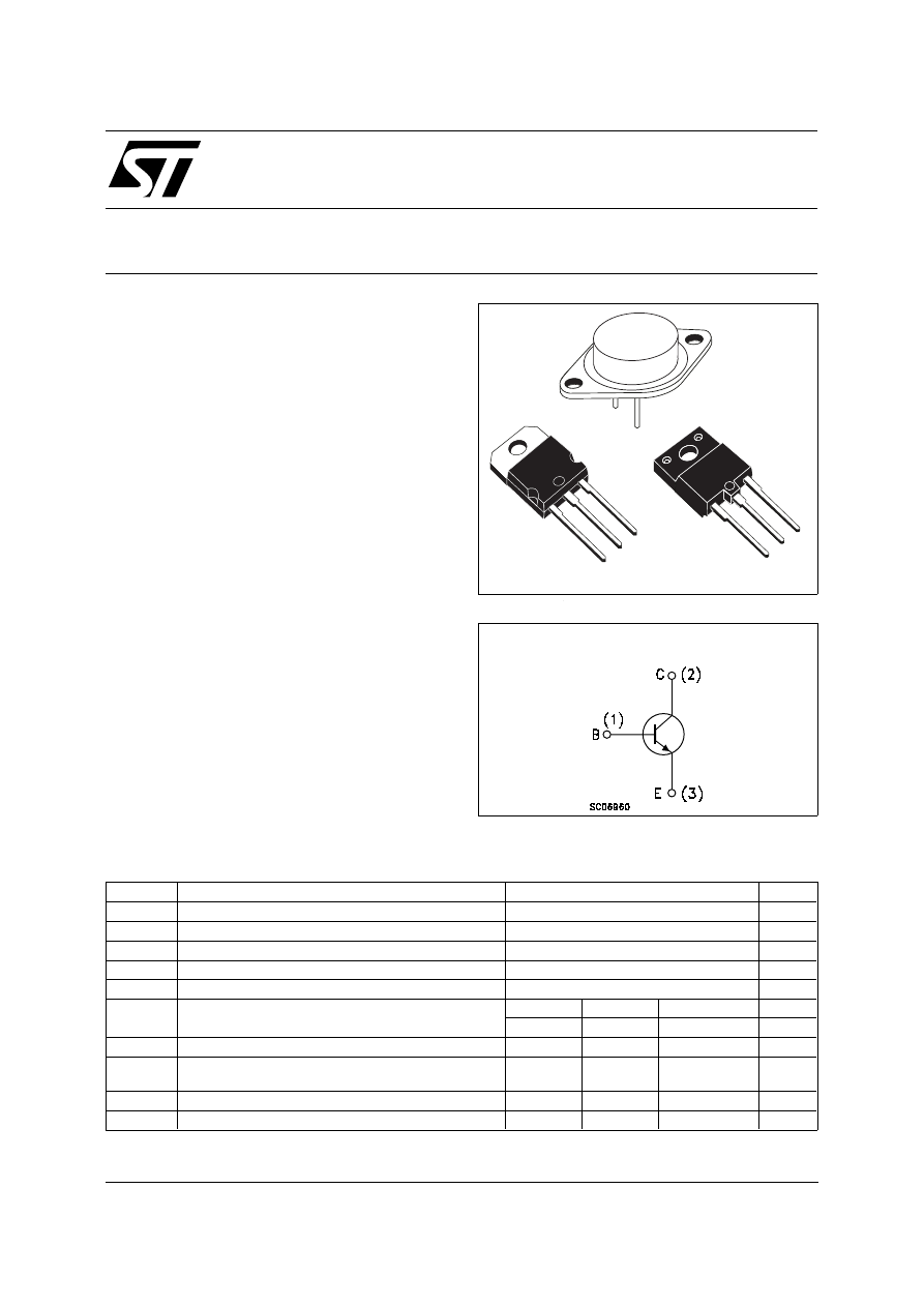
BU208A
BU508A/BU508AFI
HIGH VOLTAGE FAST-SWITCHING
NPN POWER TRANSISTORS
STMicroelectronics PREFERRED
SALESTYPES
HIGH VOLTAGE CAPABILITY (> 1500 V)
FULLY INSULATED PACKAGE (U.L.
COMPLIANT) FOR EASY MOUNTING
APPLICATIONS:
HORIZONTAL DEFLECTION FOR COLOUR
TV
DESCRIPTION
The BU208A, BU508A and BU508AFI are
manufactured using Multiepitaxial Mesa
technology for cost-effective high performance
and use a Hollow Emitter structure to enhance
switching speeds.
INTERNAL SCHEMATIC DIAGRAM
April 2002
ABSOLUTE MAXIMUM RATINGS
Symbol
Parameter
Value
Unit
V
CES
Collector-Emitter Voltage (V
BE
= 0)
1500
V
V
CEO
Collector-Emitter Voltage (I
B
= 0)
700
V
V
EBO
Emitter-Base Voltage (I
C
= 0)
10
V
I
C
Collector Current
8
A
I
CM
Collector Peak Current (t
p
< 5 ms)
15
A
BU208A
BU508A
BU508AFI
TO - 3
TO - 218
ISOWATT218
P
tot
Total Dissipation at T
c
= 25
o
C
150
125
50
W
V
isol
Insulation Withstand Voltage (RMS) from All
Three Leads to Exernal Heatsink
2500
V
T
stg
Storage Temperature
-65 to 175 -65 to 150
-65 to 150
o
C
T
j
Max. Operating Junction Temperature
175
150
150
o
C
1
2
3
TO-218 ISOWATT218
1
2
3
1
2
TO-3
For TO-3 :
C = Tab
E = Pin2.
®
1/8
THERMAL DATA
TO-3
TO-218
ISOWATT218
R
thj-case
Thermal Resistance Junction-case Max
1
1
2.5
o
C/W
ELECTRICAL CHARACTERISTICS (T
case
= 25
o
C unless otherwise specified)
Symbol
Parameter
Test Conditions
Min.
Typ.
Max.
Unit
I
CES
Collector Cut-off
Current (V
BE
= 0)
V
CE
= 1500 V
V
CE
= 1500 V T
C
= 125
o
C
1
2
mA
mA
I
EBO
Emitter Cut-off Current
(I
C
= 0)
V
EB
= 5 V
100
µ
A
V
CEO(sus)
Collector-Emitter
Sustaining Voltage
(I
B
= 0)
I
C
= 100 mA
700
V
V
EBO
Emitter Base Voltage
(I
C
= 0)
I
E
= 10 mA
10
V
V
CE(sat)
Collector-Emitter
Saturation Voltage
I
C
= 4.5 A I
B
= 2 A
1
V
V
BE(sat)
Base-Emitter
Saturation Voltage
I
C
= 4.5 A I
B
= 2 A
1.3
V
t
s
t
f
INDUCTIVE LOAD
Storage Time
Fall Time
I
C
= 4.5 A h
FE
= 2.5 V
CC
= 140 V
L
C
= 0.9 mH L
B
= 3
µ
H
7
550
µ
s
ns
f
T
Transition Frequency
I
C
= 0.1 A V
CE
= 5 V f = 5 MHz
7
MHz
Pulsed: Pulse duration = 300
µ
s, duty cycle 1.5 %
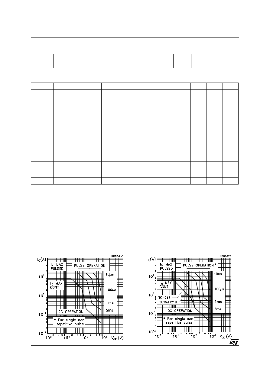
Safe Operating Area (TO-3)
Safe Operating Areas (TO-218/ISOWATT218)
BU208A / BU508A / BU508AFI
2/8
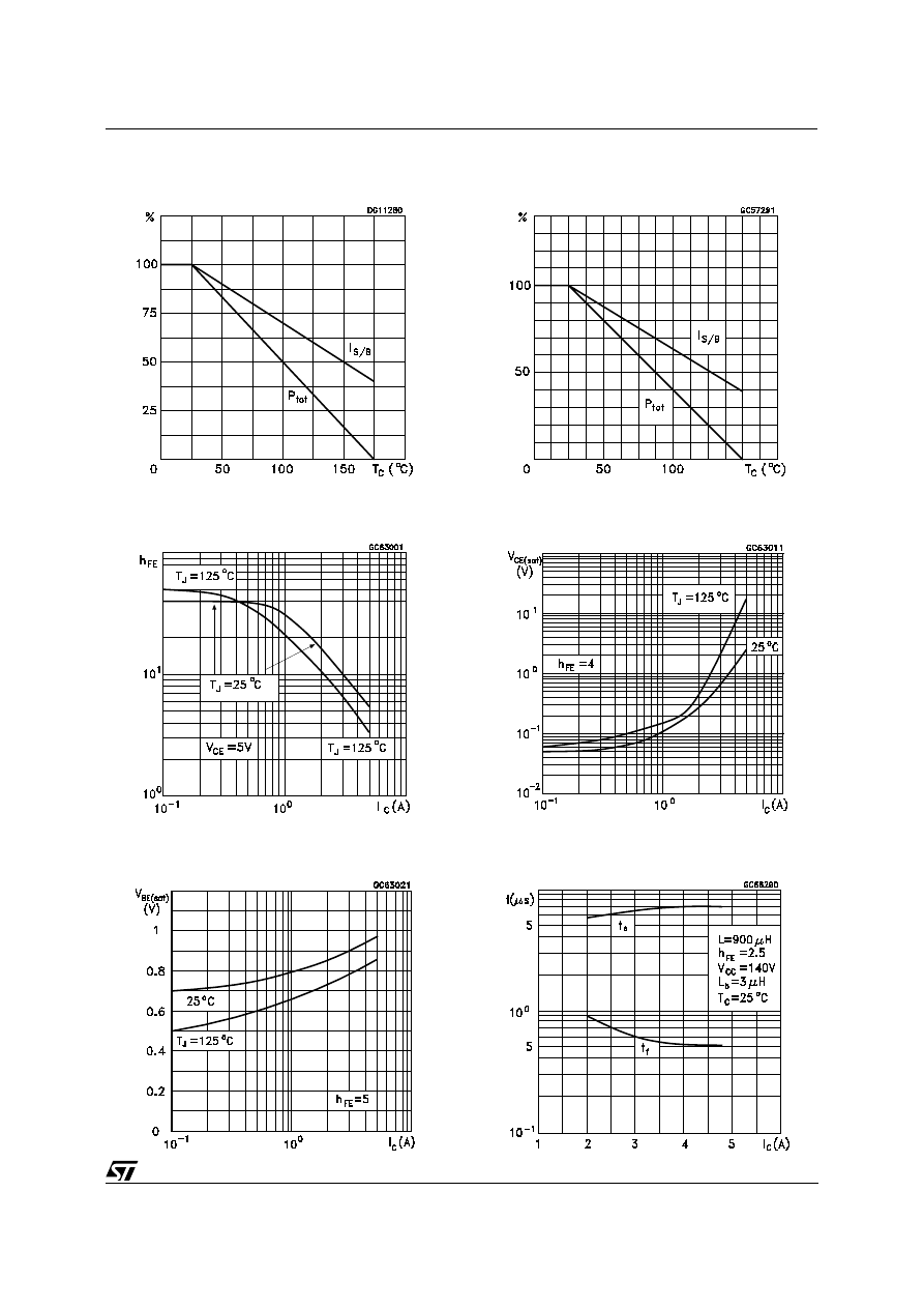
Derating Curves (TO-3)
DC Current Gain
Base Emitter Saturation Voltage
Derating Curves (TO-218/ISOWATT218)
Collector Emitter Saturation Voltage
Switching Time Inductive Load
BU208A / BU508A / BU508AFI
3/8
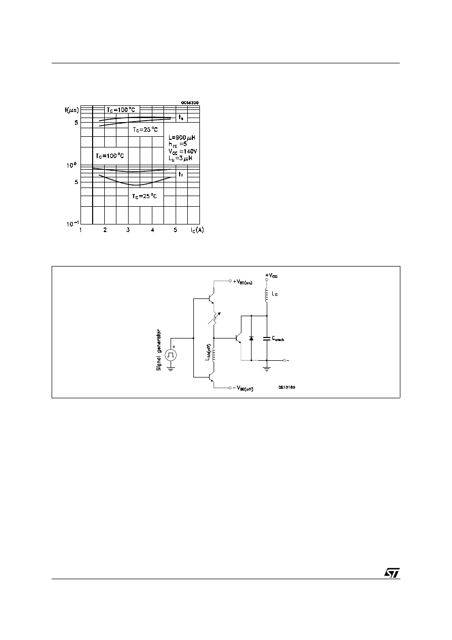
Figure 1: Inductive Load Switching Test Circuit.
Switching Time Inductive Load
BU208A / BU508A / BU508AFI
4/8
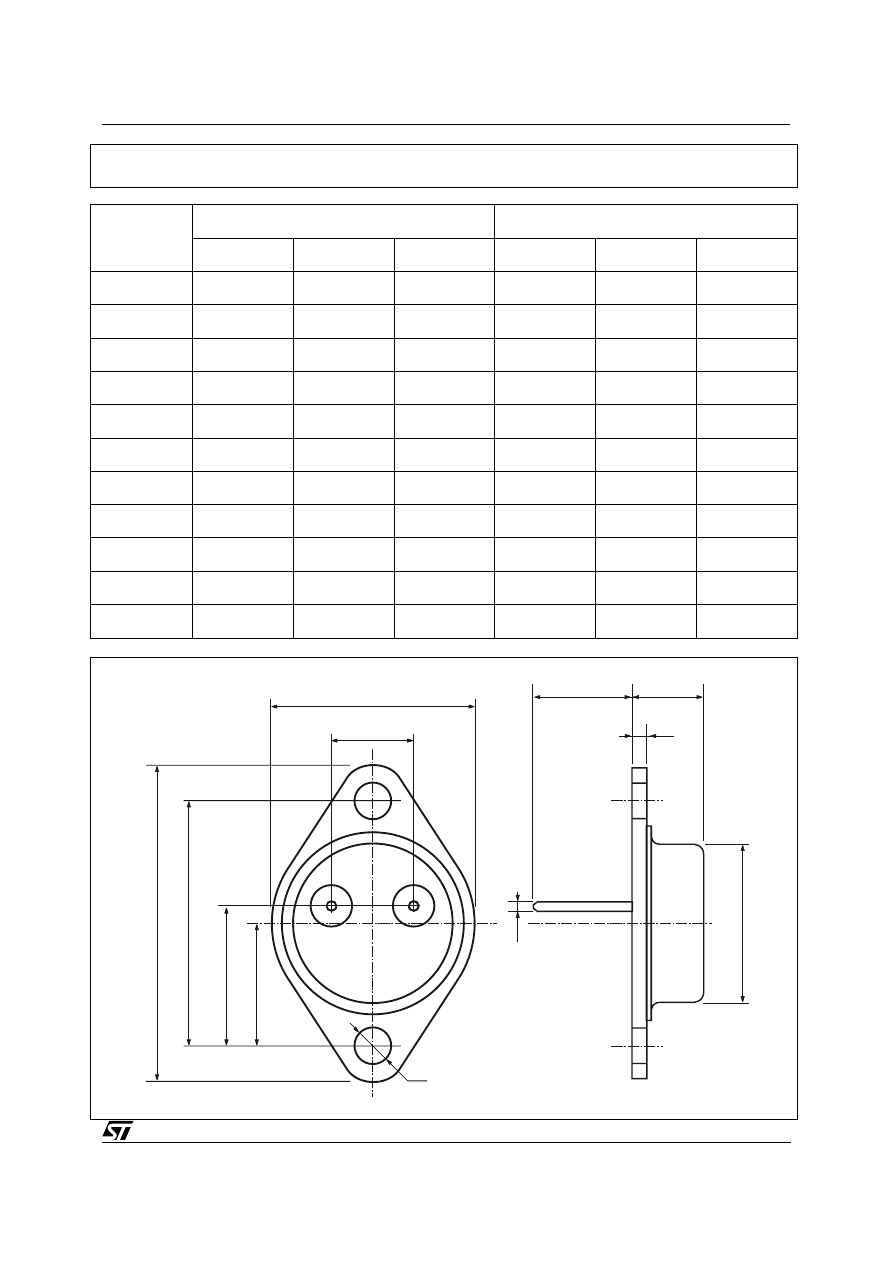
DIM.
mm
inch
MIN.
TYP.
MAX.
MIN.
TYP.
MAX.
A
11.00
13.10
0.433
0.516
B
0.97
1.15
0.038
0.045
C
1.50
1.65
0.059
0.065
D
8.32
8.92
0.327
0.351
E
19.00
20.00
0.748
0.787
G
10.70
11.10
0.421
0.437
N
16.50
17.20
0.649
0.677
P
25.00
26.00
0.984
1.023
R
4.00
4.09
0.157
0.161
U
38.50
39.30
1.515
1.547
V
30.00
30.30
1.187
1.193
E
B
R
C
D
A
P
G
N
V
U
O
P003F
TO-3 MECHANICAL DATA
BU208A / BU508A / BU508AFI
5/8
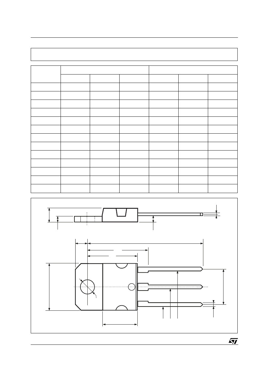
DIM.
mm
inch
MIN.
TYP.
MAX.
MIN.
TYP.
MAX.
A
4.7
4.9
0.185
0.193
C
1.17
1.37
0.046
0.054
D
2.5
0.098
E
0.5
0.78
0.019
0.030
F
1.1
1.3
0.043
0.051
G
10.8
11.1
0.425
0.437
H
14.7
15.2
0.578
0.598
L2
-
16.2 -
0.637
L3
18
0.708
L5
3.95
4.15
0.155
0.163
L6
31
1.220
R
-
12.2
-
0.480
à 4
4.1
0.157
0.161
R
A
C
D
E
H
F
G
L6
¯
L3
L2
L5
1 2 3
TO-218 (SOT-93) MECHANICAL DATA
P025A
BU208A / BU508A / BU508AFI
6/8
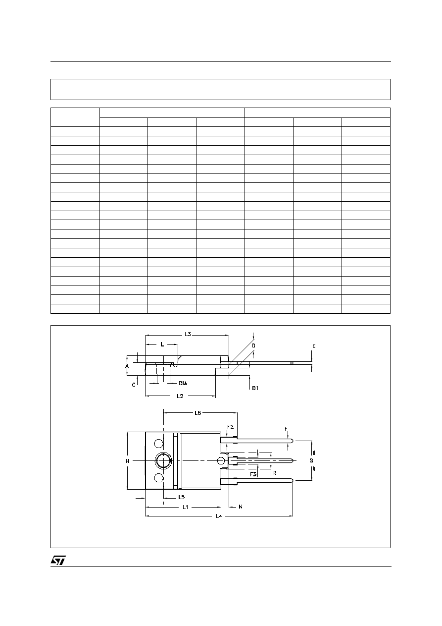
DIM.
mm
inch
MIN.
TYP.
MAX.
MIN.
TYP.
MAX.
A
5.35
5.65
0.211
0.222
C
3.30
3.80
0.130
0.150
D
2.90
3.10
0.114
0.122
D1
1.88
2.08
0.074
0.082
E
0.75
0.95
0.030
0.037
F
1.05
1.25
0.041
0.049
F2
1.50
1.70
0.059
0.067
F3
1.90
2.10
0.075
0.083
G
10.80
11.20
0.425
0.441
H
15.80
16.20
0.622
0.638
L
9
0.354
L1
20.80
21.20
0.819
0.835
L2
19.10
19.90
0.752
0.783
L3
22.80
23.60
0.898
0.929
L4
40.50
42.50
1.594
1.673
L5
4.85
5.25
0.191
0.207
L6
20.25
20.75
0.797
0.817
N
2.1
2.3
0.083
0.091
R
4.6
0.181
DIA
3.5
3.7
0.138
0.146
P025C/A
ISOWATT218 MECHANICAL DATA
- Weight : 4.9 g (typ.)
- Maximum Torque (applied to mounting flange) Recommended: 0.8 Nm; Maximum: 1 Nm
- The side of the dissipator must be flat within 80
µ
m
BU208A / BU508A / BU508AFI
7/8

Information furnished is believed to be accurate and reliable. However, STMicroelectronics assumes no responsibility for the consequences
of use of such information nor for any infringement of patents or other rights of third parties which may result from its use. No license is
granted by implication or otherwise under any patent or patent rights of STMicroelectronics. Specification mentioned in this publication are
subject to change without notice. This publication supersedes and replaces all information previously supplied. STMicroelectronics products
are not authorized for use as critical components in life support devices or systems without express written approval of STMicroelectronics.
The ST logo is a trademark of STMicroelectronics
© 2002 STMicroelectronics - Printed in Italy - All Rights Reserved
STMicroelectronics GROUP OF COMPANIES
Australia - Brazil - Canada - China - Finland - France - Germany - Hong Kong - India - Israel - Italy - Japan - Malaysia - Malta - Morocco -
Singapore - Spain - Sweden - Switzerland - United Kingdom - United States.
http://www.st.com
BU208A / BU508A / BU508AFI
8/8