| Secciones |
|---|
| Foros Electrónica |
|
|
| Boletines de correo |
 |

CD4017BC,CD4017BM,CD4022BC,CD4022BM
CD4017BM CD4017BC Decade Counter/Divider with 10 Decoded Outputs CD4022BM
CD4022BC Divide-by-8 Counter/Divider with 8 Decoded Outputs
Literature Number: SNOS357A
TL/F/5950
CD4017BM/CD4017BC
Decade
Counter/Divider
with
10
Decoded
Outputs
CD4022BM/CD4022BC
Divide-by-8
Counter/Divider
with
8
Decoded
Outputs
March 1988
CD4017BM/CD4017BC Decade Counter/Divider
with 10 Decoded Outputs
CD4022BM/CD4022BC Divide-by-8 Counter/Divider
with 8 Decoded Outputs
General Description
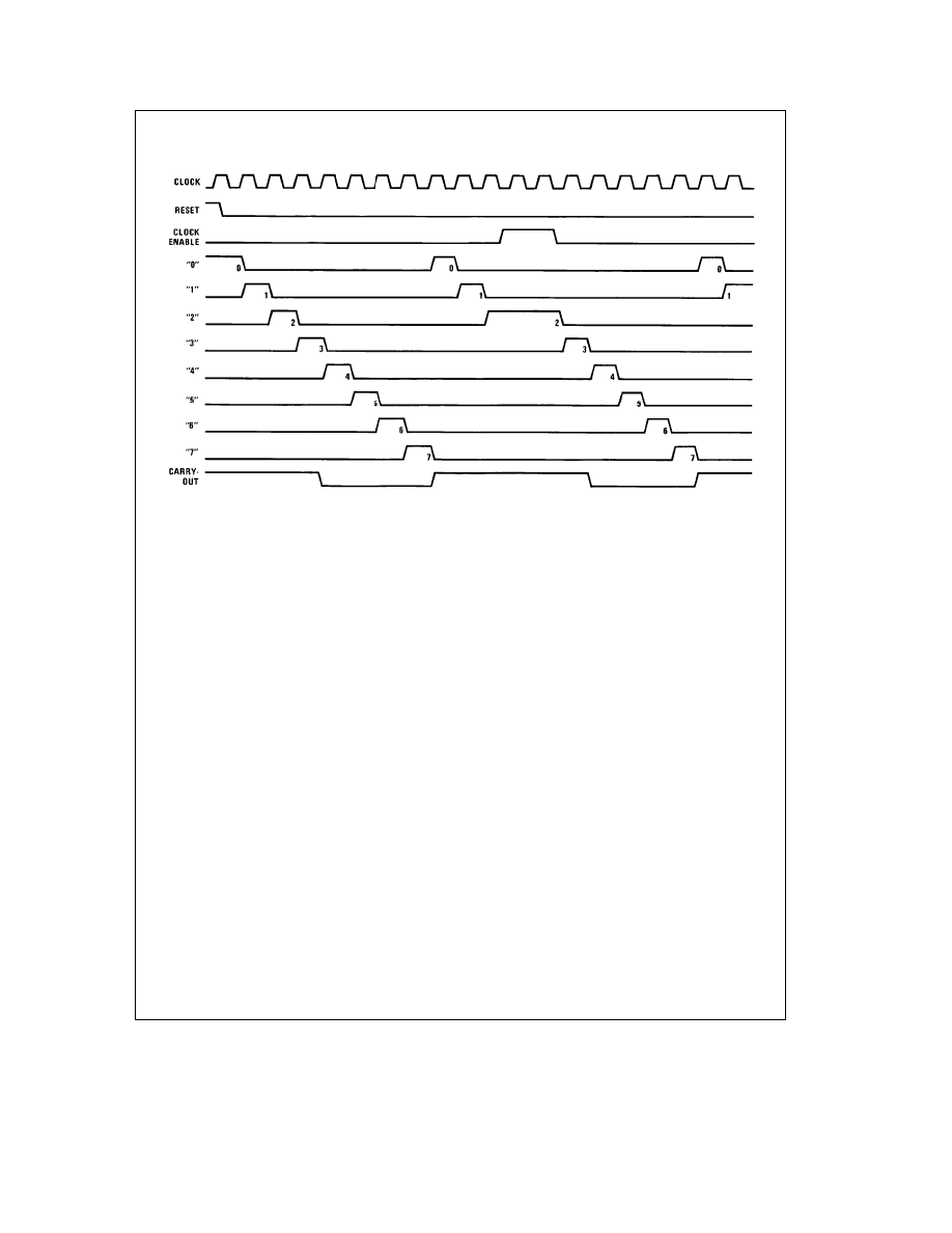
The CD4017BM/CD4017BC is a 5-stage divide-by-10 John-
son counter with 10 decoded outputs and a carry out bit.
The CD4022BM/CD4022BC is a 4-stage divide-by-8 John-
son counter with 8 decoded outputs and a carry-out bit.
These counters are cleared to their zero count by a logical
1 on their reset line. These counters are advanced on the
positive edge of the clock signal when the clock enable sig-
nal is in the logical 0 state.
The configuration of the CD4017BM/CD4017BC and
CD4022BM/CD4022BC permits medium speed operation
and assures a hazard free counting sequence. The 10/8
decoded outputs are normally in the logical 0 state and go
to the logical 1 state only at their respective time slot.
Each decoded output remains high for 1 full clock cycle.
The carry-out signal completes a full cycle for every 10/8
clock input cycles and is used as a ripple carry signal to any
succeeding stages.
Features
Y
Wide supply voltage range
3.0V to 15V
Y
High noise immunity
0.45 V
DD
(typ.)
Y
Low power
Fan out of 2 driving 74L
TTL compatibility
or 1 driving 74LS
Y
Medium speed operation
5.0 MHz (typ.)
with 10V V
DD
Y
Low power
10 mW (typ.)
Y
Fully static operation
Applications
Y
Automotive
Y
Instrumentation
Y
Medical electronics
Y
Alarm systems
Y
Industrial electronics
Y
Remote metering
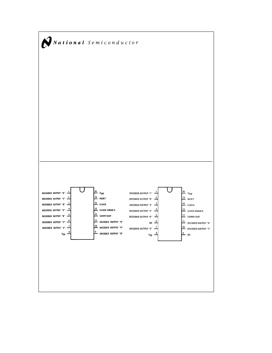
Connection Diagrams
CD4017B
Dual-In-Line Package
TL/F/5950 - 1
Top View
CD4022B
Dual-In-Line Package
TL/F/5950 - 2
Top View
Order Number CD4017B or CD4022B
C1995 National Semiconductor Corporation
RRD-B30M105/Printed in U. S. A.
Obsolete
Absolute Maximum Ratings
(Notes 1 & 2)
If Military/Aerospace specified devices are required,
please contact the National Semiconductor Sales
Office/Distributors for availability and specifications.
DC Supply Voltage (V
DD
)
b
0.5 V
DC
to
a
18 V
DC
Input Voltage (V
IN
)
b
0.5 V
DC
to V
DD
a
0.5 V
DC
Storage Temperature (T
S
)
b
65
§
C to
a
150
§
C
Power Dissipation (P
D
)
Dual-In-Line
700 mW
Small Outline
500 mW
Lead Temperature (T
L
)
(Soldering, 10 seconds)
260
§
C
Recommended Operating
Conditions
(Note 2)
DC Supply Voltage (V
DD
)
a
3 V
DC
to
a
15 V
DC
Input Voltage (V
IN
)
0 to V
DD
V
DC
Operating Temperature Range (T
A
)
CD4017BM, CD4022BM
b
55
§
C to
a
125
§
C
CD4017BC, CD4022BC
b
40
§
C to
a
85
§
C
DC Electrical Characteristics
CD4017BM, CD4022BM (Note 2)
Symbol
Parameter
Conditions
b
55
§
C
a
25
§
a
125
§
C
Units
Min
Max
Min
Typ
Max
Min
Max
I
DD
Quiescent Device
V
DD
e
5V, V
IN
e
V
DD
or V
SS
5
0.3
5
150
m
A
Current
V
DD
e
10V, V
IN
e
V
DD
or V
SS
10
0.5
10
300
m
A
V
DD
e
15V, V
IN
e
V
DD
or V
SS
20
1.0
20
600
m
A
V
OL
Low Level
l
I
O
l
k
1.0 mA
Output Voltage
V
DD
e
5V
0.05
0
0.05
0.05
V
V
DD
e
10V
0.05
0
0.05
0.05
V
V
DD
e
15V
0.05
0
0.05
0.05
V
V
OH
High Level
l
I
O
l
k
1.0 mA
Output Voltage
V
DD
e
5V
4.95
4.95
5
4.95
V
V
DD
e
10V
9.95
9.95
10
9.95
V
V
DD
e
15V
14.95
14.95
15
14.95
V
V
IL
Low Level
l
I
O
l
k
1.0 mA
Input Voltage
V
DD
e
5V, V
O
e
0.5V or 4.5V
1.5
1.5
1.5
V
V
DD
e
10V, V
O
e
1.0V or 9.0V
3.0
3.0
3.0
V
V
DD
e
15V, V
O
e
1.5V or 13.5V
4.0
4.0
4.0
V
V
IH
High Level
l
I
O
l
k
1.0 mA
Input Voltage
V
DD
e
5V, V
O
e
0.5V or 4.5V
3.5
3.5
3.5
V
V
DD
e
10V, V
O
e
1.0V or 9.0V
7.0
7.0
7.0
V
V
DD
e
15V, V
O
e
1.5V or 13.5V
11.0
11.0
11.0
V
I
OL
Low Level Output
V
DD
e
5V, V
O
e
0.4V
0.64
0.51
0.88
0.36
mA
Current (Note 3)
V
DD
e
10V, V
O
e
0.5V
1.6
1.3
2.25
0.9
mA
V
DD
e
15V, V
O
e
1.5V
4.2
3.4
8.8
2.4
mA
I
OH
High Level Output
V
DD
e
5V, V
O
e
4.6V
b
0.25
b
0.2
b
0.36
b
0.14
mA
Current (Note 3)
V
DD
e
10V, V
O
e
9.5V
b
0.62
b
0.5
b
0.9
b
0.35
mA
V
DD
e
15V, V
O
e
13.5V
b
1.8
b
1.5
b
3.5
b
1.1
mA
I
IN
Input Current
V
DD
e
15V, V
IN
e
0V
b
0.1
b
10
b
5
b
0.1
b
1.0
m
A
V
DD
e
15V, V
IN
e
15V
0.1
10
b
5
0.1
1.0
m
A
DC Electrical Characteristics
CD4017BC, CD4022BC (Note 2)
Symbol
Parameter
Conditions
b
40
§
C
a
25
§
a
85
§
C
Units
Min
Max
Min
Typ
Max
Min
Max
I
DD
Quiescent Device
V
DD
e
5V
20
0.5
20
150
m
A
Current
V
DD
e
10V
40
1.0
40
300
m
A
V
DD
e
15V
80
5.0
80
600
m
A
V
OL
Low Level
l
I
O
l
k
1.0 mA
Output Voltage
V
DD
e
5V
0.05
0
0.05
0.05
V
V
DD
e
10V
0.05
0
0.05
0.05
V
V
DD
e
15V
0.05
0
0.05
0.05
V
V
OH
High Level
l
I
O
l
k
1.0 mA
Output Voltage
V
DD
e
5V
4.95
4.95
5
4.95
V
V
DD
e
10V
9.95
9.95
10
9.95
V
V
DD
e
15V
14.95
14.95
15
14.95
V
Note 1:
Absolute Maximum Ratings are those values beyond which the safety of the device cannot be guaranteed, they are not meant to imply that the devices
should be operated at these limits. The table of Recommended Operating Conditions and Electrical Characteristics provides conditions for actual device
operation.
Note 2:
V
SS
e
0V unless otherwise specified.
Note 3:
I
OL
and I
OH
are tested one output at a time.
2
Obsolete
DC Electrical Characteristics
CD4017BC, CD4022BC (Note 2) (Continued)
Symbol
Parameter
Conditions
b
40
§
C
a
25
§
a
85
§
C
Units
Min
Max
Min
Typ
Max
Min
Max
V
IL
Low Level
l
I
O
l
k
1.0 mA
Input Voltage
V
DD
e
5V, V
O
e
0.5V or 4.5V
1.5
1.5
1.5
V
V
DD
e
10V, V
O
e
1.0V or 9.0V
3.0
3.0
3.0
V
V
DD
e
15V, V
O
e
1.5V or 13.5V
4.0
4.0
4.0
V
V
IH
High Level
l
I
O
l
k
1.0 mA
Input Voltage
V
DD
e
5V, V
O
e
0.5V or 4.5V
3.5
3.5
3.5
V
V
DD
e
10V, V
O
e
1.0V or 9.0V
7.0
7.0
7.0
V
V
DD
e
15V, V
O
e
1.5V or 13.5V
11.0
11.0
11.0
V
I
OL
Low Level Output
V
DD
e
5V, V
O
e
0.4V
0.52
0.44
0.88
0.36
mA
Current (Note 3)
V
DD
e
10V, V
O
e
0.5V
1.3
1.1
2.25
0.9
mA
V
DD
e
15V, V
O
e
1.5V
3.6
3.0
8.8
2.4
mA
I
OH
High Level Output
V
DD
e
5V, V
O
e
4.6V
b
0.2
b
0.16
b
0.36
b
0.12
mA
Current (Note 3)
V
DD
e
10V, V
O
e
9.5V
b
0.5
b
0.4
b
0.9
b
0.3
mA
V
DD
e
15V, V
O
e
13.5V
b
1.4
b
1.2
b
3.5
b
1.0
mA
I
IN
Input Current
V
DD
e
15V, V
IN
e
0V
b
0.3
b
10
b
5
b
0.3
b
1.0
m
A
V
DD
e
15V, V
IN
e
15V
0.3
10
b
5
0.3
1.0
m
A
Note 1:
Absolute Maximum Ratings are those values beyond which the safety of the device cannot be guaranteed, they are not meant to imply that the devices
should be operated at these limits. The table of Recommended Operating Conditions and Electrical Characteristics provides condtions for actual device
operation.
Note 2:
V
SS
e
0V unless otherwise specified.
Note 3:
I
OL
and I
OH
are tested one output at a time.
AC Electrical Characteristics
*
T
A
e
25
§
C, C
L
e
50 pF, R
L
e
200k, t
rCL
and t
fCL
e
20 ns, unless otherwise specified
Symbol
Parameter
Conditions
Min
Typ
Max
Units
CLOCK OPERATION
t
PHL,
t
PLH
Propagation Delay Time
Carry Out Line
V
DD
e
5V
415
800
ns
V
DD
e
10V
160
320
ns
V
DD
e
15V
130
250
ns
Carry Out Line
V
DD
e
5V
240
480
ns
V
DD
e
10V
C
L
e
15 pF
85
170
ns
V
DD
e
15V
(
70
140
ns
Decode Out Lines
V
DD
e
5V
500
1000
ns
V
DD
e
10V
200
400
ns
V
DD
e
15V
160
320
ns
t
TLH
, t
THL
Transition Time Carry Out
and Decode Out Lines
t
TLH
V
DD
e
5V
200
360
ns
V
DD
e
10V
100
180
ns
V
DD
e
15V
80
130
ns
t
THL
V
DD
e
5V
100
200
ns
V
DD
e
10V
50
100
ns
V
DD
e
15V
40
80
ns
f
CL
Maximum Clock Frequency
V
DD
e
5V
Measured with
1.0
2
MHz
V
DD
e
10V
Respect to Carry
2.5
5
MHz
V
DD
e
15V
(
Output Line
3.0
6
MHz
t
WL
, t
WH
Minimum Clock
V
DD
e
5V
125
250
ns
Pulse Width
V
DD
e
10V
45
90
ns
V
DD
e
15V
35
70
ns
t
rCL
, t
fCL
Clock Rise and
V
DD
e
5V
20
m
s
Fall Time
V
DD
e
10V
15
m
s
V
DD
e
15V
5
m
s
t
SU
Minimum Clock Inhibit
V
DD
e
5V
120
240
ns
Data Setup Time
V
DD
e
10V
40
80
ns
V
DD
e
15V
32
65
ns
C
IN
Average Input Capacitance
5
7.5
pF
3
Obsolete
AC Electrical Characteristics
*
T
A
e
25
§
C, C
L
e
50 pF, R
L
e
200k, t
rCL
and t
fCL
e
20 ns, unless otherwise specified
Symbol
Parameter
Conditions
Min
Typ
Max
Units
RESET OPERATION
t
PHL, tPLH
Propagation Delay Time
Carry Out Line
V
DD
e
5V
415
800
ns
V
DD
e
10V
160
320
ns
V
DD
e
15V
130
250
ns
Carry Out Line
V
DD
e
5V
240
480
ns
V
DD
e
10V
C
L
e
15 pF
85
170
ns
V
DD
e
15V
(
70
140
ns
Decode Out Lines
V
DD
e
5V
500
1000
ns
V
DD
e
10V
200
400
ns
V
DD
e
15V
160
320
ns
t
W
Minimum Reset
V
DD
e
5V
200
400
ns
Pulse Width
V
DD
e
10V
70
140
ns
V
DD
e
15V
55
110
ns
t
REM
Minimum Reset
V
DD
e
5V
75
150
ns
Removal Time
V
DD
e
10V
30
60
ns
V
DD
e
15V
25
50
ns
*AC Parameters are guaranteed by DC correlated testing.
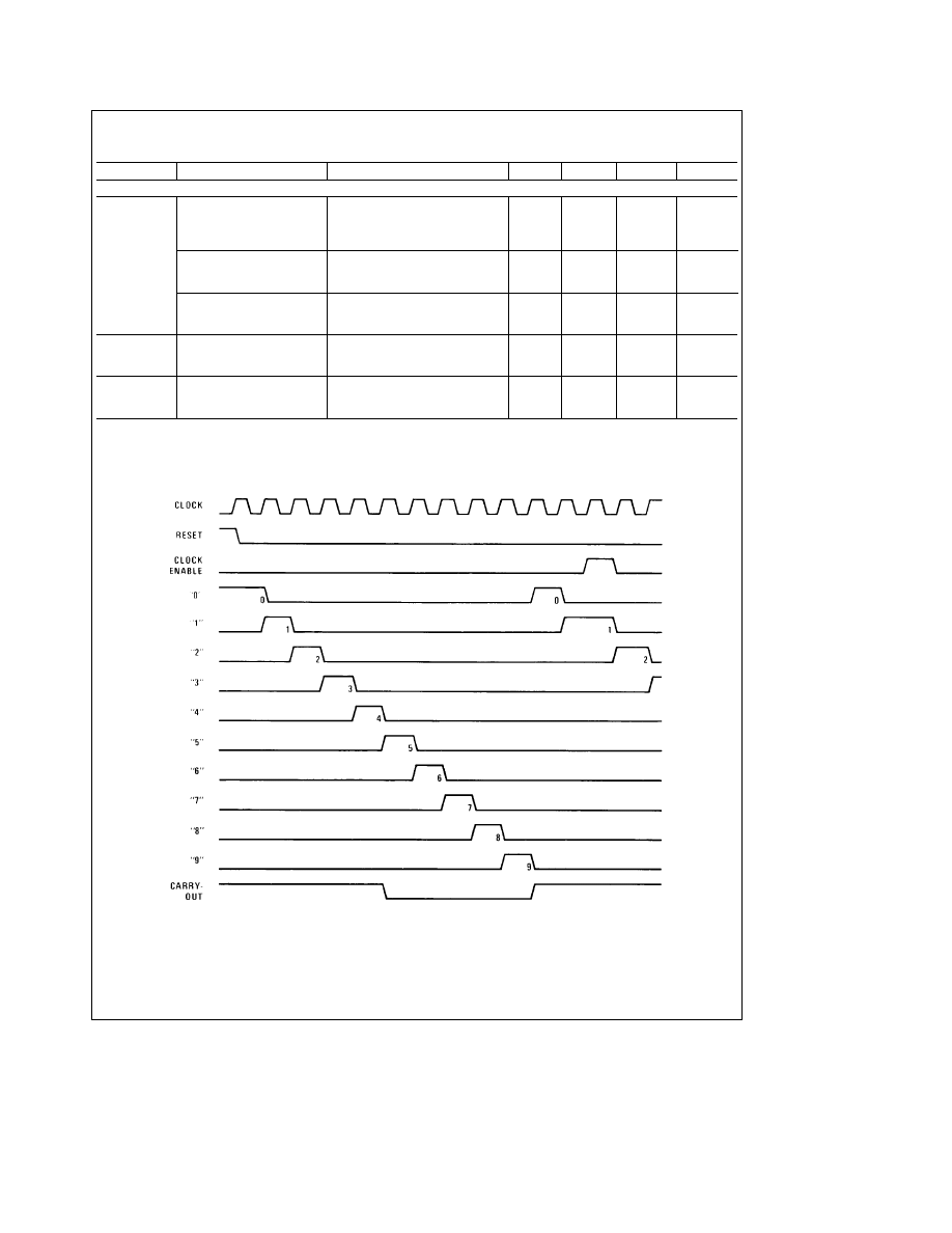
Timing Diagrams
CD4017B
TL/F/5950 - 3
4
Obsolete
Timing Diagrams
(Continued)
CD4022B
TL/F/5950 - 4
5
Obsolete
Logic Diagrams
CD4017B
Terminal No. 8
e
GND
TL/F/5950 - 5
Terminal No. 16
e
V
DD
CD4022B
Terminal No. 16
e
V
DD
TL/F/5950 - 6
Terminal No. 8
e
GND
6
Obsolete
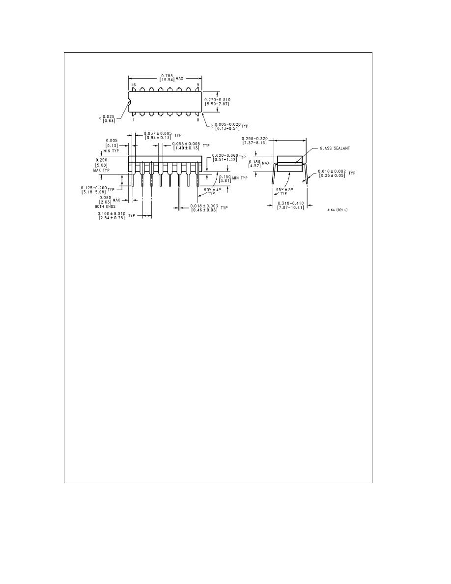
Physical Dimensions
inches (millimeters)
Ceramic Dual-In-Line Package (J)
Order Number CD4017BMJ, CD4017BCJ, CD4022BMJ, CD4022BCJ
NS Package Number J16A
7
Obsolete
CD4017BM/CD4017BC
Decade
Counter/Divider
with
10
Decoded
Outputs
CD4022BM/CD4022BC
Divide-by-8
Counter/Divider
with
8
Decoded
Outputs
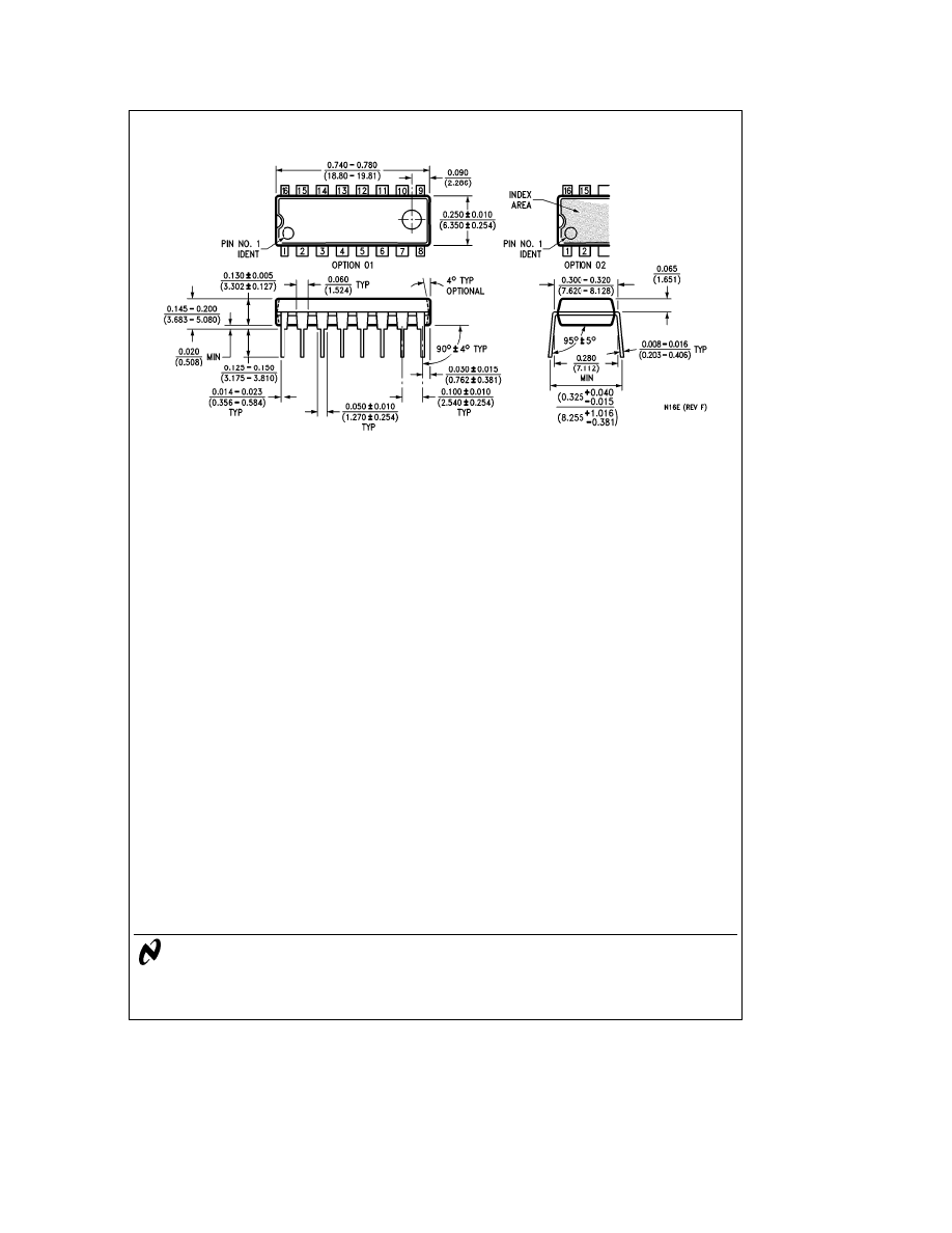
Physical Dimensions
inches (millimeters) (Continued)
Molded Dual-In-Line Package (N)
Order Number CD4017BMN, CD4017BCN, CD4022BMN, CD4022BCN
NS Package Number N16E
LIFE SUPPORT POLICY
NATIONALS PRODUCTS ARE NOT AUTHORIZED FOR USE AS CRITICAL COMPONENTS IN LIFE SUPPORT
DEVICES OR SYSTEMS WITHOUT THE EXPRESS WRITTEN APPROVAL OF THE PRESIDENT OF NATIONAL
SEMICONDUCTOR CORPORATION. As used herein:
1. Life support devices or systems are devices or
2. A critical component is any component of a life
systems which, (a) are intended for surgical implant
support device or system whose failure to perform can
into the body, or (b) support or sustain life, and whose
be reasonably expected to cause the failure of the life
failure to perform, when properly used in accordance
support device or system, or to affect its safety or
with instructions for use provided in the labeling, can
effectiveness.
be reasonably expected to result in a significant injury
to the user.
National Semiconductor
National Semiconductor
National Semiconductor
National Semiconductor
Corporation
Europe
Hong Kong Ltd.
Japan Ltd.
1111 West Bardin Road
Fax: (a49) 0-180-530 85 86
13th Floor, Straight Block,
Tel: 81-043-299-2309
Arlington, TX 76017
Email: cnjwge
@
tevm2.nsc.com
Ocean Centre, 5 Canton Rd.
Fax: 81-043-299-2408
Tel: 1(800) 272-9959
Deutsch Tel: (a49) 0-180-530 85 85
Tsimshatsui, Kowloon
Fax: 1(800) 737-7018
English
Tel: (a49) 0-180-532 78 32
Hong Kong
Fran
3ais Tel: (a49) 0-180-532 93 58
Tel: (852) 2737-1600
Italiano
Tel: (a49) 0-180-534 16 80
Fax: (852) 2736-9960
National does not assume any responsibility for use of any circuitry described, no circuit patent licenses are implied and National reserves the right at any time without notice to change said circuitry and specifications.
Obsolete

IMPORTANT NOTICE
Texas Instruments Incorporated and its subsidiaries (TI) reserve the right to make corrections, modifications, enhancements, improvements,
and other changes to its products and services at any time and to discontinue any product or service without notice. Customers should
obtain the latest relevant information before placing orders and should verify that such information is current and complete. All products are
sold subject to TI
s terms and conditions of sale supplied at the time of order acknowledgment.
TI warrants performance of its hardware products to the specifications applicable at the time of sale in accordance with TI
s standard
warranty. Testing and other quality control techniques are used to the extent TI deems necessary to support this warranty. Except where
mandated by government requirements, testing of all parameters of each product is not necessarily performed.
TI assumes no liability for applications assistance or customer product design. Customers are responsible for their products and
applications using TI components. To minimize the risks associated with customer products and applications, customers should provide
adequate design and operating safeguards.
TI does not warrant or represent that any license, either express or implied, is granted under any TI patent right, copyright, mask work right,
or other TI intellectual property right relating to any combination, machine, or process in which TI products or services are used. Information
published by TI regarding third-party products or services does not constitute a license from TI to use such products or services or a
warranty or endorsement thereof. Use of such information may require a license from a third party under the patents or other intellectual
property of the third party, or a license from TI under the patents or other intellectual property of TI.
Reproduction of TI information in TI data books or data sheets is permissible only if reproduction is without alteration and is accompanied
by all associated warranties, conditions, limitations, and notices. Reproduction of this information with alteration is an unfair and deceptive
business practice. TI is not responsible or liable for such altered documentation. Information of third parties may be subject to additional
restrictions.
Resale of TI products or services with statements different from or beyond the parameters stated by TI for that product or service voids all
express and any implied warranties for the associated TI product or service and is an unfair and deceptive business practice. TI is not
responsible or liable for any such statements.
TI products are not authorized for use in safety-critical applications (such as life support) where a failure of the TI product would reasonably
be expected to cause severe personal injury or death, unless officers of the parties have executed an agreement specifically governing
such use. Buyers represent that they have all necessary expertise in the safety and regulatory ramifications of their applications, and
acknowledge and agree that they are solely responsible for all legal, regulatory and safety-related requirements concerning their products
and any use of TI products in such safety-critical applications, notwithstanding any applications-related information or support that may be
provided by TI. Further, Buyers must fully indemnify TI and its representatives against any damages arising out of the use of TI products in
such safety-critical applications.
TI products are neither designed nor intended for use in military/aerospace applications or environments unless the TI products are
specifically designated by TI as military-grade or
"
enhanced plastic.
"
Only products designated by TI as military-grade meet military
specifications. Buyers acknowledge and agree that any such use of TI products which TI has not designated as military-grade is solely at
the Buyer
'
s risk, and that they are solely responsible for compliance with all legal and regulatory requirements in connection with such use.
TI products are neither designed nor intended for use in automotive applications or environments unless the specific TI products are
designated by TI as compliant with ISO/TS 16949 requirements. Buyers acknowledge and agree that, if they use any non-designated
products in automotive applications, TI will not be responsible for any failure to meet such requirements.
Following are URLs where you can obtain information on other Texas Instruments products and application solutions:
Products
Applications
Audio
Communications and Telecom
Amplifiers
Computers and Peripherals
Data Converters
Consumer Electronics
DLP
®
Products
Energy and Lighting
DSP
Industrial
Clocks and Timers
Medical
Interface
Security
Logic
Space, Avionics and Defense
Power Mgmt
Transportation and Automotive
Microcontrollers
Video and Imaging
RFID
OMAP Mobile Processors
Wireless Connectivity
TI E2E Community Home Page
Mailing Address: Texas Instruments, Post Office Box 655303, Dallas, Texas 75265
Copyright
©
2011, Texas Instruments Incorporated

