| Secciones |
|---|
| Foros Electrónica |
|
|
| Boletines de correo |
 |
© 2002 Fairchild Semiconductor Corporation
DS005969
www.fairchildsemi.com
October 1987
Revised March 2002
CD404
7BC
Low Power
Monost
a
ble/
Ast
a
ble
Mult
ivi
b
rat
o
r
CD4047BC
Low Power Monostable/Astable Multivibrator
General Description
The CD4047B is capable of operating in either the
monostable or astable mode. It requires an external capac-
itor (between pins 1 and 3) and an external resistor
(between pins 2 and 3) to determine the output pulse width
in the monostable mode, and the output frequency in the
astable mode.
Astable operation is enabled by a high level on the astable
input or low level on the astable input. The output fre-
quency (at 50% duty cycle) at Q and Q outputs is deter-
mined by the timing components. A frequency twice that of
Q is available at the Oscillator Output; a 50% duty cycle is
not guaranteed.
Monostable operation is obtained when the device is trig-
gered by LOW-to-HIGH transition at
+
trigger input or
HIGH-to-LOW transition at
-
trigger input. The device can
be retriggered by applying a simultaneous LOW-to-HIGH
transition to both the
+
trigger and retrigger inputs.
A high level on Reset input resets the outputs Q to LOW, Q
to HIGH.
Features
Wide supply voltage range:
3.0V to 15V
High noise immunity:
0.45 V
DD
(typ.)
Low power TTL compatibility:
Fan out of 2 driving 74L
or 1 driving 74LS
Special Features
Low power consumption: special CMOS oscillator
configuration
Monostable (one-shot) or astable (free-running)
operation
True and complemented buffered outputs
Only one external R and C required
Monostable Multivibrator
Features
Positive- or negative-edge trigger
Output pulse width independent of trigger pulse duration
Retriggerable option for pulse width expansion
Long pulse widths possible using small RC components
by means of external counter provision
Fast recovery time essentially independent of pulse
width
Pulse-width accuracy maintained at duty cycles
approaching 100%
Astable Multivibrator Features
Free-running or gatable operating modes
50% duty cycle
Oscillator output available
Good astable frequency stability
typical
=
±
2%
+
0.03%/
°
C @ 100 kHz
frequency
=
±
0.5%
+
0.015%/
°
C @ 10 kHz
deviation (circuits trimmed to frequency V
DD
=
10V
±
10%)
Applications
Frequency discriminators
Timing circuits
Time-delay applications
Envelope detection
Frequency multiplication
Frequency division
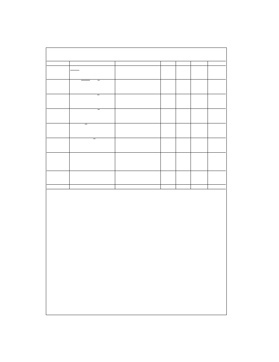
Ordering Code:
Devices also available in Tape and Reel. Specify by appending the suffix letter X to the ordering code.
Order Number
Package Number
Package Description
CD4047BCM
M14A
14-Lead Small Outline Integrated Circuit (SOIC), JEDEC MS-012, 0.150" Narrow
CD4047BCN
N14A
14-Lead Plastic Dual-In-Line Package (PDIP), JEDEC MS-001, 0.300" Wide
www.fairchildsemi.com
2
C
D
40
47BC
Connection Diagram
Pin Assignments for SOIC and DIP
Top View
Function Table
Note 1: External resistor between terminals 2 and 3. External capacitor between terminals 1 and 3.
Typical Implementation of External Countdown Option
t
EXT
=
(N
-
1) t
A
+
(t
M
+
t
A
/2)
FIGURE 1.
Terminal Connections
Output Pulse
Typical Output
Function
To V
DD
To V
SS
Input Pulse
From
Period or
To
Pulse Width
Astable Multivibrator
Free-Running
4, 5, 6, 14
7, 8, 9, 12
10, 11, 13
t
A
(10, 11)
=
4.40 RC
True Gating
4, 6, 14
7, 8, 9, 12
5
10, 11, 13
t
A
(13)
=
2.20 RC
Complement Gating
6, 14
5, 7, 8, 9, 12
4
10, 11, 13
Monostable Multivibrator
Positive-Edge Trigger
4, 14
5, 6, 7, 9, 12
8
10, 11
Negative-Edge Trigger
4, 8, 14
5, 7, 9, 12
6
10, 11
t
M
(10, 11)
=
2.48 RC
Retriggerable
4, 14
5, 6, 7, 9
8, 12
10, 11
External Countdown (Note 1)
14
5, 6, 7, 8, 9, 12
Figure 1
Figure 1
Figure 1
3
www.fairchildsemi.com
CD404
7BC
Block Diagram
Logic Diagram
*Special input protection circuit to permit larger input-voltage swings.
www.fairchildsemi.com
4
C
D
40
47BC
Absolute Maximum Ratings
(Note 2)
(Note 3)
Recommended Operating
Conditions
(Note 3)
Note 2: Absolute Maximum Ratings are those values beyond which the
safety of the device cannot be guaranteed. They are not meant to imply
that the devices should be operated at these limits. The table of Recom-
mended Operating Conditions and Electrical Characteristics provides
conditions for actual device operation.
Note 3: V
SS
=
0V unless otherwise specified.
DC Electrical Characteristics
(Note 3)
Note 4: I
OH
and I
OL
are tested one output at a time.
DC Supply Voltage (V
DD
)
-
0.5V to
+
18V
DC
Input Voltage (V
IN
)
-
0.5V to V
DD
+
0.5V
DC
Storage Temperature Range (T
S
)
-
65
°
C to
+
150
°
C
Power Dissipation (P
D
)
Dual-In-Line
700 mW
Small Outline
500 mW
Lead Temperature (T
L
)
(Soldering, 10 seconds)
260
°
C
DC Supply Voltage (V
DD
)
3V to 15V
DC
Input Voltage (V
IN
)
0 to V
DD
V
DC
Operating Temperature Range (T
A
)
-
55
°
C to
+
125
°
C
Symbol
Parameter
Conditions
-
55
°
C
25
°
C
125
°
C
Units
Min
Max
Min
Typ
Max
Min
Max
I
DD
Quiescent Device Current
V
DD
=
5V
5
5
150
µ
A
V
DD
=
10V
10
10
300
V
DD
=
15V
20
20
600
V
OL
LOW Level Output Voltage
|I
O
|
<
1
µ
A
V
DD
=
5V
0.05
0
0.05
0.05
V
V
DD
=
10V
0.05
0
0.05
0.05
V
DD
=
15V
0.05
0
0.05
0.05
V
OH
HIGH Level Output Voltage
|I
O
|
<
1
µ
A
V
DD
=
5V
4.95
4.95
5
4.95
V
V
DD
=
10V
9.95
9.95
10
9.95
V
DD
=
15V
14.95
14.95
15
14.95
V
IL
LOW Level Input Voltage
V
DD
=
5V, V
O
=
0.5V or 4.5V
1.5
2.25
1.5
1.5
V
V
DD
=
10V, V
O
=
1V or 9V
3.0
4.5
3.0
3.0
V
DD
=
15V, V
O
=
1.5V or 13.5V
4.0
6.75
4.0
4.0
V
IH
HIGH Level Input Voltage
V
DD
=
5V, V
O
=
0.5V or 4.5V
3.5
3.5
2.75
3.5
V
V
DD
=
10V, V
O
=
1V or 9V
7.0
7.0
5.5
7.0
V
DD
=
15V, V
O
=
1.5V or 13.5V
11.0
11.0
8.25
11.0
I
OL
LOW Level Output Current
V
DD
=
5V, V
O
=
0.4V
0.64
0.51
0.88
0.36
mA
(Note 4)
V
DD
=
10V, V
O
=
0.5V
1.6
1.3
2.25
0.9
V
DD
=
15V, V
O
=
1.5V
4.2
3.4
8.8
2.4
I
OH
HIGH Level Output Current
V
DD
=
5V, V
O
=
4.6V
-
0.64
-
0.51
-
0.88
-
0.36
mA
(Note 4)
V
DD
=
10V, V
O
=
9.5V
-
1.6
-
1.3
-
2.25
-
0.9
V
DD
=
15V, V
O
=
13.5V
-
4.2
-
3.4
-
8.8
-
2.4
I
IN
Input Current
V
DD
=
15V, V
IN
=
0V
-
0.1
-
10
-
5
-
0.1
-
1.0
µ
A
V
DD
=
15V, V
IN
=
15V
0.1
10
-
5
0.1
1.0
5
www.fairchildsemi.com
CD404
7BC
AC Electrical Characteristics
(Note 5)
T
A
=
25
°
C, C
L
=
50 pF, R
L
=
200k, input t
r
=
t
f
=
20 ns, unless otherwise specified.
Note 5: AC Parameters are guaranteed by DC correlated testing.
Symbol
Parameter
Conditions
Min
Typ
Max
Units
t
PHL
, t
PLH
Propagation Delay Time Astable,
V
DD
=
5V
200
400
ns
Astable to Osc Out
V
DD
=
10V
100
200
V
DD
=
15V
80
160
t
PHL
, t
PLH
Astable, Astable to Q, Q
V
DD
=
5V
550
900
ns
V
DD
=
10V
250
500
V
DD
=
15V
200
400
t
PHL
, t
PLH
+
Trigger,
-
Trigger to Q
V
DD
=
5V
700
1200
ns
V
DD
=
10V
300
600
V
DD
=
15V
240
480
t
PHL
, t
PLH
+
Trigger, Retrigger to Q
V
DD
=
5V
300
600
ns
V
DD
=
10V
175
300
V
DD
=
15V
150
250
t
PHL
, t
PLH
Reset to Q, Q
V
DD
=
5V
300
600
ns
V
DD
=
10V
125
250
V
DD
=
15V
100
200
t
THL
, t
TLH
Transition Time Q, Q, Osc Out
V
DD
=
5V
100
200
ns
V
DD
=
10V
50
100
V
DD
=
15V
40
80
t
WL
, t
WH
Minimum Input Pulse Duration
Any Input
V
DD
=
5V
500
1000
ns
V
DD
=
10V
200
400
V
DD
=
15V
160
320
t
RCL
, t
FCL
+
Trigger, Retrigger, Rise and
V
DD
=
5V
15
µ
s
Fall Time
V
DD
=
10V
5
V
DD
=
15V
5
C
IN
Average Input Capacitance
Any Input
5
7.5
pF
www.fairchildsemi.com
6
C
D
40
47BC
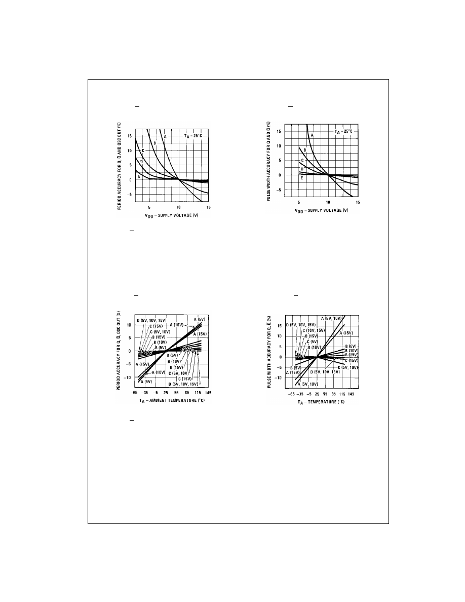
Typical Performance Characteristics
Typical Q, Q, Osc Out Period Accuracy vs
Supply Voltage (Astable Mode Operation)
Typical Q, Q, Pulse Width Accuracy vs
Supply Voltage Monostable Mode Operation
Typical Q, Q and Osc Out Period Accuracy
vs Temperature Astable Mode Operation
Typical Q and Q Pulse Width Accuracy vs
Temperature Monostable Mode Operation
f
Q
, Q
R
C
A
1000 kHz
22k
10 pF
B
100 kHz
22k
100 pF
C
10 kHz
220k
100 pF
D
1 kHz
220k
1000 pF
E
100 Hz
2.2M
1000 pF
t
M
R
C
A
2
µ
s
22k
10 pF
B
7
µ
s
22k
100 pF
C
60
µ
s
220k
100 pF
D
550
µ
s
220k
1000 pF
E
5.5 ms
2.2M
1000 pF
f
Q
, Q
R
C
A
1000 kHz
22k
10 pF
B
100 kHz
22k
100 pF
C
10 kHz
220k
100 pF
D
1 kHz
220k
1000 pF
t
M
R
C
A
2
µ
s
22k
10 pF
B
7
µ
s
22k
100 pF
C
60
µ
s
220k
100 pF
D
550
µ
s
220k
1000 pF
Note:
Minimum Value of R:
10 K
Ω¦
Maximum Value of R: 1 Meg
Ω¦
Minimum Value of C for Astable Mode: 100 pF
Minimum Value of C for Monostable Mode: 1000 pF
7
www.fairchildsemi.com
CD404
7BC
Typical Performance Characteristics
(Continued)
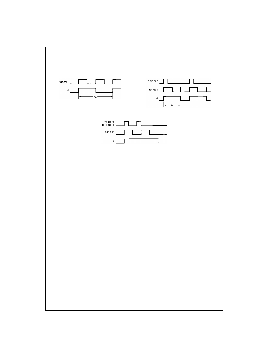
Timing Diagrams
Astable Mode
Monostable Mode
Retrigger Mode
www.fairchildsemi.com
8
C
D
40
47BC
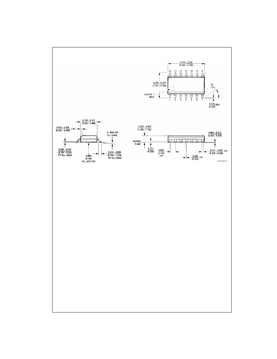
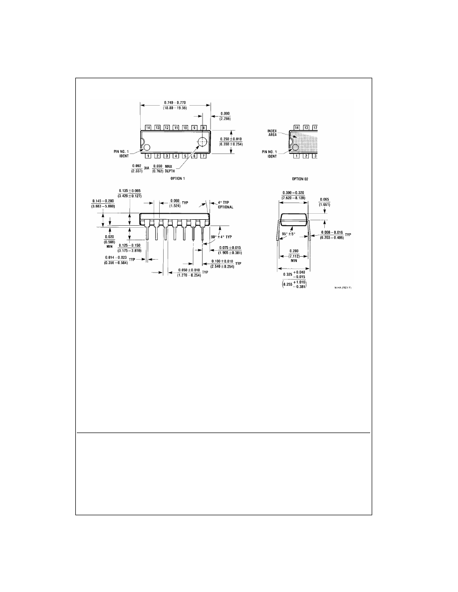
Physical Dimensions
inches (millimeters) unless otherwise noted
14-Lead Small Outline Integrated Circuit (SOIC), JEDEC MS-012, 0.150" Narrow
Package Number M14A
9
www.fairchildsemi.com
CD404
7BC
Low Power
Monost
a
ble/
Ast
a
ble
Mult
ivi
b
rat
o
r
Physical Dimensions
inches (millimeters) unless otherwise noted (Continued)
14-Lead Plastic Dual-In-Line Package (PDIP), JEDEC MS-001, 0.300" Wide
Package Number N14A
Fairchild does not assume any responsibility for use of any circuitry described, no circuit patent licenses are implied and
Fairchild reserves the right at any time without notice to change said circuitry and specifications.
LIFE SUPPORT POLICY
FAIRCHILDS PRODUCTS ARE NOT AUTHORIZED FOR USE AS CRITICAL COMPONENTS IN LIFE SUPPORT
DEVICES OR SYSTEMS WITHOUT THE EXPRESS WRITTEN APPROVAL OF THE PRESIDENT OF FAIRCHILD
SEMICONDUCTOR CORPORATION. As used herein:
1. Life support devices or systems are devices or systems
which, (a) are intended for surgical implant into the
body, or (b) support or sustain life, and (c) whose failure
to perform when properly used in accordance with
instructions for use provided in the labeling, can be rea-
sonably expected to result in a significant injury to the
user.
2. A critical component in any component of a life support
device or system whose failure to perform can be rea-
sonably expected to cause the failure of the life support
device or system, or to affect its safety or effectiveness.
www.fairchildsemi.com

