| Secciones |
|---|
| Foros Electrónica |
|
|
| Boletines de correo |
 |
1
CAUTION: These devices are sensitive to electrostatic discharge; follow proper IC Handling Procedures.
Copyright
©
2004, Texas Instruments Incorporated
Data sheet acquired from Harris Semiconductor
SCHS046I
CD4049UB, CD4050B
CMOS Hex Buffer/Converters
The CD4049UB and CD4050B devices are inverting and
non-inverting hex buffers, respectively, and feature logic-
level conversion using only one supply voltage (V
CC
). The
input-signal high level (V
IH
) can exceed the V
CC
supply
voltage when these devices are used for logic-level
conversions. These devices are intended for use as CMOS
to DTL/TTL converters and can drive directly two DTL/TTL
loads. (V
CC
= 5V, V
OL
≤
0.4V, and I
OL
≥
3.3mA.)
The CD4049UB and CD4050B are designated as
replacements for CD4009UB and CD4010B, respectively.
Because the CD4049UB and CD4050B require only one
power supply, they are preferred over the CD4009UB and
CD4010B and should be used in place of the CD4009UB
and CD4010B in all inverter, current driver, or logic-level
conversion applications. In these applications the
CD4049UB and CD4050B are pin compatible with the
CD4009UB and CD4010B respectively, and can be
substituted for these devices in existing as well as in new
designs. Terminal No. 16 is not connected internally on the
CD4049UB or CD4050B, therefore, connection to this
terminal is of no consequence to circuit operation. For
applications not requiring high sink-current or voltage
conversion, the CD4069UB Hex Inverter is recommended.
Features
CD4049UB Inverting
CD4050B Non-Inverting
High Sink Current for Driving 2 TTL Loads
High-To-Low Level Logic Conversion
100% Tested for Quiescent Current at 20V
Maximum Input Current of 1
µ
A at 18V Over Full Package
Temperature Range; 100nA at 18V and 25
o
C
5V, 10V and 15V Parametric Ratings
Applications
CMOS to DTL/TTL Hex Converter
CMOS Current Sink or Source Driver
CMOS High-To-Low Logic Level Converter
Pinouts
Ordering Information
PART NUMBER
TEMP.
RANGE (
o
C)
PACKAGE
CD4049UBF3A
-55 to 125
16 Ld CERDIP
CD4050BF3A
-55 to 125
16 Ld CERDIP
CD4049UBD
-55 to 125
16 Ld SOIC
CD4049UBDR
-55 to 125
16 Ld SOIC
CD4049UBDT
-55 to 125
16 Ld SOIC
CD4049UBDW
-55 to 125
16 Ld SOIC
CD4049UBDWR
-55 to 125
16 Ld SOIC
CD4049UBE
-55 to 125
16 Ld PDIP
CD4049UBNSR
-55 to 125
16 Ld SOP
CD4049UBPW
-55 to 125
16 Ld TSSOP
CD4049UBPWR
-55 to 125
16 Ld TSSOP
CD4050BD
-55 to 125
16 Ld SOIC
CD4050BDR
-55 to 125
16 Ld SOIC
CD4050UBDT
-55 to 125
16 Ld SOIC
CD4050BDW
-55 to 125
16 Ld SOIC
CD4050BDWR
-55 to 125
16 Ld SOIC
CD4050BE
-55 to 125
16 Ld PDIP
CD4050NSR
-55 to 125
16 Ld SOP
CD4050BPW
-55 to 125
16 Ld TSSOP
CD4050BPWR
-55 to 125
16 Ld TSSOP
NOTE: When ordering, use the entire part number. The suffix R denotes tape
and reel. The suffix T denotes a small-quantity reel of 250.
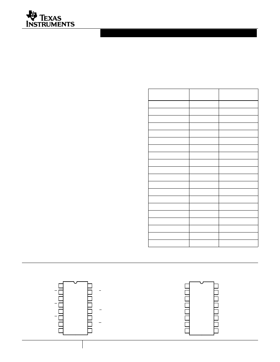
CD4049UB (PDIP, CERDIP, SOIC, SOP, TSSOP)
TOP VIEW
CD4050B (PDIP, CERDIP, SOIC, SOP)
TOP VIEW
14
15
16
9
13
12
11
10
1
2
3
4
5
7
6
8
V
CC
G = A
A
H = B
B
I = C
V
SS
C
NC
F
NC
K = E
E
J = D
D
L = F
14
15
16
9
13
12
11
10
1
2
3
4
5
7
6
8
V
CC
G = A
A
H = B
B
I = C
V
SS
C
NC
F
NC
K = E
E
J = D
D
L = F
August 1998 - Revised May 2004
[ /Title
(CD40
49UB,
CD405
0B)
/Sub-
ject
(CMO
S Hex
Buffer/
Con-
verters)
/Autho
r ()
/Key-
words
(Harris
Semi-
con-
ductor,
CD400
0,
metal
gate,
CMOS
2
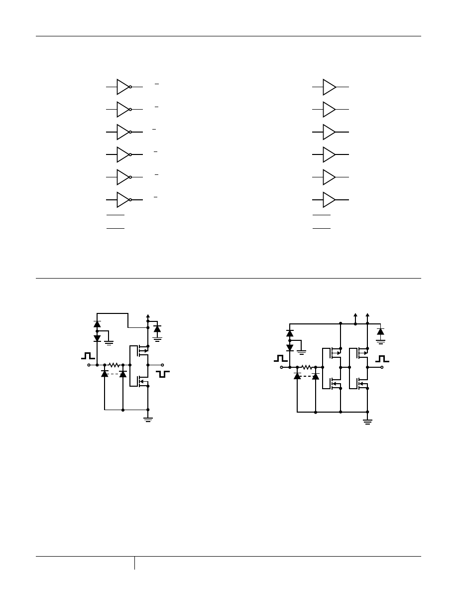
Functional Block Diagrams
CD4049UB
CD4050B
3
2
A
G = A
5
4
B
H = B
7
6
C
I = C
9
10
D
J = D
11
12
E
K = E
14
15
F
L = F
1
8
V
CC
V
SS
NC = 13
NC = 16
3
2
A
G = A
5
4
B
H = B
7
6
C
I = C
9
10
D
J = D
11
12
E
K = E
14
15
F
L = F
1
8
V
CC
V
SS
NC = 13
NC = 16
Schematic Diagrams
FIGURE 1A. SCHEMATIC DIAGRAM OF CD4049UB, 1 OF 6
IDENTICAL UNITS
FIGURE 1B. SCHEMATIC DIAGRAM OF CD4050B, 1 OF 6
IDENTICAL UNITS
V
CC
OUT
V
SS
P
N
R
IN
P
N
R
IN
V
CC
OUT
V
SS
P
N
CD4049UB, CD4050B
3
Absolute Maximum Ratings
Thermal Information
Supply Voltage (V+ to V-). . . . . . . . . . . . . . . . . . . . . . . -0.5V to 20V
DC Input Current, Any One Input. . . . . . . . . . . . . . . . . . . . . .
±
10mA
Operating Conditions
Temperature Range . . . . . . . . . . . . . . . . . . . . . . . . . -55
o
C to 125
o
C
Package Thermal Impedance,
Θ
JA
(see Note1):
E (PDIP) Package . . . . . . . . . . . . . . . . . . . . . . . . . . . . . . 67
o
C/W
D (SOIC) Package . . . . . . . . . . . . . . . . . . . . . . . . . . . . . . 73
o
C/W
DW (SOIC) Package . . . . . . . . . . . . . . . . . . . . . . . . . . . . 57
o
C/W
NS (SOP) Package . . . . . . . . . . . . . . . . . . . . . . . . . . . . . 64
o
C/W
PW (TSSOP) Package . . . . . . . . . . . . . . . . . . . . . . . . . . 108
o
C/W
Maximum Junction Temperature (Plastic Package) . . . . . . . . .150
o
C
Maximum Storage Temperature Range . . . . . . . . . . . 65
o
C to 150
o
C
Maximum Lead Temperature (Soldering 10s) . . . . . . . . . . . . .265
o
C
SOIC - Lead Tips Only
CAUTION: Stresses above those listed in Absolute Maximum Ratings may cause permanent damage to the device. This is a stress only rating and operation of the
device at these or any other conditions above those indicated in the operational sections of this specification is not implied.
NOTE:
1. The package thermal impedance is calculated in accordance with JESD 51-7.
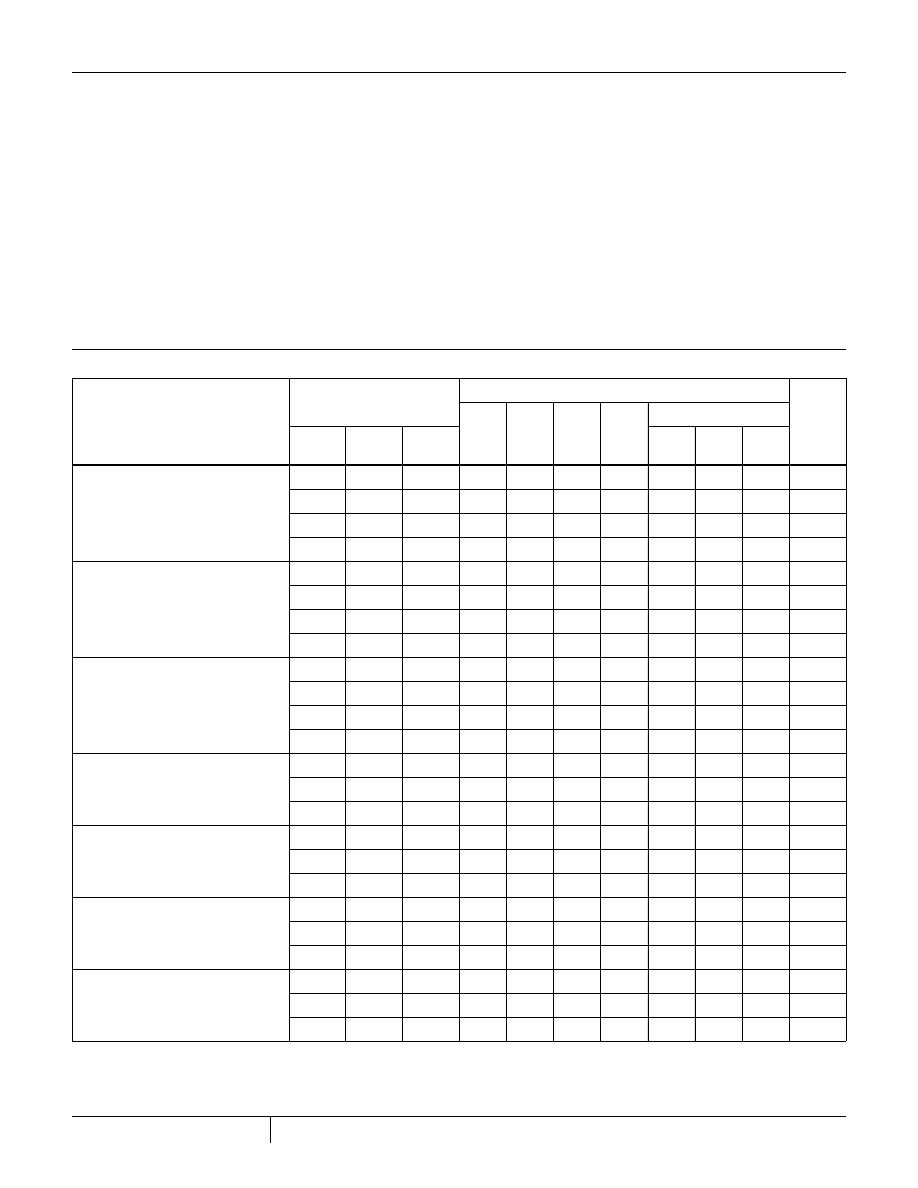
DC Electrical Specifications
PARAMETER
TEST CONDITIONS
LIMITS AT INDICATED TEMPERATURE (
o
C)
UNITS
-55
-40
85
125
25
V
O
(V)
V
IN
(V)
V
CC
(V)
MIN
TYP
MAX
Quiescent Device Current
I
DD
(Max)
-
0,5
5
1
1
30
30
-
0.02
1
µ
A
-
0,10
10
2
2
60
60
-
0.02
2
µ
A
-
0,15
15
4
4
120
120
-
0.02
4
µ
A
-
0,20
20
20
20
600
600
-
0.04
20
µ
A
Output Low (Sink) Current
I
OL
(Min)
0.4
0,5
4.5
3.3
3.1
2.1
1.8
2.6
5.2
-
mA
0.4
0,5
5
4
3.8
2.9
2.4
3.2
6.4
-
mA
0.5
0,10
10
10
9.6
6.6
5.6
8
16
-
mA
1.5
0,15
15
26
25
20
18
24
48
-
mA
Output High (Source) Current
I
OH
(Min)
4.6
0,5
5
-0.81
-0.73
-0.58
-0.48
-0.65
-1.2
-
mA
2.5
0,5
5
-2.6
-2.4
-1.9
-1.55
-2.1
-3.9
-
mA
9.5
0,10
10
-2.0
-1.8
-1.35
-1.18
-1.65
-3.0
-
mA
13.5
0,15
15
-5.2
-4.8
-3.5
-3.1
-4.3
-8.0
-
mA
Out Voltage Low Level
V
OL
(Max)
-
0,5
5
0.05
0.05
0.05
0.05
-
0
0.05
V
-
0,10
10
0.05
0.05
0.05
0.05
-
0
0.05
V
-
0,15
15
0.05
0.05
0.05
0.05
-
0
0.05
V
Output Voltage High Level
V
OH
(Min)
-
0,5
5
4.95
4.95
4.95
4.95
4.95
5
-
V
-
0,10
10
9.95
9.95
9.95
9.95
9.95
10
-
V
-
0,15
15
14.95
14.95
14.95
14.95
14.95
15
-
V
Input Low Voltage, V
IL
(Max)
CD4049UB
4.5
-
5
1
1
1
1
-
-
1
V
9
-
10
2
2
2
2
-
-
2
V
13.5
-
15
2.5
2.5
2.5
2.5
-
-
2.5
V
Input Low Voltage, V
IL
(Max)
CD4050B
0.5
-
5
1.5
1.5
1.5
1.5
-
-
1.5
V
1
-
10
3
3
3
3
-
-
3
V
1.5
-
15
4
4
4
4
-
-
4
V
CD4049UB, CD4050B
4
Input High Voltage, V
IH
Min
CD4049UB
0.5
-
5
4
4
4
4
4
-
-
V
1
-
10
8
8
8
8
8
-
-
V
1.5
-
15
12.5
12.5
12.5
12.5
12.5
-
-
V
Input High Voltage, V
IH
Min
CD4050B
4.5
-
5
3.5
3.5
3.5
3.5
3.5
-
-
V
9
-
10
7
7
7
7
7
-
-
V
13.5
-
15
11
11
11
11
11
-
-
V
Input Current, I
IN
Max
-
0,18
18
±
0.1
±
0.1
±
1
±
1
-
±
10
-5
±
0.1
µ
A
DC Electrical Specifications
(Continued)
PARAMETER
TEST CONDITIONS
LIMITS AT INDICATED TEMPERATURE (
o
C)
UNITS
-55
-40
85
125
25
V
O
(V)
V
IN
(V)
V
CC
(V)
MIN
TYP
MAX
AC Electrical Specifications
T
A
= 25
o
C, Input t
r
, t
f
= 20ns, C
L
= 50pF, R
L
= 200k
Ω¦
PARAMETER
TEST CONDITIONS
LIMITS (ALL PACKAGES)
UNITS
V
IN
V
CC
TYP
MAX
Propagation Delay Time
Low to High, t
PLH
CD4049UB
5
5
60
120
ns
10
10
32
65
ns
10
5
45
90
ns
15
15
25
50
ns
15
5
45
90
ns
Propagation Delay Time
Low to High, t
PLH
CD4050B
5
5
70
140
ns
10
10
40
80
ns
10
5
45
90
ns
15
15
30
60
ns
15
5
40
80
ns
Propagation Delay Time
High to Low, t
PHL
CD4049UB
5
5
32
65
ns
10
10
20
40
ns
10
5
15
30
ns
15
15
15
30
ns
15
5
10
20
ns
Propagation Delay Time
High to Low, t
PHL
CD4050B
5
5
55
110
ns
10
10
22
55
ns
10
5
50
100
ns
15
15
15
30
ns
15
5
50
100
ns
Transition Time, Low to High, t
TLH
5
5
80
160
ns
10
10
40
80
ns
15
15
30
60
ns
Transition Time, High to Low, t
THL
5
5
30
60
ns
10
10
20
40
ns
15
15
15
30
ns
CD4049UB, CD4050B
5
Input Capacitance, C
IN
CD4049UB
-
-
15
22.5
pF
Input Capacitance, C
IN
CD4050B
-
-
5
7.5
pF
AC Electrical Specifications
T
A
= 25
o
C, Input t
r
, t
f
= 20ns, C
L
= 50pF, R
L
= 200k
Ω¦
(Continued)
PARAMETER
TEST CONDITIONS
LIMITS (ALL PACKAGES)
UNITS
V
IN
V
CC
TYP
MAX
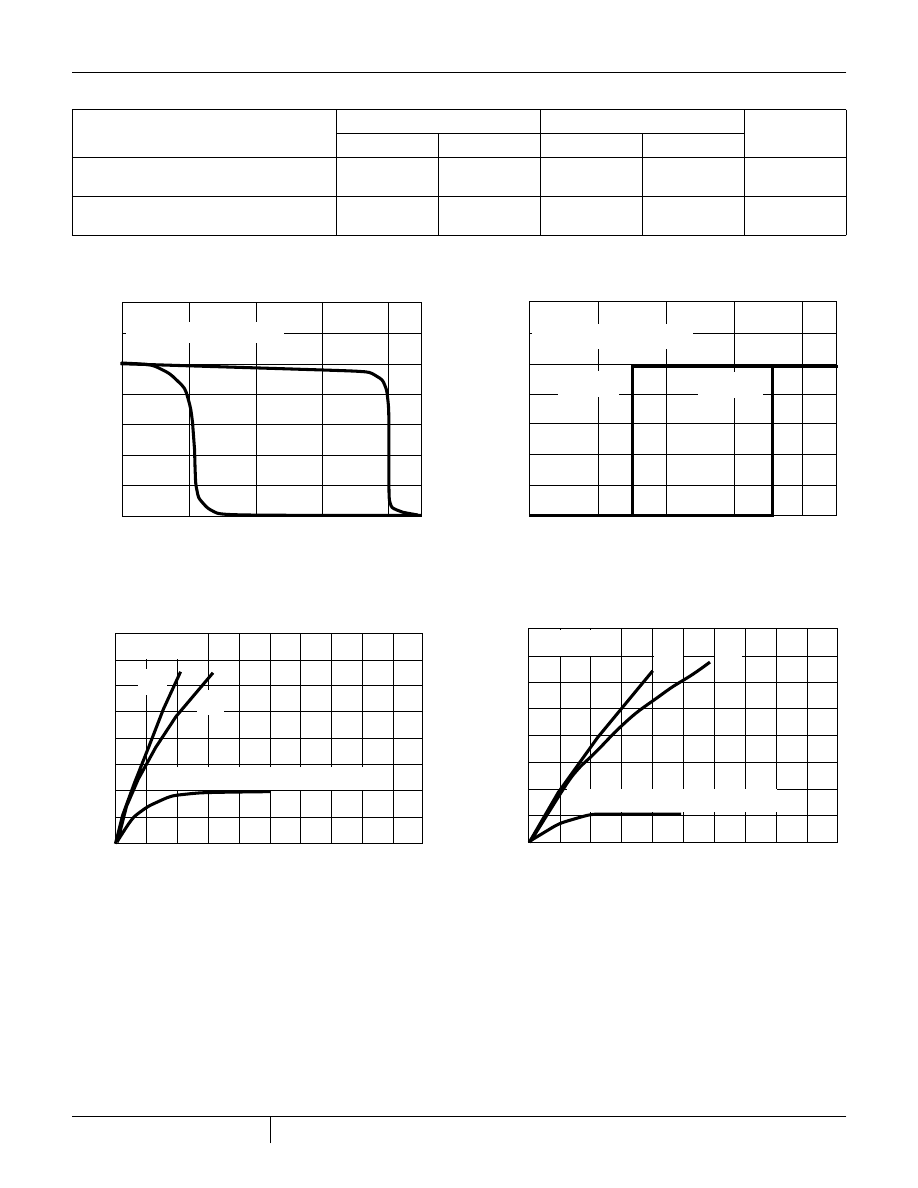
Typical Performance Curves
FIGURE 2. MINIMUM AND MAXIMUM VOLTAGE TRANSFER
CHARACTERISTICS FOR CD4049UB
FIGURE 3. MINIMUM AND MAXIMUM VOLTAGE TRANSFER
CHARACTERISTICS FOR CD4050B
FIGURE 4. TYPICAL OUTPUT LOW (SINK) CURRENT
CHARACTERISTICS
FIGURE 5. MINIMUM OUTPUT LOW (SINK) CURRENT DRAIN
CHARACTERISTICS
5
4
3
2
1
0
1
2
3
4
V
I
, INPUT VOLTAGE (V)
V
O
, OUTPUT V
O
L
T
A
GE (V)
T
A
= 25
o
C
SUPPLY VOLTAGE (V
CC
) = 5V
MAXIMUM
MINIMUM
5
4
3
2
1
0
1
2
3
4
V
I
, INPUT VOLTAGE (V)
V
O
, OUTPUT V
O
L
T
A
GE (V)
T
A
= 25
o
C
SUPPLY VOLTAGE (V
CC
) = 5V
MAXIMUM
MINIMUM
50
40
30
20
10
0
1
2
3
4
V
DS
, DRAIN TO SOURCE VOLTAGE (V)
I
OL
, OUTPUT LO
W (SINK) CURRENT (mA)
T
A
= 25
o
C
GATE TO SOURCE VOLTAGE (V
GS
) = 5V
10V
15V
60
70
5
6
7
8
50
40
30
20
10
0
1
2
3
4
V
DS
, DRAIN TO SOURCE VOLTAGE (V)
I
OL
, OUTPUT LO
W (SINK) CURRENT (mA)
T
A
= 25
o
C
GATE TO SOURCE VOLTAGE (V
GS
) = 5V
10V
15V
60
70
5
6
7
8
CD4049UB, CD4050B
6
FIGURE 6. TYPICAL OUTPUT HIGH (SOURCE) CURRENT
CHARACTERISTICS
FIGURE 7. MINIMUM OUTPUT HIGH (SOURCE) CURRENT
CHARACTERISTICS
FIGURE 8. TYPICAL VOLTAGE TRANSFER CHARACTERISTICS
AS A FUNCTION OF TEMPERATURE FOR CD4049UB
FIGURE 9. TYPICAL VOLTAGE TRANSFER CHARACTERISTICS
AS A FUNCTION OF TEMPERATURE FOR CD4050B
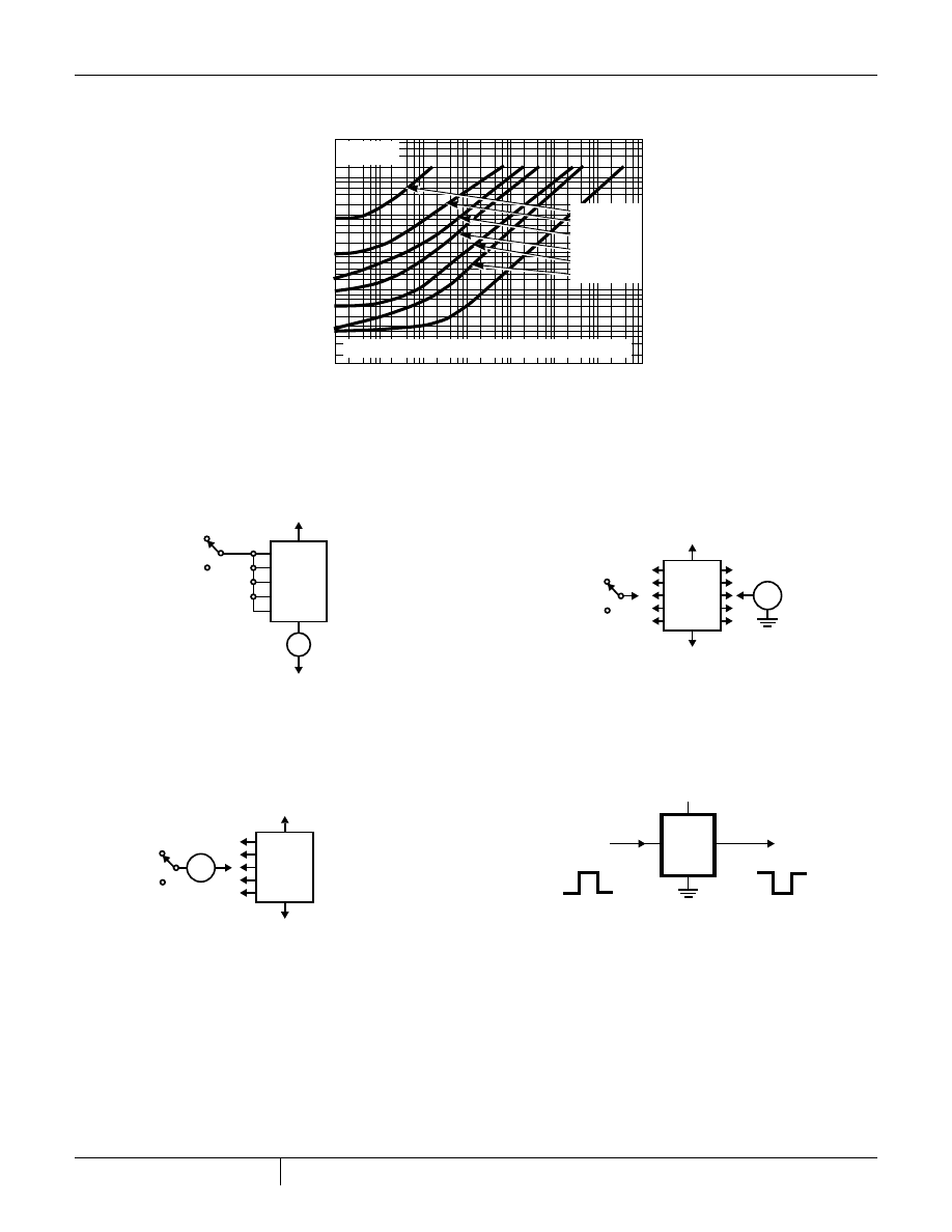
FIGURE 10. TYPICAL POWER DISSIPATION vs FREQUENCY
CHARACTERISTICS
FIGURE 11. TYPICAL POWER DISSIPATION vs INPUT RISE
AND FALL TIMES PER INVERTER FOR CD4049UB
Typical Performance Curves
(Continued)
-5
-10
-15
-20
-25
-30
-35
OUTPUT HIGH (SOURCE)
CURRENT CHARA
CTERISTICS
-15V
-10V
GATE TO SOURCE VOLTAGE
V
GS
= -5V
T
A
= 25
o
C
-8
-7
-6
-5
-4
-3
-2
-1
0
V
DS
, DRAIN TO SOURCE VOLTAGE (V)
-5
-10
-15
-20
-25
-30
-35
OUTPUT HIGH (SOURCE)
CURRENT CHARA
CTERISTICS
-15V
-10V
GATE TO SOURCE VOLTAGE
V
GS
= -5V
T
A
= 25
o
C
-8
-7
-6
-5
-4
-3
-2
-1
0
V
DS
, DRAIN TO SOURCE VOLTAGE (V)
10
6
5
4
3
2
1
V
O
, OUTPUT V
O
L
T
A
GE (V)
-55
o
C
125
o
C
SUPPLY VOLTAGE
V
CC
= 10V
T
A
= -55
o
C
8
7
6
5
4
3
2
1
0
V
I
, INPUT VOLTAGE (V)
9
10
9
8
7
0
125
o
C
V
CC
= 5V
10
6
5
4
3
2
1
V
O
, OUTPUT V
O
L
T
A
GE (V)
-55
o
C
125
o
C
SUPPLY VOLTAGE
V
CC
= 10V
T
A
= -55
o
C
8
7
6
5
4
3
2
1
0
V
I
, INPUT VOLTAGE (V)
9
10
9
8
7
0
125
o
C
V
CC
= 5V
10
5
10
4
10
3
10
2
10
10
10
2
10
3
10
4
10
5
T
A
= 25
o
C
SUPPL
Y V
OL
TA
GE V
CC
= 15V
10V
10V
5V
LOAD CAPACITANCE
C
L
= 50pF
(11pF FIXTURE + 39pF EXT)
(11pF FIXTURE + 4pF EXT)
C
L
= 15pF
PO
WER DISSIP
A
TION PER INVER
TER (
µ
W)
f, INPUT FREQUENCY (kHz)
10
5
10
4
10
3
10
2
10
10
10
2
10
3
10
4
10
5
T
A
= 25
o
C
PO
WER DISSIP
A
TION PER INVER
TER (
µ
W)
t
r
, t
f
, INPUT RISE AND FALL TIME (ns)
SUPPLY VOLTAGE V
CC
= 5V FREQUENCY (f) = 10kHz
15V; 1MHz
15V; 100kHz
10V; 100kHz
15V; 10kHz
10V; 10kHz
15V; 1kHz
10
6
10
7
10
8
CD4049UB, CD4050B
7
FIGURE 12. TYPICAL POWER DISSIPATION vs INPUT RISE
AND FALL TIMES PER INVERTER FOR CD4050B
Typical Performance Curves
(Continued)
10
6
10
4
10
3
10
2
1
10
10
2
10
3
10
4
10
5
T
A
= 25
o
C
PO
WER DISSIP
A
TION PER INVER
TER (
µ
W)
t
r
, t
f
, INPUT RISE AND FALL TIME (ns)
SUPPLY VOLTAGE V
CC
= 5V FREQUENCY (f) = 10kHz
10
6
10
7
10
8
10
10
5
15V; 1MHz
15V; 100kHz
10V; 100kHz
15V; 10kHz
10V; 10kHz
15V; 1kHz
Test Circuits
FIGURE 13. QUIESCENT DEVICE CURRENT TEST CIRCUIT
NOTE: Test any one input with other inputs at V
CC
or V
SS
.
FIGURE 14. INPUT VOLTAGE TEST CIRCUIT
NOTE: Measure inputs sequentially, to both V
CC
and V
SS
connect
all unused inputs to either V
CC
or V
SS
.
FIGURE 15. INPUT CURRENT TEST CIRCUIT
In Terminal - 3, 5, 7, 9, 11, or 14
Out Terminal - 2, 4, 6, 10, 12 or 15
V
CC
Terminal - 1
V
SS
Terminal - 8
FIGURE 16. LOGIC LEVEL CONVERSION APPLICATION
I
DD
V
CC
INPUTS
V
SS
V
CC
V
SS
V
CC
OUTPUTS
INPUTS
V
IH
V
IL
V
SS
DVM
+
-
V
CC
OUTPUTS
INPUTS
V
CC
V
SS
V
SS
I
V
CC
= 5V
OUTPUT
INPUTS
10V = V
IH
0 = V
IL
V
SS
TO DTL/TTL
CMOS 10V LEVEL TO DTL/TTL 5V LEVEL
COS/MOS
IN
0 = V
OL
5V = V
OH
CD4049
CD4049UB, CD4050B
8
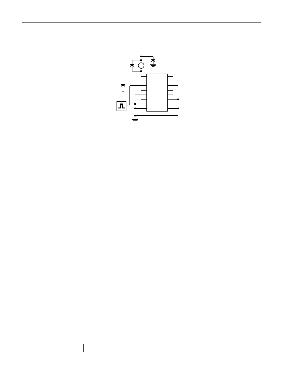
FIGURE 17. DYNAMIC POWER DISSIPATION TEST CIRCUITS
Test Circuits
(Continued)
I
V
DD
500
µ
F
0.1
µ
F
C
L
10kHz,
100kHz, 1MHz
1
2
3
4
5
6
7
8
CD4049UB
16
15
14
13
12
11
10
9
C
L
INCLUDES FIXTURE CAPACITANCE
CD4049UB, CD4050B

9
CD4049UB, CD4050B
PACKAGING INFORMATION
Orderable Device
Status
(1)
Package
Type
Package
Drawing
Pins Package
Qty
Eco Plan
(2)
Lead/Ball Finish
MSL Peak Temp
(3)
CD4049UBD
ACTIVE
SOIC
D
16
40
Green (RoHS &
no Sb/Br)
CU NIPDAU
Level-1-260C-UNLIM
CD4049UBDE4
ACTIVE
SOIC
D
16
40
Green (RoHS &
no Sb/Br)
CU NIPDAU
Level-1-260C-UNLIM
CD4049UBDG4
ACTIVE
SOIC
D
16
40
Green (RoHS &
no Sb/Br)
CU NIPDAU
Level-1-260C-UNLIM
CD4049UBDR
ACTIVE
SOIC
D
16
2500 Green (RoHS &
no Sb/Br)
CU NIPDAU
Level-1-260C-UNLIM
CD4049UBDRE4
ACTIVE
SOIC
D
16
2500 Green (RoHS &
no Sb/Br)
CU NIPDAU
Level-1-260C-UNLIM
CD4049UBDRG4
ACTIVE
SOIC
D
16
2500 Green (RoHS &
no Sb/Br)
CU NIPDAU
Level-1-260C-UNLIM
CD4049UBDT
ACTIVE
SOIC
D
16
250
Green (RoHS &
no Sb/Br)
CU NIPDAU
Level-1-260C-UNLIM
CD4049UBDTE4
ACTIVE
SOIC
D
16
250
Green (RoHS &
no Sb/Br)
CU NIPDAU
Level-1-260C-UNLIM
CD4049UBDTG4
ACTIVE
SOIC
D
16
250
Green (RoHS &
no Sb/Br)
CU NIPDAU
Level-1-260C-UNLIM
CD4049UBDW
ACTIVE
SOIC
DW
16
40
Green (RoHS &
no Sb/Br)
CU NIPDAU
Level-1-260C-UNLIM
CD4049UBDWE4
ACTIVE
SOIC
DW
16
40
Green (RoHS &
no Sb/Br)
CU NIPDAU
Level-1-260C-UNLIM
CD4049UBDWG4
ACTIVE
SOIC
DW
16
40
Green (RoHS &
no Sb/Br)
CU NIPDAU
Level-1-260C-UNLIM
CD4049UBDWR
ACTIVE
SOIC
DW
16
2000 Green (RoHS &
no Sb/Br)
CU NIPDAU
Level-1-260C-UNLIM
CD4049UBDWRE4
ACTIVE
SOIC
DW
16
2000 Green (RoHS &
no Sb/Br)
CU NIPDAU
Level-1-260C-UNLIM
CD4049UBDWRG4
ACTIVE
SOIC
DW
16
2000 Green (RoHS &
no Sb/Br)
CU NIPDAU
Level-1-260C-UNLIM
CD4049UBE
ACTIVE
PDIP
N
16
25
Pb-Free
(RoHS)
CU NIPDAU
N / A for Pkg Type
CD4049UBEE4
ACTIVE
PDIP
N
16
25
Pb-Free
(RoHS)
CU NIPDAU
N / A for Pkg Type
CD4049UBF
ACTIVE
CDIP
J
16
1
TBD
A42
N / A for Pkg Type
CD4049UBF3A
ACTIVE
CDIP
J
16
1
TBD
A42
N / A for Pkg Type
CD4049UBF3AS2283
OBSOLETE
CDIP
J
16
TBD
Call TI
Call TI
CD4049UBF3AS2534
OBSOLETE
CDIP
J
16
TBD
Call TI
Call TI
CD4049UBM
OBSOLETE
SOIC
D
16
TBD
Call TI
Call TI
CD4049UBM96
OBSOLETE
SOIC
D
16
TBD
Call TI
Call TI
CD4049UBNSR
ACTIVE
SO
NS
16
2000 Green (RoHS &
no Sb/Br)
CU NIPDAU
Level-1-260C-UNLIM
CD4049UBNSRE4
ACTIVE
SO
NS
16
2000 Green (RoHS &
no Sb/Br)
CU NIPDAU
Level-1-260C-UNLIM
CD4049UBNSRG4
ACTIVE
SO
NS
16
2000 Green (RoHS &
no Sb/Br)
CU NIPDAU
Level-1-260C-UNLIM
CD4049UBPW
ACTIVE
TSSOP
PW
16
90
Green (RoHS &
no Sb/Br)
CU NIPDAU
Level-1-260C-UNLIM
PACKAGE OPTION ADDENDUM
www.ti.com
15-Oct-2009
Addendum-Page 1
Orderable Device
Status
(1)
Package
Type
Package
Drawing
Pins Package
Qty
Eco Plan
(2)
Lead/Ball Finish
MSL Peak Temp
(3)
CD4049UBPWE4
ACTIVE
TSSOP
PW
16
90
Green (RoHS &
no Sb/Br)
CU NIPDAU
Level-1-260C-UNLIM
CD4049UBPWG4
ACTIVE
TSSOP
PW
16
90
Green (RoHS &
no Sb/Br)
CU NIPDAU
Level-1-260C-UNLIM
CD4049UBPWR
ACTIVE
TSSOP
PW
16
2000 Green (RoHS &
no Sb/Br)
CU NIPDAU
Level-1-260C-UNLIM
CD4049UBPWRE4
ACTIVE
TSSOP
PW
16
2000 Green (RoHS &
no Sb/Br)
CU NIPDAU
Level-1-260C-UNLIM
CD4049UBPWRG4
ACTIVE
TSSOP
PW
16
2000 Green (RoHS &
no Sb/Br)
CU NIPDAU
Level-1-260C-UNLIM
CD4050BD
ACTIVE
SOIC
D
16
40
Green (RoHS &
no Sb/Br)
CU NIPDAU
Level-1-260C-UNLIM
CD4050BDE4
ACTIVE
SOIC
D
16
40
Green (RoHS &
no Sb/Br)
CU NIPDAU
Level-1-260C-UNLIM
CD4050BDG4
ACTIVE
SOIC
D
16
40
Green (RoHS &
no Sb/Br)
CU NIPDAU
Level-1-260C-UNLIM
CD4050BDR
ACTIVE
SOIC
D
16
2500 Green (RoHS &
no Sb/Br)
CU NIPDAU
Level-1-260C-UNLIM
CD4050BDRE4
ACTIVE
SOIC
D
16
2500 Green (RoHS &
no Sb/Br)
CU NIPDAU
Level-1-260C-UNLIM
CD4050BDRG4
ACTIVE
SOIC
D
16
2500 Green (RoHS &
no Sb/Br)
CU NIPDAU
Level-1-260C-UNLIM
CD4050BDT
ACTIVE
SOIC
D
16
250
Green (RoHS &
no Sb/Br)
CU NIPDAU
Level-1-260C-UNLIM
CD4050BDTE4
ACTIVE
SOIC
D
16
250
Green (RoHS &
no Sb/Br)
CU NIPDAU
Level-1-260C-UNLIM
CD4050BDTG4
ACTIVE
SOIC
D
16
250
Green (RoHS &
no Sb/Br)
CU NIPDAU
Level-1-260C-UNLIM
CD4050BDW
ACTIVE
SOIC
DW
16
40
Green (RoHS &
no Sb/Br)
CU NIPDAU
Level-1-260C-UNLIM
CD4050BDWE4
ACTIVE
SOIC
DW
16
40
Green (RoHS &
no Sb/Br)
CU NIPDAU
Level-1-260C-UNLIM
CD4050BDWG4
ACTIVE
SOIC
DW
16
40
Green (RoHS &
no Sb/Br)
CU NIPDAU
Level-1-260C-UNLIM
CD4050BDWR
ACTIVE
SOIC
DW
16
2000 Green (RoHS &
no Sb/Br)
CU NIPDAU
Level-1-260C-UNLIM
CD4050BDWRE4
ACTIVE
SOIC
DW
16
2000 Green (RoHS &
no Sb/Br)
CU NIPDAU
Level-1-260C-UNLIM
CD4050BDWRG4
ACTIVE
SOIC
DW
16
2000 Green (RoHS &
no Sb/Br)
CU NIPDAU
Level-1-260C-UNLIM
CD4050BE
ACTIVE
PDIP
N
16
25
Pb-Free
(RoHS)
CU NIPDAU
N / A for Pkg Type
CD4050BEE4
ACTIVE
PDIP
N
16
25
Pb-Free
(RoHS)
CU NIPDAU
N / A for Pkg Type
CD4050BF
ACTIVE
CDIP
J
16
1
TBD
A42
N / A for Pkg Type
CD4050BF3A
ACTIVE
CDIP
J
16
1
TBD
A42
N / A for Pkg Type
CD4050BF3AS2283
OBSOLETE
CDIP
J
16
TBD
Call TI
Call TI
CD4050BF3AS2534
OBSOLETE
CDIP
J
16
TBD
Call TI
Call TI
CD4050BM
OBSOLETE
SOIC
D
16
TBD
Call TI
Call TI
CD4050BNSR
ACTIVE
SO
NS
16
2000 Green (RoHS &
no Sb/Br)
CU NIPDAU
Level-1-260C-UNLIM
PACKAGE OPTION ADDENDUM
www.ti.com
15-Oct-2009
Addendum-Page 2
Orderable Device
Status
(1)
Package
Type
Package
Drawing
Pins Package
Qty
Eco Plan
(2)
Lead/Ball Finish
MSL Peak Temp
(3)
CD4050BNSRE4
ACTIVE
SO
NS
16
2000 Green (RoHS &
no Sb/Br)
CU NIPDAU
Level-1-260C-UNLIM
CD4050BNSRG4
ACTIVE
SO
NS
16
2000 Green (RoHS &
no Sb/Br)
CU NIPDAU
Level-1-260C-UNLIM
CD4050BPW
ACTIVE
TSSOP
PW
16
90
Green (RoHS &
no Sb/Br)
CU NIPDAU
Level-1-260C-UNLIM
CD4050BPWE4
ACTIVE
TSSOP
PW
16
90
Green (RoHS &
no Sb/Br)
CU NIPDAU
Level-1-260C-UNLIM
CD4050BPWG4
ACTIVE
TSSOP
PW
16
90
Green (RoHS &
no Sb/Br)
CU NIPDAU
Level-1-260C-UNLIM
CD4050BPWR
ACTIVE
TSSOP
PW
16
2000 Green (RoHS &
no Sb/Br)
CU NIPDAU
Level-1-260C-UNLIM
CD4050BPWRE4
ACTIVE
TSSOP
PW
16
2000 Green (RoHS &
no Sb/Br)
CU NIPDAU
Level-1-260C-UNLIM
CD4050BPWRG4
ACTIVE
TSSOP
PW
16
2000 Green (RoHS &
no Sb/Br)
CU NIPDAU
Level-1-260C-UNLIM
JM38510/05553BEA
ACTIVE
CDIP
J
16
1
TBD
A42
N / A for Pkg Type
JM38510/05554BEA
ACTIVE
CDIP
J
16
1
TBD
A42
N / A for Pkg Type
(1)
The marketing status values are defined as follows:
ACTIVE: Product device recommended for new designs.
LIFEBUY: TI has announced that the device will be discontinued, and a lifetime-buy period is in effect.
NRND: Not recommended for new designs. Device is in production to support existing customers, but TI does not recommend using this part in
a new design.
PREVIEW: Device has been announced but is not in production. Samples may or may not be available.
OBSOLETE: TI has discontinued the production of the device.
(2)
Eco Plan - The planned eco-friendly classification: Pb-Free (RoHS), Pb-Free (RoHS Exempt), or Green (RoHS & no Sb/Br) - please check
for the latest availability information and additional product content details.
TBD: The Pb-Free/Green conversion plan has not been defined.
Pb-Free (RoHS): TI's terms "Lead-Free" or "Pb-Free" mean semiconductor products that are compatible with the current RoHS requirements
for all 6 substances, including the requirement that lead not exceed 0.1% by weight in homogeneous materials. Where designed to be soldered
at high temperatures, TI Pb-Free products are suitable for use in specified lead-free processes.
Pb-Free (RoHS Exempt): This component has a RoHS exemption for either 1) lead-based flip-chip solder bumps used between the die and
package, or 2) lead-based die adhesive used between the die and leadframe. The component is otherwise considered Pb-Free (RoHS
compatible) as defined above.
Green (RoHS & no Sb/Br): TI defines "Green" to mean Pb-Free (RoHS compatible), and free of Bromine (Br) and Antimony (Sb) based flame
retardants (Br or Sb do not exceed 0.1% by weight in homogeneous material)
(3)
MSL, Peak Temp. -- The Moisture Sensitivity Level rating according to the JEDEC industry standard classifications, and peak solder
temperature.
Important Information and Disclaimer:The information provided on this page represents TI's knowledge and belief as of the date that it is
provided. TI bases its knowledge and belief on information provided by third parties, and makes no representation or warranty as to the
accuracy of such information. Efforts are underway to better integrate information from third parties. TI has taken and continues to take
reasonable steps to provide representative and accurate information but may not have conducted destructive testing or chemical analysis on
incoming materials and chemicals. TI and TI suppliers consider certain information to be proprietary, and thus CAS numbers and other limited
information may not be available for release.
In no event shall TI's liability arising out of such information exceed the total purchase price of the TI part(s) at issue in this document sold by TI
to Customer on an annual basis.
PACKAGE OPTION ADDENDUM
www.ti.com
15-Oct-2009
Addendum-Page 3
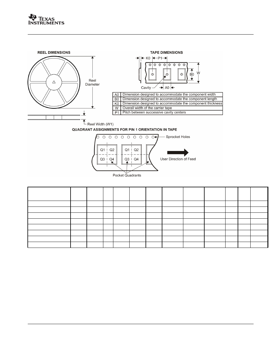
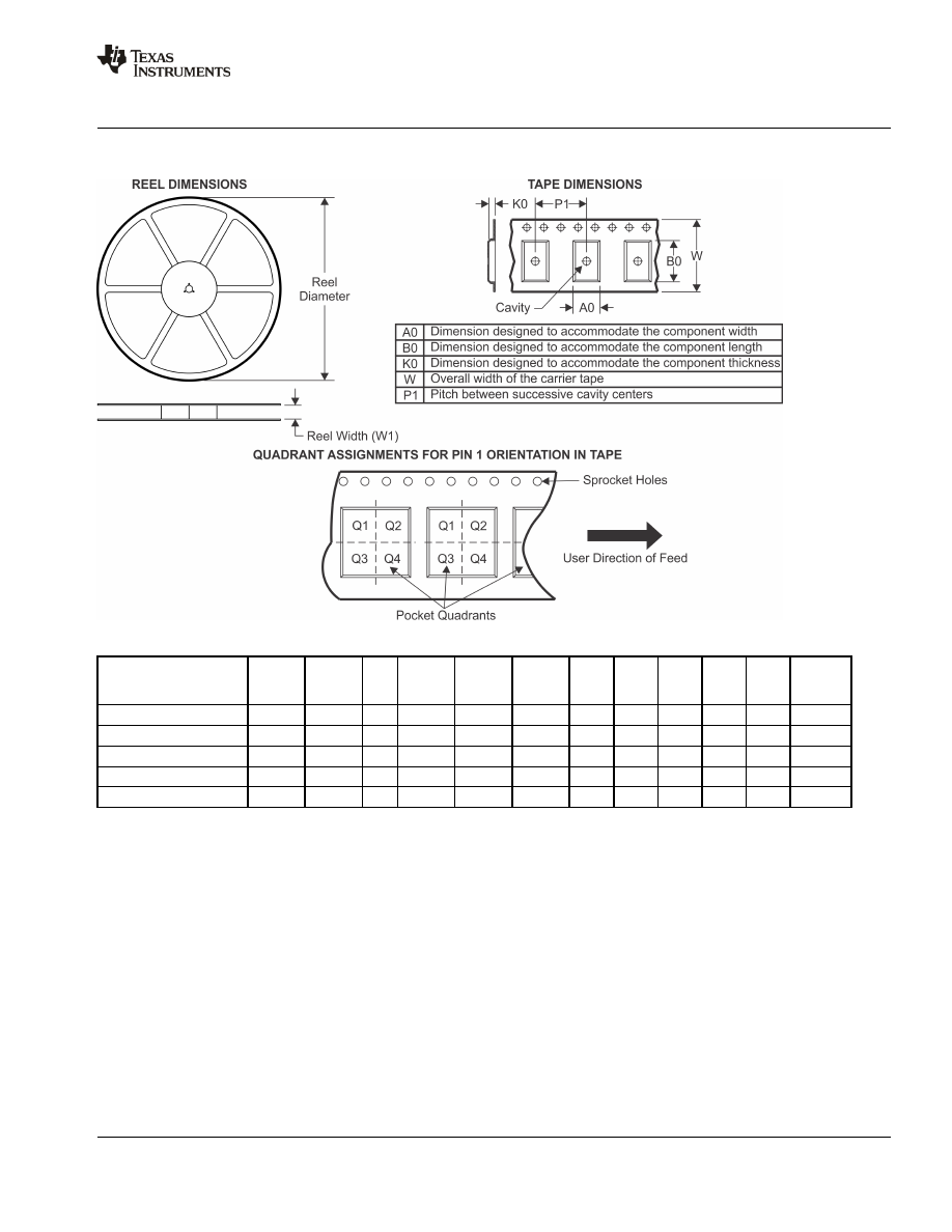
TAPE AND REEL INFORMATION
*All dimensions are nominal
Device
Package
Type
Package
Drawing
Pins
SPQ
Reel
Diameter
(mm)
Reel
Width
W1 (mm)
A0 (mm)
B0 (mm)
K0 (mm)
P1
(mm)
W
(mm)
Pin1
Quadrant
CD4049UBDR
SOIC
D
16
2500
330.0
16.4
6.5
10.3
2.1
8.0
16.0
Q1
CD4049UBDWR
SOIC
DW
16
2000
330.0
16.4
10.75
10.7
2.7
12.0
16.0
Q1
CD4049UBNSR
SO
NS
16
2000
330.0
16.4
8.2
10.5
2.5
12.0
16.0
Q1
CD4049UBPWR
TSSOP
PW
16
2000
330.0
12.4
7.0
5.6
1.6
8.0
12.0
Q1
CD4050BDR
SOIC
D
16
2500
330.0
16.4
6.5
10.3
2.1
8.0
16.0
Q1
CD4050BDWR
SOIC
DW
16
2000
330.0
16.4
10.75
10.7
2.7
12.0
16.0
Q1
CD4050BNSR
SO
NS
16
2000
330.0
16.4
8.2
10.5
2.5
12.0
16.0
Q1
CD4050BPWR
TSSOP
PW
16
2000
330.0
12.4
7.0
5.6
1.6
8.0
12.0
Q1
PACKAGE MATERIALS INFORMATION
www.ti.com
19-Mar-2008
Pack Materials-Page 1
*All dimensions are nominal
Device
Package Type
Package Drawing
Pins
SPQ
Length (mm)
Width (mm)
Height (mm)
CD4049UBDR
SOIC
D
16
2500
333.2
345.9
28.6
CD4049UBDWR
SOIC
DW
16
2000
346.0
346.0
33.0
CD4049UBNSR
SO
NS
16
2000
346.0
346.0
33.0
CD4049UBPWR
TSSOP
PW
16
2000
346.0
346.0
29.0
CD4050BDR
SOIC
D
16
2500
333.2
345.9
28.6
CD4050BDWR
SOIC
DW
16
2000
346.0
346.0
33.0
CD4050BNSR
SO
NS
16
2000
346.0
346.0
33.0
CD4050BPWR
TSSOP
PW
16
2000
346.0
346.0
29.0
PACKAGE MATERIALS INFORMATION
www.ti.com
19-Mar-2008
Pack Materials-Page 2

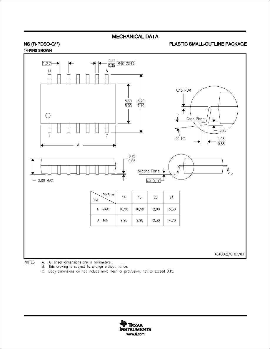
MECHANICAL DATA
MTSS001C - JANUARY 1995 - REVISED FEBRUARY 1999
POST OFFICE BOX 655303
DALLAS, TEXAS 75265
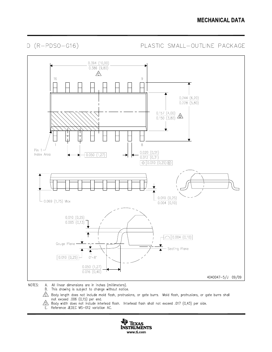
PW (R-PDSO-G**)
PLASTIC SMALL-OUTLINE PACKAGE
14 PINS SHOWN
0,65
M
0,10
0,10
0,25
0,50
0,75
0,15 NOM
Gage Plane
28
9,80
9,60
24
7,90
7,70
20
16
6,60
6,40
4040064/F 01/97
0,30
6,60
6,20
8
0,19
4,30
4,50
7
0,15
14
A
1
1,20 MAX
14
5,10
4,90
8
3,10
2,90
A MAX
A MIN
DIM
PINS **
0,05
4,90
5,10
Seating Plane
0
°
- 8
°
NOTES: A. All linear dimensions are in millimeters.
B. This drawing is subject to change without notice.
C. Body dimensions do not include mold flash or protrusion not to exceed 0,15.
D. Falls within JEDEC MO-153
PACKAGE OPTION ADDENDUM
www.ti.com
10-Aug-2016
Addendum-Page 1
PACKAGING INFORMATION
Orderable Device
Status
(1)
Package Type Package
Drawing
Pins Package
Qty
Eco Plan
(2)
Lead/Ball Finish
(6)
MSL Peak Temp
(3)
Op Temp ( °C)
Device Marking
(4/5)
Samples
CD4049UBD
ACTIVE
SOIC
D
16
40
Green (RoHS
& no Sb/Br)
CU NIPDAU
Level-1-260C-UNLIM
-55 to 125
CD4049UBM
CD4049UBDE4
ACTIVE
SOIC
D
16
40
Green (RoHS
& no Sb/Br)
CU NIPDAU
Level-1-260C-UNLIM
-55 to 125
CD4049UBM
CD4049UBDG4
ACTIVE
SOIC
D
16
40
Green (RoHS
& no Sb/Br)
CU NIPDAU
Level-1-260C-UNLIM
-55 to 125
CD4049UBM
CD4049UBDR
ACTIVE
SOIC
D
16
2500
Green (RoHS
& no Sb/Br)
CU NIPDAU
Level-1-260C-UNLIM
-55 to 125
CD4049UBM
CD4049UBDRE4
ACTIVE
SOIC
D
16
2500
Green (RoHS
& no Sb/Br)
CU NIPDAU
Level-1-260C-UNLIM
-55 to 125
CD4049UBM
CD4049UBDRG4
ACTIVE
SOIC
D
16
2500
Green (RoHS
& no Sb/Br)
CU NIPDAU
Level-1-260C-UNLIM
-55 to 125
CD4049UBM
CD4049UBDT
ACTIVE
SOIC
D
16
250
Green (RoHS
& no Sb/Br)
CU NIPDAU
Level-1-260C-UNLIM
-55 to 125
CD4049UBM
CD4049UBDW
ACTIVE
SOIC
DW
16
40
Green (RoHS
& no Sb/Br)
CU NIPDAU
Level-1-260C-UNLIM
-55 to 125
CD4049UBM
CD4049UBDWE4
ACTIVE
SOIC
DW
16
40
Green (RoHS
& no Sb/Br)
CU NIPDAU
Level-1-260C-UNLIM
-55 to 125
CD4049UBM
CD4049UBDWG4
ACTIVE
SOIC
DW
16
40
Green (RoHS
& no Sb/Br)
CU NIPDAU
Level-1-260C-UNLIM
-55 to 125
CD4049UBM
CD4049UBDWR
ACTIVE
SOIC
DW
16
TBD
Call TI
Call TI
-55 to 125
CD4049UBM
CD4049UBDWRE4
ACTIVE
SOIC
DW
16
TBD
Call TI
Call TI
-55 to 125
CD4049UBM
CD4049UBE
ACTIVE
PDIP
N
16
25
Pb-Free
(RoHS)
CU NIPDAU
N / A for Pkg Type
-55 to 125
CD4049UBE
CD4049UBEE4
ACTIVE
PDIP
N
16
25
Pb-Free
(RoHS)
CU NIPDAU
N / A for Pkg Type
-55 to 125
CD4049UBE
CD4049UBF
ACTIVE
CDIP
J
16
1
TBD
A42
N / A for Pkg Type
-55 to 125
CD4049UBF
CD4049UBF3A
ACTIVE
CDIP
J
16
1
TBD
A42
N / A for Pkg Type
-55 to 125
CD4049UBF3A
CD4049UBF3AS2283
OBSOLETE
CDIP
J
16
TBD
Call TI
Call TI
CD4049UBF3AS2534
OBSOLETE
CDIP
J
16
TBD
Call TI
Call TI
CD4049UBM
OBSOLETE
SOIC
D
16
TBD
Call TI
Call TI
-55 to 125
PACKAGE OPTION ADDENDUM
www.ti.com
10-Aug-2016
Addendum-Page 2
Orderable Device
Status
(1)
Package Type Package
Drawing
Pins Package
Qty
Eco Plan
(2)
Lead/Ball Finish
(6)
MSL Peak Temp
(3)
Op Temp ( °C)
Device Marking
(4/5)
Samples
CD4049UBM96
OBSOLETE
SOIC
D
16
TBD
Call TI
Call TI
-55 to 125
CD4049UBNSR
ACTIVE
SO
NS
16
2000
Green (RoHS
& no Sb/Br)
CU NIPDAU
Level-1-260C-UNLIM
-55 to 125
CD4049UB
CD4049UBNSRG4
ACTIVE
SO
NS
16
2000
Green (RoHS
& no Sb/Br)
CU NIPDAU
Level-1-260C-UNLIM
-55 to 125
CD4049UB
CD4049UBPW
ACTIVE
TSSOP
PW
16
90
Green (RoHS
& no Sb/Br)
CU NIPDAU
Level-1-260C-UNLIM
-55 to 125
CM049UB
CD4049UBPWG4
ACTIVE
TSSOP
PW
16
90
Green (RoHS
& no Sb/Br)
CU NIPDAU
Level-1-260C-UNLIM
-55 to 125
CM049UB
CD4049UBPWR
ACTIVE
TSSOP
PW
16
2000
Green (RoHS
& no Sb/Br)
CU NIPDAU
Level-1-260C-UNLIM
-55 to 125
CM049UB
CD4049UBPWRE4
ACTIVE
TSSOP
PW
16
2000
Green (RoHS
& no Sb/Br)
CU NIPDAU
Level-1-260C-UNLIM
-55 to 125
CM049UB
CD4050BD
ACTIVE
SOIC
D
16
40
Green (RoHS
& no Sb/Br)
CU NIPDAU
Level-1-260C-UNLIM
-55 to 125
CD4050BM
CD4050BDE4
ACTIVE
SOIC
D
16
40
Green (RoHS
& no Sb/Br)
CU NIPDAU
Level-1-260C-UNLIM
-55 to 125
CD4050BM
CD4050BDR
ACTIVE
SOIC
D
16
2500
Green (RoHS
& no Sb/Br)
CU NIPDAU
Level-1-260C-UNLIM
-55 to 125
CD4050BM
CD4050BDRG4
ACTIVE
SOIC
D
16
2500
Green (RoHS
& no Sb/Br)
CU NIPDAU
Level-1-260C-UNLIM
-55 to 125
CD4050BM
CD4050BDT
ACTIVE
SOIC
D
16
250
Green (RoHS
& no Sb/Br)
CU NIPDAU
Level-1-260C-UNLIM
-55 to 125
CD4050BM
CD4050BDW
ACTIVE
SOIC
DW
16
40
Green (RoHS
& no Sb/Br)
CU NIPDAU
Level-1-260C-UNLIM
-55 to 125
CD4050BM
CD4050BDWR
ACTIVE
SOIC
DW
16
2000
Green (RoHS
& no Sb/Br)
CU NIPDAU
Level-1-260C-UNLIM
-55 to 125
CD4050BM
CD4050BDWRE4
ACTIVE
SOIC
DW
16
2000
Green (RoHS
& no Sb/Br)
CU NIPDAU
Level-1-260C-UNLIM
-55 to 125
CD4050BM
CD4050BE
ACTIVE
PDIP
N
16
25
Pb-Free
(RoHS)
CU NIPDAU
N / A for Pkg Type
-55 to 125
CD4050BE
CD4050BEE4
ACTIVE
PDIP
N
16
25
Pb-Free
(RoHS)
CU NIPDAU
N / A for Pkg Type
-55 to 125
CD4050BE
CD4050BF
ACTIVE
CDIP
J
16
1
TBD
A42
N / A for Pkg Type
-55 to 125
CD4050BF
CD4050BF3A
ACTIVE
CDIP
J
16
1
TBD
A42
N / A for Pkg Type
-55 to 125
CD4050BF3A
PACKAGE OPTION ADDENDUM
www.ti.com
10-Aug-2016
Addendum-Page 3
Orderable Device
Status
(1)
Package Type Package
Drawing
Pins Package
Qty
Eco Plan
(2)
Lead/Ball Finish
(6)
MSL Peak Temp
(3)
Op Temp ( °C)
Device Marking
(4/5)
Samples
CD4050BF3AS2283
OBSOLETE
CDIP
J
16
TBD
Call TI
Call TI
CD4050BF3AS2534
OBSOLETE
CDIP
J
16
TBD
Call TI
Call TI
CD4050BM
OBSOLETE
SOIC
D
16
TBD
Call TI
Call TI
-55 to 125
CD4050BNSR
ACTIVE
SO
NS
16
2000
Green (RoHS
& no Sb/Br)
CU NIPDAU
Level-1-260C-UNLIM
-55 to 125
CD4050B
CD4050BPW
ACTIVE
TSSOP
PW
16
90
Green (RoHS
& no Sb/Br)
CU NIPDAU
Level-1-260C-UNLIM
-55 to 125
CM050B
CD4050BPWR
ACTIVE
TSSOP
PW
16
2000
Green (RoHS
& no Sb/Br)
CU NIPDAU
Level-1-260C-UNLIM
-55 to 125
CM050B
CD4050BPWRE4
ACTIVE
TSSOP
PW
16
2000
Green (RoHS
& no Sb/Br)
CU NIPDAU
Level-1-260C-UNLIM
-55 to 125
CM050B
JM38510/05553BEA
ACTIVE
CDIP
J
16
1
TBD
A42
N / A for Pkg Type
-55 to 125
JM38510/
05553BEA
JM38510/05554BEA
ACTIVE
CDIP
J
16
1
TBD
A42
N / A for Pkg Type
-55 to 125
JM38510/
05554BEA
M38510/05553BEA
ACTIVE
CDIP
J
16
1
TBD
A42
N / A for Pkg Type
-55 to 125
JM38510/
05553BEA
M38510/05554BEA
ACTIVE
CDIP
J
16
1
TBD
A42
N / A for Pkg Type
-55 to 125
JM38510/
05554BEA
(1)
The marketing status values are defined as follows:
ACTIVE: Product device recommended for new designs.
LIFEBUY: TI has announced that the device will be discontinued, and a lifetime-buy period is in effect.
NRND: Not recommended for new designs. Device is in production to support existing customers, but TI does not recommend using this part in a new design.
PREVIEW: Device has been announced but is not in production. Samples may or may not be available.
OBSOLETE: TI has discontinued the production of the device.
(2)
Eco Plan - The planned eco-friendly classification: Pb-Free (RoHS), Pb-Free (RoHS Exempt), or Green (RoHS & no Sb/Br) - please check
for the latest availability
information and additional product content details.
TBD: The Pb-Free/Green conversion plan has not been defined.
Pb-Free (RoHS): TI's terms "Lead-Free" or "Pb-Free" mean semiconductor products that are compatible with the current RoHS requirements for all 6 substances, including the requirement that
lead not exceed 0.1% by weight in homogeneous materials. Where designed to be soldered at high temperatures, TI Pb-Free products are suitable for use in specified lead-free processes.
Pb-Free (RoHS Exempt): This component has a RoHS exemption for either 1) lead-based flip-chip solder bumps used between the die and package, or 2) lead-based die adhesive used between
the die and leadframe. The component is otherwise considered Pb-Free (RoHS compatible) as defined above.
Green (RoHS & no Sb/Br): TI defines "Green" to mean Pb-Free (RoHS compatible), and free of Bromine (Br) and Antimony (Sb) based flame retardants (Br or Sb do not exceed 0.1% by weight
in homogeneous material)
(3)
MSL, Peak Temp. - The Moisture Sensitivity Level rating according to the JEDEC industry standard classifications, and peak solder temperature.
PACKAGE OPTION ADDENDUM
www.ti.com
10-Aug-2016
Addendum-Page 4
(4)
There may be additional marking, which relates to the logo, the lot trace code information, or the environmental category on the device.
(5)
Multiple Device Markings will be inside parentheses. Only one Device Marking contained in parentheses and separated by a "~" will appear on a device. If a line is indented then it is a continuation
of the previous line and the two combined represent the entire Device Marking for that device.
(6)
Lead/Ball Finish - Orderable Devices may have multiple material finish options. Finish options are separated by a vertical ruled line. Lead/Ball Finish values may wrap to two lines if the finish
value exceeds the maximum column width.
Important Information and Disclaimer:The information provided on this page represents TI's knowledge and belief as of the date that it is provided. TI bases its knowledge and belief on information
provided by third parties, and makes no representation or warranty as to the accuracy of such information. Efforts are underway to better integrate information from third parties. TI has taken and
continues to take reasonable steps to provide representative and accurate information but may not have conducted destructive testing or chemical analysis on incoming materials and chemicals.
TI and TI suppliers consider certain information to be proprietary, and thus CAS numbers and other limited information may not be available for release.
In no event shall TI's liability arising out of such information exceed the total purchase price of the TI part(s) at issue in this document sold by TI to Customer on an annual basis.
OTHER QUALIFIED VERSIONS OF CD4049UB, CD4049UB-MIL, CD4050B, CD4050B-MIL :
Catalog:
,
Military:
,
NOTE: Qualified Version Definitions:
Catalog - TI's standard catalog product
Military - QML certified for Military and Defense Applications
TAPE AND REEL INFORMATION
*All dimensions are nominal
Device
Package
Type
Package
Drawing
Pins
SPQ
Reel
Diameter
(mm)
Reel
Width
W1 (mm)
A0
(mm)
B0
(mm)
K0
(mm)
P1
(mm)
W
(mm)
Pin1
Quadrant
CD4049UBDR
SOIC
D
16
2500
330.0
16.4
6.5
10.3
2.1
8.0
16.0
Q1
CD4049UBPWR
TSSOP
PW
16
2000
330.0
12.4
6.9
5.6
1.6
8.0
12.0
Q1
CD4050BDR
SOIC
D
16
2500
330.0
16.4
6.5
10.3
2.1
8.0
16.0
Q1
CD4050BDWR
SOIC
DW
16
2000
330.0
16.4
10.75
10.7
2.7
12.0
16.0
Q1
CD4050BPWR
TSSOP
PW
16
2000
330.0
12.4
6.9
5.6
1.6
8.0
12.0
Q1
PACKAGE MATERIALS INFORMATION
www.ti.com
10-Aug-2016
Pack Materials-Page 1
*All dimensions are nominal
Device
Package Type
Package Drawing
Pins
SPQ
Length (mm)
Width (mm)
Height (mm)
CD4049UBDR
SOIC
D
16
2500
333.2
345.9
28.6
CD4049UBPWR
TSSOP
PW
16
2000
367.0
367.0
35.0
CD4050BDR
SOIC
D
16
2500
333.2
345.9
28.6
CD4050BDWR
SOIC
DW
16
2000
367.0
367.0
38.0
CD4050BPWR
TSSOP
PW
16
2000
367.0
367.0
35.0
PACKAGE MATERIALS INFORMATION
www.ti.com
10-Aug-2016
Pack Materials-Page 2


IMPORTANT NOTICE
Texas Instruments Incorporated and its subsidiaries (TI) reserve the right to make corrections, enhancements, improvements and other
changes to its semiconductor products and services per JESD46, latest issue, and to discontinue any product or service per JESD48, latest
issue. Buyers should obtain the latest relevant information before placing orders and should verify that such information is current and
complete. All semiconductor products (also referred to herein as components) are sold subject to TIs terms and conditions of sale
supplied at the time of order acknowledgment.
TI warrants performance of its components to the specifications applicable at the time of sale, in accordance with the warranty in TIs terms
and conditions of sale of semiconductor products. Testing and other quality control techniques are used to the extent TI deems necessary
to support this warranty. Except where mandated by applicable law, testing of all parameters of each component is not necessarily
performed.
TI assumes no liability for applications assistance or the design of Buyers products. Buyers are responsible for their products and
applications using TI components. To minimize the risks associated with Buyers products and applications, Buyers should provide
adequate design and operating safeguards.
TI does not warrant or represent that any license, either express or implied, is granted under any patent right, copyright, mask work right, or
other intellectual property right relating to any combination, machine, or process in which TI components or services are used. Information
published by TI regarding third-party products or services does not constitute a license to use such products or services or a warranty or
endorsement thereof. Use of such information may require a license from a third party under the patents or other intellectual property of the
third party, or a license from TI under the patents or other intellectual property of TI.
Reproduction of significant portions of TI information in TI data books or data sheets is permissible only if reproduction is without alteration
and is accompanied by all associated warranties, conditions, limitations, and notices. TI is not responsible or liable for such altered
documentation. Information of third parties may be subject to additional restrictions.
Resale of TI components or services with statements different from or beyond the parameters stated by TI for that component or service
voids all express and any implied warranties for the associated TI component or service and is an unfair and deceptive business practice.
TI is not responsible or liable for any such statements.
Buyer acknowledges and agrees that it is solely responsible for compliance with all legal, regulatory and safety-related requirements
concerning its products, and any use of TI components in its applications, notwithstanding any applications-related information or support
that may be provided by TI. Buyer represents and agrees that it has all the necessary expertise to create and implement safeguards which
anticipate dangerous consequences of failures, monitor failures and their consequences, lessen the likelihood of failures that might cause
harm and take appropriate remedial actions. Buyer will fully indemnify TI and its representatives against any damages arising out of the use
of any TI components in safety-critical applications.
In some cases, TI components may be promoted specifically to facilitate safety-related applications. With such components, TIs goal is to
help enable customers to design and create their own end-product solutions that meet applicable functional safety standards and
requirements. Nonetheless, such components are subject to these terms.
No TI components are authorized for use in FDA Class III (or similar life-critical medical equipment) unless authorized officers of the parties
have executed a special agreement specifically governing such use.
Only those TI components which TI has specifically designated as military grade or enhanced plastic are designed and intended for use in
military/aerospace applications or environments. Buyer acknowledges and agrees that any military or aerospace use of TI components
which have not been so designated is solely at the Buyer's risk, and that Buyer is solely responsible for compliance with all legal and
regulatory requirements in connection with such use.
TI has specifically designated certain components as meeting ISO/TS16949 requirements, mainly for automotive use. In any case of use of
non-designated products, TI will not be responsible for any failure to meet ISO/TS16949.
Products
Applications
Audio
Automotive and Transportation
Amplifiers
Communications and Telecom
Data Converters
Computers and Peripherals
DLP ® Products
Consumer Electronics
DSP
Energy and Lighting
Clocks and Timers
Industrial
Interface
Medical
Logic
Security
Power Mgmt
Space, Avionics and Defense
Microcontrollers
Video and Imaging
RFID
OMAP Applications Processors
TI E2E Community
Wireless Connectivity
Mailing Address: Texas Instruments, Post Office Box 655303, Dallas, Texas 75265
Copyright © 2016, Texas Instruments Incorporated

