| Secciones |
|---|
| Foros Electrónica |
|
|
| Boletines de correo |
 |
EL2004/EL2004C
November
1993
Rev
G
EL2004/EL2004C
350 MHz FET Buffer
Note: All information contained in this data sheet has been carefully checked and is believed to be accurate as of the date of publication; however, this data sheet cannot be a controlled document. Current revisions, if any, to these
specifications are maintained at the factory and are available upon your request. We recommend checking the revision level before finalization of your design documentation. Patent pending.
©
1989 Elantec, Inc.
Features
# Slew rateÃ2500 V/ms
# Rise timeÃ1 ns
# BandwidthÃ350 MHz
# ELH0033Ãpin compatible
#
g
5 to
g
15V operation
# 100 mA output current
# MIL-STD-883B Rev. C devices
manufactured in U.S.A.
Applications
# Coaxial cable driver
# Fast op amp booster
# Flash converter driver
# Video line driver
# High-speed sample and hold
# Pulse transformer driver
# A.T.E. pin driver
Ordering Information
Part No.
Temp. Range
Package Outline
Ã
EL2004CG
b
25
§
C to
a
85
§
C
TO-8
MDP0002
EL2004G
b
55
§
C to
a
125
§
C
TO-8
MDP0002
EL2004L
b
55
§
C to
a
125
§
C 52-Pad LCC MDP0013
EL2004L/MIL
b
55
§
C to
a
125
§
C 52-Pad LCC MDP0013
5962-89659 is the SMD version of this device.
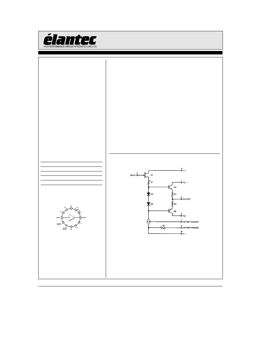
Connection Diagram
Case is Electrically Isolated
2004 - 1
Top View
General Description
The EL2004 is a very high-speed, FET input buffer/line driver
designed for unity gain applications at both high current (up to
100 mA) and at frequencies up to 350 MHz. The 2500 V/
ms slew
rate and wide bandwidth ensures the stability of the circuit
when the EL2004 is used inside op amp feedback loops.
Applications for the EL2004 include line drivers, video buffers,
wideband instrumentation, and high-speed drivers for inductive
and capacitive loads. The performance of the EL2004 makes it
an ideal buffer for video applications including input buffers for
flash A/D converters, and output buffers for video DACs. Its
excellent phase linearity is particularly advantageous in digital
signal processing applications.
Elantec facilities comply with MIL-I-45208A and are MIL-
STD-1772 certified. Elantecs Military devices comply with
MIL-STD-883B Revision C and are manufactured in our rigidly
controlled, ultra-clean facilities in Milpitas, California. For ad-
ditional information on Elantecs Quality and Reliability Assur-
ance Policy and procedures request brochure QRA-1.
Simplified Schematic
2004 - 3
EL2004/EL2004C
350 MHz FET Buffer
Absolute Maximum Ratings
(T
A
e
25
§
C)
V
S
Supply Voltage (V
a b
V
b
)
40V
V
IN
Input Voltage
40V
P
D
Power Dissipation (See curves)
1.5W
I
OC
Continuous Output Current
g
100 mA
I
OP
Peak Output Current
g
250 mA
T
A
Operating Temperature Range
EL2004
b
55
§
C to
a
125
§
C
EL2004C
b
25
§
C to
a
85
§
C
T
J
Operating Junction Temperature
175
§
C
T
ST
Storage Temperature
b
65
§
C to
a
150
§
C
Lead Temperature
(Soldering, 10 seconds)
300
§
C
Important Note:
All parameters having Min/Max specifications are guaranteed. The Test Level column indicates the specific device testing actually
performed during production and Quality inspection. Elantec performs most electrical tests using modern high-speed automatic test
equipment, specifically the LTX77 Series system. Unless otherwise noted, all tests are pulsed tests, therefore T
J
e
T
C
e
T
A
.
Test Level
Test Procedure
I
100% production tested and QA sample tested per QA test plan QCX0002.
II
100% production tested at T
A
e
25
§
C and QA sample tested at T
A
e
25
§
C ,
T
MAX
and T
MIN
per QA test plan QCX0002.
III
QA sample tested per QA test plan QCX0002.
IV
Parameter is guaranteed (but not tested) by Design and Characterization Data.
V
Parameter is typical value at T
A
e
25
§
C for information purposes only.
g
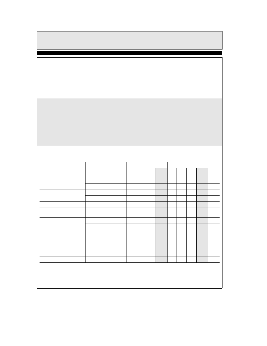
15V DC Electrical Characteristics
V
S
e
g
15V, T
MIN
k
T
A
k
T
MAX
, V
IN
e
0V, R
L
e
1 k
X unless otherwise specified (Note 1)
Parameter
Description
Test Conditions
EL2004
EL2004C
Units
Min
Typ
Max
Test
Min
Typ
Max
Test
Level
Level
V
OS
Output Offset
R
S
s
100 k
X, T
J
e
25
§
C
5
10
I
12
20
I
mV
Voltage
R
S
s
100 k
X
15
I
25
III
mV
A
V
Voltage Gain
V
IN
e
g
10V
0.97
0.98
1.0
I
0.96
0.98
1.0
II
V/V
R
L
e
100
X, V
IN
e
g
10V
0.92
0.95
0.98
I
0.90
0.95
0.98
II
V/V
R
IN
Input Impedance
T
J
e
25
§
C, V
IN
e
g
1V
10
8
10
11
I
10
8
10
11
I
X
R
OUT
Output
V
IN
e
g
1 V
DC
,
4
8
I
4
10
II
X
Impedance
DR
L
e
100
X to Infinity
V
O
Output Voltage
V
IN
e
g
14V
g
12
g
13
I
g
12
g
13
II
V
Swing
V
IN
e
g
10.5V, R
L
e
100
X
g
9
g
9.8
I
g
9
g
9.8
I
V
T
A
e
25
§
C
I
IN
Input Current
T
J
e
25
§
C (Note 2)
0.25
I
2.0
I
nA
T
A
e
25
§
C (Note 3)
2.5
IV
20
IV
nA
T
J
e
T
A
e
T
MAX
10
I
50
III
nA
V
IN
e b
10V
20
V
20
V
nA
I
S
Supply Current
20
24
I
20
24
II
mA
2
TD
is
3.2in
EL2004/EL2004C
350 MHz FET Buffer
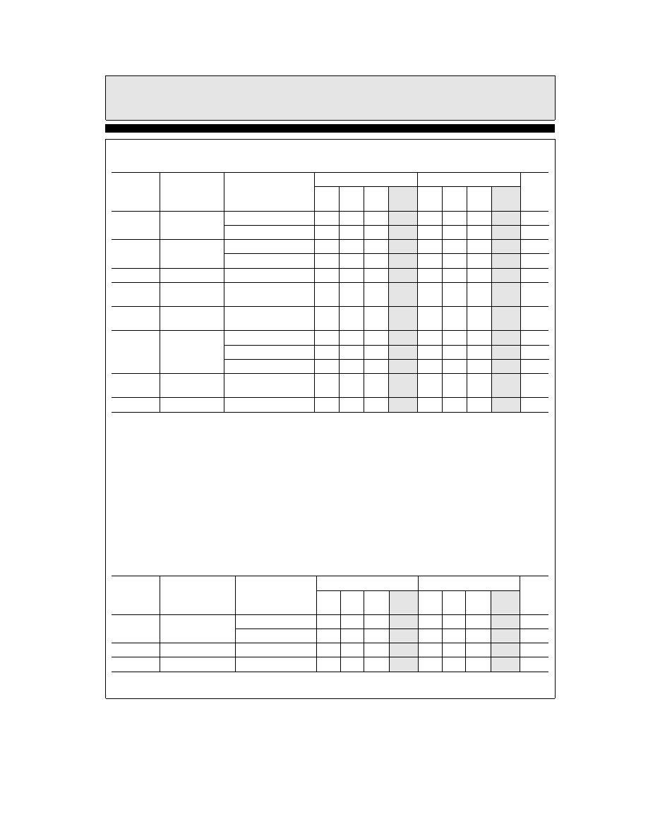
g
5V DC Electrical Characteristics
V
S
e
g
5V, T
MIN
k
T
A
k
T
MAX
, V
IN
e
0V, R
L
e
50
X unless otherwise specified
Parameter
Description
Test Conditions
EL2004
EL2004C
Units
Min
Typ
Max
Test
Min
Typ
Max
Test
Level
Level
V
OS
Output Offset
R
S
s
100 k
X, T
J
e
25
§
C
10
30
I
10
30
I
mV
Voltage
R
S
s
100 k
X
35
I
35
III
mV
A
V
Voltage Gain
V
IN
e
g
1V, R
L
e
1 k
X
0.90
0.95
1.0
I
0.90
0.95
1.0
II
V/V
V
IN
e
g
1V
0.80
0.88
0.95
I
0.80
0.88
0.95
II
V/V
R
IN
Input Impedance
T
J
e
25
§
C, V
IN
e
g
1V
10
8
10
11
I
10
10
10
11
I
X
R
OUT
Output
V
IN
e
g
1 V
DC
,
4
8
I
4
10
II
X
Impedance
DR
L
e
50
X to Infinity
V
O
Output Voltage
V
IN
e
g
4V
g
2.0
g
2.9
I
g
2.0
g
2.9
III
V
Swing
I
IN
Input Current
T
J
e
25
§
C (Note 2)
250
I
500
I
pA
T
A
e
25
§
C (Note 3)
2.5
IV
5
IV
nA
T
J
e
T
A
e
T
MAX
10
I
20
III
nA
PSRR
Power Supply
V
S
e
g
5V to
g
15V
60
V
60
V
dB
Rejection Ratio
R
L
e
1 k
X
I
S
Supply Current
R
L
e
1 k
X
17.5
20
I
17.5
20
II
mA
Note 1: When operating at elevated temperatures the power dissipation of the EL2004 must be limited to the values shown in the
typical performance curve Maximum Power Dissipation vs Temperature. Junction to case thermal resistance is 31
§
C/W
when dissipation is spread among the transistors in a normal AC steady-state condition. In special conditions where heat is
concentrated in one output device, junction temperature should be calculated using a thermal resistance of 70
§
C/W.
Note 2: Specification is at 25
§
C junction temperature due to requirements of high-speed automatic testing. Actual values at operating
temperatures will exceed the value at T
J
e
25
§
C. When supply voltages are
g
15V, no-load operating junction temperatures
may rise 40
§
C to 60
§
C above ambient and more under load conditions. Accordingly, V
OS
may change one to several mV, and
I
IN
will change significantly during warm-up. Refer to I
IN
vs Temperature graph for expected values.
Note 3: Measured in still air seven minutes after application of power. See graph of Input Current During Warm-up for further
information.
Note 4: Bandwidth is calculated from the rise time. The EL2004 has a single pole gain and phase response up to the
b
3 dB
frequency.
Note 5: Slew rate is measured between V
OUT
e a
2.5V and
b
2.5V for this test.
Note 6: Slew rate is measured between V
OUT
e a
1V and
b
1V for this test. Pulse repetition rate is
k
50 MHz.
g
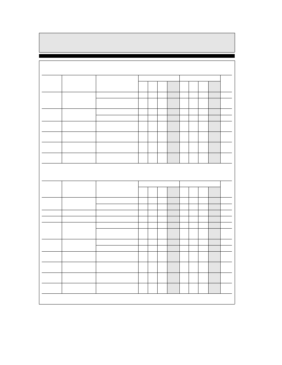
15V AC Electrical Characteristics
V
S
e
g
15V, R
L
e
1 k
X, R
S
e
50
X, T
J
e
25
§
C unless otherwise specified
Parameter
Description
Test Conditions
EL2004
EL2004C
Units
Min
Typ
Max
Test
Min
Typ
Max
Test
Level
Level
BW
Bandwidth
(Note 4)
200
350
I
200
350
I
MHz
R
L
e
50
X
140
200
I
140
200
I
MHz
t
s
Settling Time to 1%
DV
IN
e
1V, t
r
e
3 ns
6
V
6
V
ns
C
in
Input Capacitance
3
V
3
V
pF
3
TD
is
3.2in
TD
is
1.3in
EL2004/EL2004C
350 MHz FET Buffer
g
15V AC Electrical Characteristics
V
S
e
g
15V, R
L
e
1 k
X, R
S
e
50
X, T
J
e
25
§
C unless otherwise specified
à Contd.
Parameter
Description
Test Conditions
EL2004
EL2004C
Units
Min Typ Max
Test
Min Typ Max
Test
Level
Level
SR
Slew Rate
V
IN
e
g
5V (Note 5)
2000
2500
I
2000
2500
I
V/
ms
C
L
e
100 pF, V
IN
e
g
5V
1200
V
1200
V
V/
ms
(Note 5)
t
r
Rise Time
DV
IN
P 0.6V
1.0
1.7
I
1.0
1.7
I
ns
Note: See Test Figure
DV
IN
P 0.6V, R
L
e
50
X
1.7
2.5
I
1.7
2.5
I
ns
t
p
Propagation Delay
DV
IN
P 0.6V
1.0
2.0
I
1.0
2.0
I
ns
Note: See Test Figure
R
OUT
Output
f
e
1 MHz, V
IN
e
1 V
RMS
4
V
4
V
X
Impedance
DR
L
e
100
X to Infinity
a
PSRR
Power Supply
DV
S
a e
g
1.5 V
peak
40
V
40
V
dB
Rejection Ratio
f
e
1 kHz
b
PSRR
Power Supply
DV
S
b e
g
1.5 V
peak
40
V
40
V
dB
Rejection Ratio
f
e
1 kHz
g
5V AC Electrical Characteristics
V
S
e
g
5V, R
L
e
50
X, R
S
e
50
X, T
J
e
25
§
C unless otherwise specified
Parameter
Description
Test Conditions
EL2004
EL2004C
Units
Min Typ Max
Test
Min Typ Max
Test
Level
Level
BW
Bandwidth
R
L
e
1 k
X
175
220
I
175
220
I
MHz
(Note 4)
125
150
IV
125
150
IV
MHz
t
s
Settling Time to 1%
DV
IN
e
1V, t
r
e
3 ns
8
V
8
V
ns
C
in
Input Capacitance
3
V
3
V
pF
SR
Slew Rate
V
IN
e
g
2V (Note 6)
900
1200
I
900
1200
I
V/
ms
C
L
e
100 pF, V
IN
e
g
2V
500
V
500
V
V/
ms
R
L
e
1 k
X (Note 6)
t
r
Rise Time
R
L
e
1 k
X, DV
IN
P 0.6V
1.6
2.0
I
1.6
2.0
I
ns
Note: See Test Figure
R
L
e
50
X, DV
IN
P 0.6V
2.3
2.8
IV
2.3
2.8
IV
ns
t
p
Propagation Delay
R
L
e
1 k
X, DV
IN
P 0.6V
1.2
2.4
I
1.2
2.4
I
ns
Note: See Test Figure
R
OUT
Output
f
e
1 MHz, V
IN
e
1 V
RMS
4
V
4
V
X
Impedance
DR
L
e
100
X to Infinity
a
PSRR
Power Supply
DV
S
b e
g
0.5 V
peak
30
V
30
V
dB
Rejection Ratio
f
e
1 kHz
b
PSRR
Power Supply
DV
S
a e
g
0.5 V
peak
30
V
30
V
dB
Rejection Ratio
f
e
1 kHz
4
TD
is
2.7in
TD
is
3.4in
EL2004/EL2004C
350 MHz FET Buffer
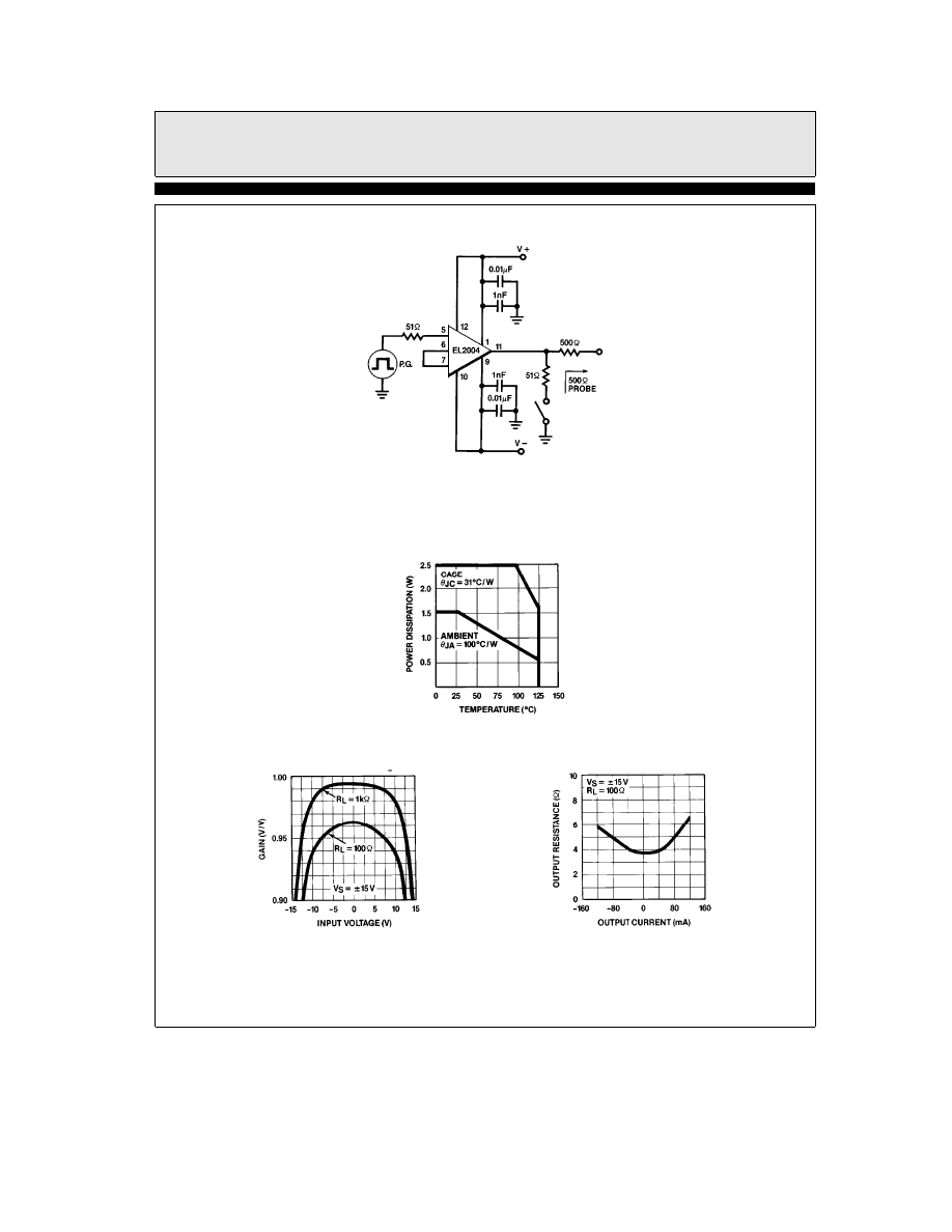
AC Test Circuit
2004 - 4
Typical Performance Curves
Dissipation
Maximum Power
TO-8
2004 - 5
Gain vs Input Voltage
Output Current
Output Resistance vs
2004 - 7
5
EL2004/EL2004C
350 MHz FET Buffer
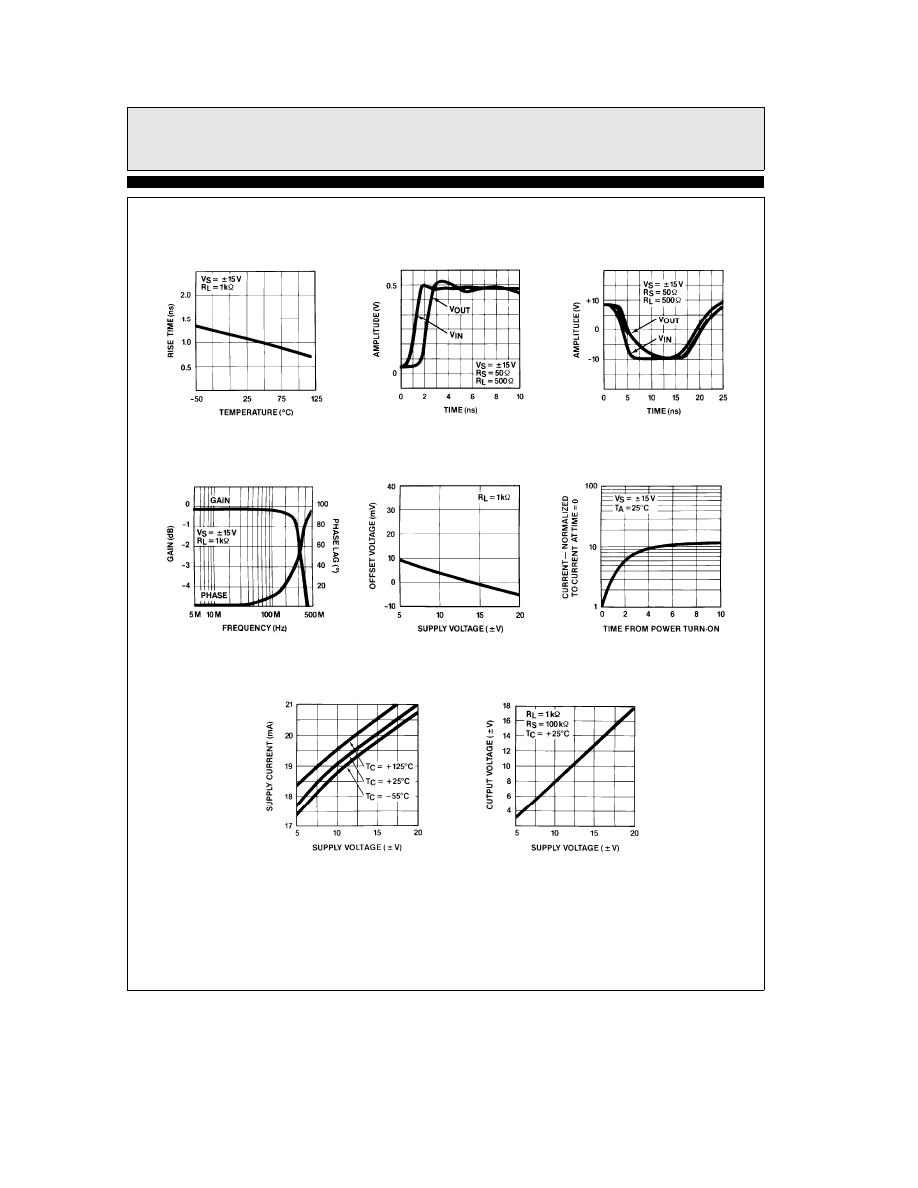
Typical Performance Curves
à Contd.
Temperature
Rise Time vs
Response
Small Signal Pulse
Response
Large Signal Pulse
Frequency Response
Voltage
Offset Voltage vs Supply
Warm-up
Current During
Normalized Input Bias
Supply Voltage
Supply Current vs
Supply Voltage
Output Voltage vs
2004 - 8
6
EL2004/EL2004C
350 MHz FET Buffer
Applications Information
The EL2004 is one member of a family of high
performance buffers manufactured by Elantec.
The 2004 is optimized for speed while others offer
choices of input DC parameters or output drive
or cost. The following table illustrates those
members available at the time of this printing.
Consult the factory for the latest capabilities in
this developing line.
Elantecs Buffer Family
Slew
Bandwidth
Input
Peak
Rise
Part
Ã
Rate
MHz
Current
I
OUT
Time
V/ms
(Warm)
mA
ns
ELH0002
200
50
6
mA
400
7
ELH0033
1500
100
2.5 nA
250
2.9
EL2004
2500
350
2.5 nA
250
1.0
EL2005
1500
140
0.1 nA
250
2.5
Recommended Layout Precautions
The very high-speed performance of the EL2004
can only be realized by taking certain precau-
tions in circuit layout and power supply decou-
pling. Low inductance ceramic chip or disc power
supply decoupling capacitors of 0.1
mF or more
should be connected with the shortest practical
lead lengths between the device supply leads and
a ground plane. In addition, it can be helpful to
parallel these with 4.7
mF electrolytics (Tanta-
lum preferred). Failure to follow these precau-
tions can result in oscillation.
Circuit Operation
The EL2004 is effectively an ideal unity gain am-
plifier with almost infinite input impedance and
about 6
X output impedance.
Input Characteristics
The input impedance of a junction FET is a
strong function of temperature and input volt-
age. Nominal input resistance of EL2004 is 10
12
at 25
§
C junction, but as I
B
doubles every 11
§
C in
the JFET, the input resistance falls. During
warm-up, self-heating raises the junction temper-
ature up to 60
§
C or more (without heatsink) so
operating I
B
will be much higher than the data
sheet 25
§
C specification.
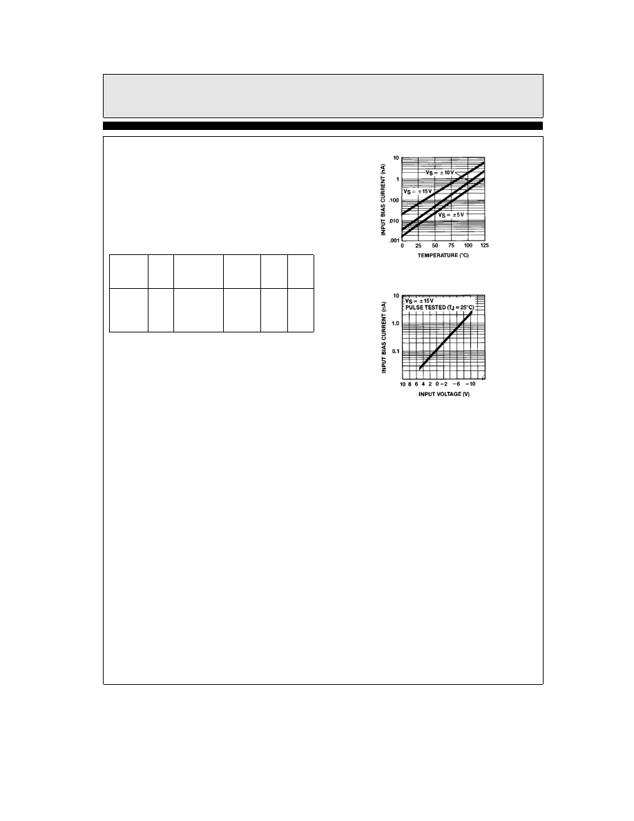
Another factor which can increase bias current is
input voltage. If the input voltage is more than
20V below the positive supply, the input current
rises exponentially. (See Curve.)
Input Bias Current vs
Temperature
Input Voltage
Input Bias Current vs
2004 - 9
In applications such as sample and hold circuits
where it is important to maintain low input bias
current over input voltage range, the EL2005
High Accuracy Fast Buffer is recommended.
The input capacitance of EL2004 comprises the
FET device gate-to-source capacitance (which is
a function of input voltage) and stray capaci-
tance to the case. Effective input capacitance can
be minimized by connecting the case to the out-
put since it is electrically isolated. Or, for reduced
radiation, the case may be grounded. The AC
characteristics specified in this data sheet were
obtained with the case floating.
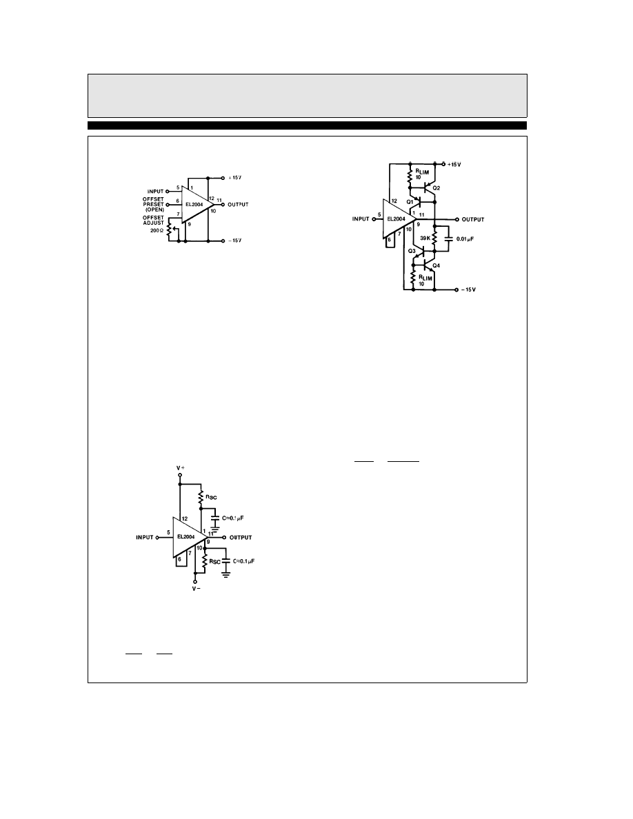
Offset Voltage Adjustment
The EL2004s offset voltages have been actively
laser trimmed at
g
15V supplies to meet specified
limits when the offset adjust pin is shorted to the
offset preset pin. If external offset null is re-
quired, the offset adjust pin should be connected
to a 200
X trim pot connected to the negative sup-
ply.
7
EL2004/EL2004C
350 MHz FET Buffer
Circuit Operation
à Contd.
Offset Zero Adjust
2004 - 10
Capacitive Loading
The EL2004 is designed to drive capacitive loads
up to several thousand picofarads without oscil-
lation. However, peak current resulting from
charging currents on fast edges should be limited
below the absolute maximum peak current rating
of 250 mA. In some cases it may be necessary to
employ one of the current limit schemes shown
below.
Short Circuit Protection
Dynamic response of the EL2004 was preserved
by excluding current limit circuits which are not
needed in most applications. However, in situa-
tions where operating conditions are not con-
trolled, short circuit protection can be added by
inserting resistors between the output device col-
lectors and supplies as illustrated.
Using Resistor
Current Limiting
2004 - 11
Suitable resistor values can be calculated as fol-
lows:
R
SC
e
V
a
I
SC
e
V
b
I
SC
where I
SC
s
100 mA for EL2004.
Current Limiting
Using Current Sources
2004 - 12
The inclusion of limiting resistors in the collec-
tors of the output devices will reduce the output
voltage swing and speed. Decoupling V
C
a
and
V
C
b
pins with capacitors to ground will retain
full output swing for transient pulses.
An alternate active current limit technique that
retains full DC output swing is shown above.
Here the current sources are saturated during
normal operation thus applying full supply volt-
age to the V
C
pins. Under fault conditions, the
voltage decreases as the current source reaches its
limit.
R
LIM
e
V
BE
I
SC
e
0.6V
100 mA
e
6
X
Power Supplies
The EL2004 has been characterized for both
g
15
and
g
5V dual supply operation, but other combi-
nations can also be useful. For example, in many
video applications it is only necessary for the out-
put to swing
g
2V or less, but speed and distor-
tion are important. In this situation, the input
stage can be operated at the full
g
15V supply
while the output collectors are returned to
g
5V.
The speed and distortion will be almost as good
as if the whole circuit was operating at
g
15V,
but the dissipation is substantially reduced and
higher load currents can be safely accommodat-
ed.
8
EL2004/EL2004C
350 MHz FET Buffer
Circuit Operation
à Contd.
Increasing Operating Voltage
and Reducing Thermal Tail
When driving heavy loads, the changing dissipa-
tion in the output transistors can sometimes
cause temperature gradients in the circuit which
cause a shift in offset voltage and the phenome-
non known as thermal tail. Bootstrapping the
output as illustrated substantially reduces the
power in the output transistors and mitigates the
effect.
High Voltage Inputs can be Accommodated
with Bootstrapped Supplies
2004 - 13
Hardware
In order to utilize the full drive capabilities of the
EL2004, it should be mounted with a heatsink,
particularly for extended temperature operation.
Suitable heatsinks include Thermalloy 2240A
(33
§
C/W),
Wakefield
215CB
(30
§
C/W)
and
IERC-UP-TO-848CB (15
§
C/W).
The case is isolated from the circuit and may be
connected to system chassis. Sockets are not rec-
ommended as they add substantial inductance
and capacitance which impair the performance of
the device. However, for test purposes they are
unavoidable and precautions such as shielding in-
put from output are suggested.
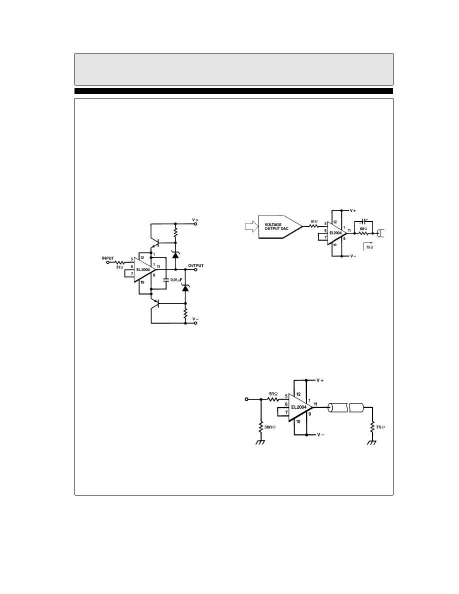
General Application Suggestions
Video DAC Buffer
Many of the available video D to A converters
are unable to directly drive 50
X or 75X cables.
The EL2004s excellent phase linearity at video
frequencies make it an ideal solution. In critical
applications or where line termination is not con-
trolled, a matching pad should be used as shown.
The capacitor should be adjusted for optimum
pulse response. If properly layed out this circuit
will not overshoot.
Video DAC Buffer
2004 - 14
Impedance Matching
The EL2004 provides power gain and isolation
between source and load when used as an active
tap or impedance matching device as illustrated
here. In this example, there is no output match-
ing pad between the 2004 and the 75
X line. Such
matching is not needed when the distant end of
the cable is properly terminated as there is no
reflected signal to worry about and the 2004 iso-
lates the source. This technique allows the full
output voltage of the EL2004 to be applied to the
load.
Impedance Converter
2004 - 15
9
EL2004/EL2004C
350 MHz FET Buffer
General Application Suggestions
à Contd.
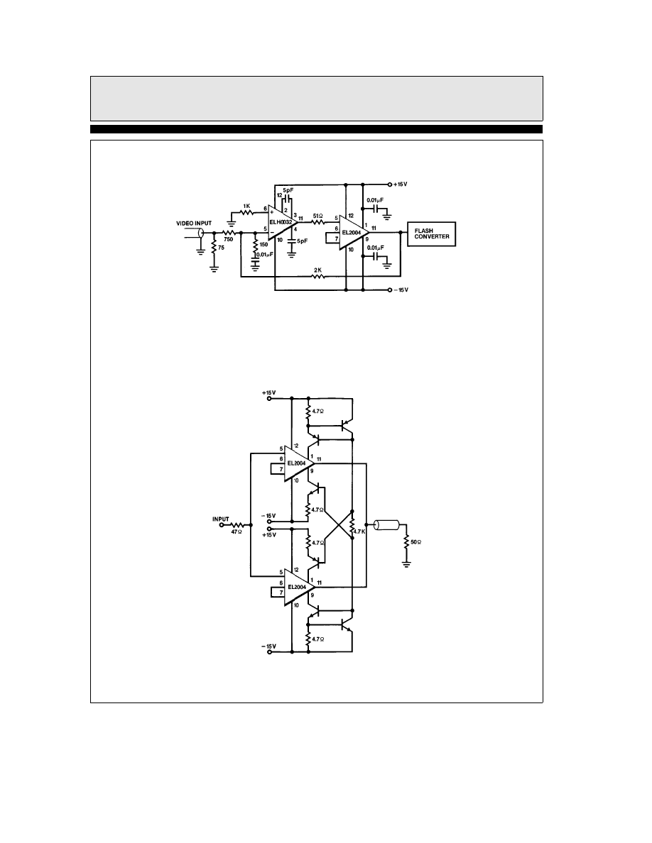
Inverting Amplifier for 20 MHz Flash Converter
2004 - 16
Boosting the Output
Unlike most integrated cicuits, two or more
EL2004s can be paralleled for increased output
drive. This capability results from the finite out-
put resistance and low output mismatch of the
EL2004. For example, a 50
X cable driver with
g
10V capability can be made by using two
EL2004s. A short-circuit protected version is
shown below.
50X Cable Driver with Short Circuit Protection
NPN
e
2N6551
(
PNP
e
2N6554
or equivalent
2W devices
2004 - 17
10
EL2004/EL2004C
350 MHz FET Buffer
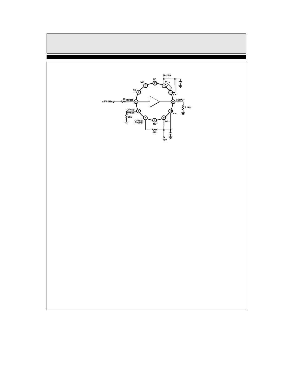
Burn-In Circuit
2004 - 18
Pin numbers are for TO-8 package.
LCC uses the same schematic.
11

EL2004/EL2004C
350 MHz FET Buffer
EL2004 Macromodel
* Connections:
input
*
l
V
a
*
l
l
Vc
a
*
l
l
l
V
b
*
l
l
l
l
Vc
b
*
l
l
l
l
l
output
*
l
l
l
l
l
l
.subckt M2004
5
12
1
10
9
11
* Models
.model qn npn (is
e
5e
b
14 bf
e
150 vaf
e
100 rc
e
1 rb
e
5 re
e
1 ikf
e
200mA
a
cje
e
5pF cjc
e
5pF mje
e
.42 mjc
e
.23 tf
e
.3nS tr
e
200nS br
e
5 vtf
e
0)
.model qp pnp (is
e
5e
b
14 bf
e
150 vaf
e
100 rc
e
2 rb
e
3 re
e
1 ikf
e
100mA
a
cje
e
5.7pF cjc
e
4pF tf
e
.3nS mje
e
.32 mjc
e
.43 tr
e
170nS br
e
5 vtf
e
0)
.model qf njf (vto
e b
3V beta
e
4.0e
b
3 cgd
e
4pF cgs
e
10pF lambda
e
671.0e
b
6)
* Resistors
r1 20 21 58.33
r2 27 10 58.33
r3 22 11 2
r4 11 23 2
* Transistors
j1 12 5 20 qf
j4 24 10 26 qf
q2 21 21 25 qn
q3 24 24 25 qp
q5 1 21 22 qn
q6 9 24 23 qp
q7 26 26 27 qn
.ends
12
TAB
WIDE
TD
is
3.8in

EL2004/EL2004C
350 MHz FET Buffer
EL2004 Macromodel
à Contd.
2004 - 19
13

BLANK
14

BLANK
15

EL2004/EL2004C
November
1993
Rev
G
EL2004/EL2004C
350 MHz FET Buffer
General Disclaimer
Specifications contained in this data sheet are in effect as of the publication date shown. Elantec, Inc. reserves the right to make changes
in the circuitry or specifications contained herein at any time without notice. Elantec, Inc. assumes no responsibility for the use of any
circuits described herein and makes no representations that they are free from patent infringement.
Elantec, Inc.
1996 Tarob Court
Milpitas, CA 95035
Telephone: (408) 945-1323
(800) 333-6314
Fax: (408) 945-9305
European Office: 44-71-482-4596
WARNING Ã Life Support Policy
Elantec, Inc. products are not authorized for and should not be
used within Life Support Systems without the specific written
consent of Elantec, Inc. Life Support systems are equipment in-
tended to support or sustain life and whose failure to perform
when properly used in accordance with instructions provided can
be reasonably expected to result in significant personal injury or
death. Users contemplating application of Elantec, Inc. products
in Life Support Systems are requested to contact Elantec, Inc.
factory headquarters to establish suitable terms & conditions for
these applications. Elantec, Inc.s warranty is limited to replace-
ment of defective components and does not cover injury to per-
sons or property or other consequential damages.
Printed in U.S.A.
16