| Secciones |
|---|
| Foros Electrónica |
|
|
| Boletines de correo |
 |
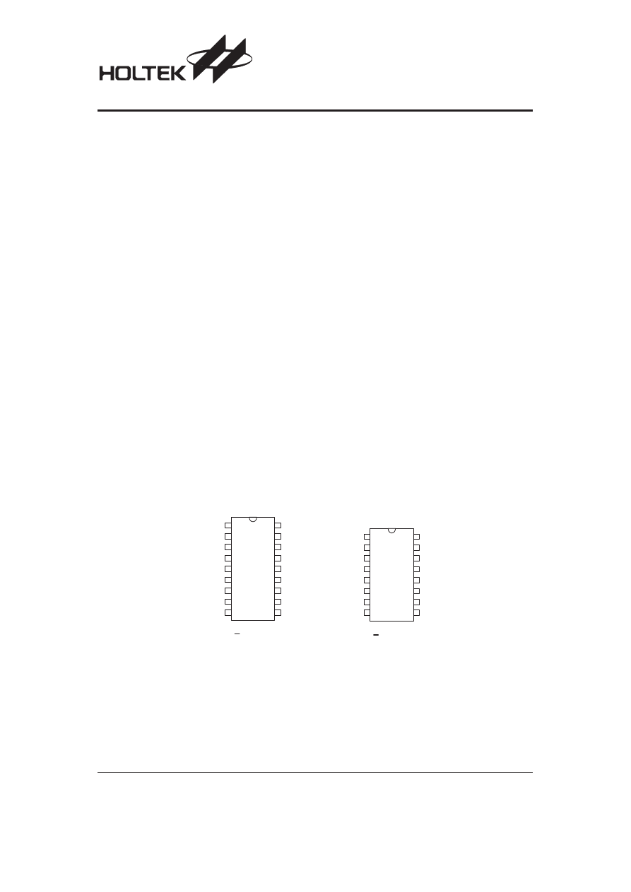
HT8950/HT8950A
Voice Modulator
Pin Assignment
Rev. 1.10
1
November 16, 2006
Features
·
Operating voltage: 2.4V~4.0V
·
On-chip SRAM
·
Robot function
·
Vibrato function
·
8kHz sampling rate
·
7-step level shifting
·
8-bit A/D and D/A converters
·
LED indicator with voice level
·
Push button selection or electronic mode
·
Minimal external components
·
HT8950: 18-pin DIP package
HT8950A: 16-pin DIP package
Applications
·
Educational Toys/leisure products
·
Mixers
·
Recorders
·
Audio system
·
Speech system
·
Telephone system
General Description
The HT8950/HT8950A are single chip CMOS LSI voice
modulator ICs which provide seven steps to shift the fre-
quency of an input voice, producing a dramatic change
in the output.
The HT8950/HT8950A provide two special effects: Vi-
brato and Robot. The Vibrato effect is generated by al-
ternating the frequency of an input signal up and down
at a rate of 8Hz. The Robot function, on the other hand,
converts an input voice into a Robot voice. Both effects
can be selected depending on which pin is triggered, ei-
ther ROB or VIB. For the output frequency level shifting,
the chips provide seven steps which can be selected
from the two groups of pins namely, SW0, SW1 and
SW2 for electronic direct selection and ROB, TGD, TGU
and VIB for push button selection.
The HT8950/HT8950A include a built-in microphone
amplifier with an internal bias, an 8-bit A/D converter, a
built-in SRAM as well as a current output type 8-bit D/A
converter. The 8-bit A/D and D/A converters with a sam-
pling rate of 8kHz ensures a high quality and high S/N
ratio output voice. The chips provide an LED indicator
which flashes in accordance with the volume of the input
voices.
1 6
1 5
1 4
1 3
1 2
1 1
1 0
9
1
2
3
4
5
6
7
8
O S C 2
F V I B
T S
V R E F
A U D I O
L A M P
V D D
A I N
O S C 1
V I B
T G U
T G D
R O B
V S S
N C
A O
1 8
1 7
1 6
1 5
1 4
1 3
1 2
1 1
1 0
1
2
3
4
5
6
7
8
9
R O B
T G D
T G U
V I B
O S C 1
O S C 2
F V I B
T S
V R E F
S W 0
S W 1
S W 2
V S S
A O
A I N
V D D
L A M P
A U D I O
H T 8 9 5 0
1 8 D I P - A
H T 8 9 5 0 A
1 6 D I P - A
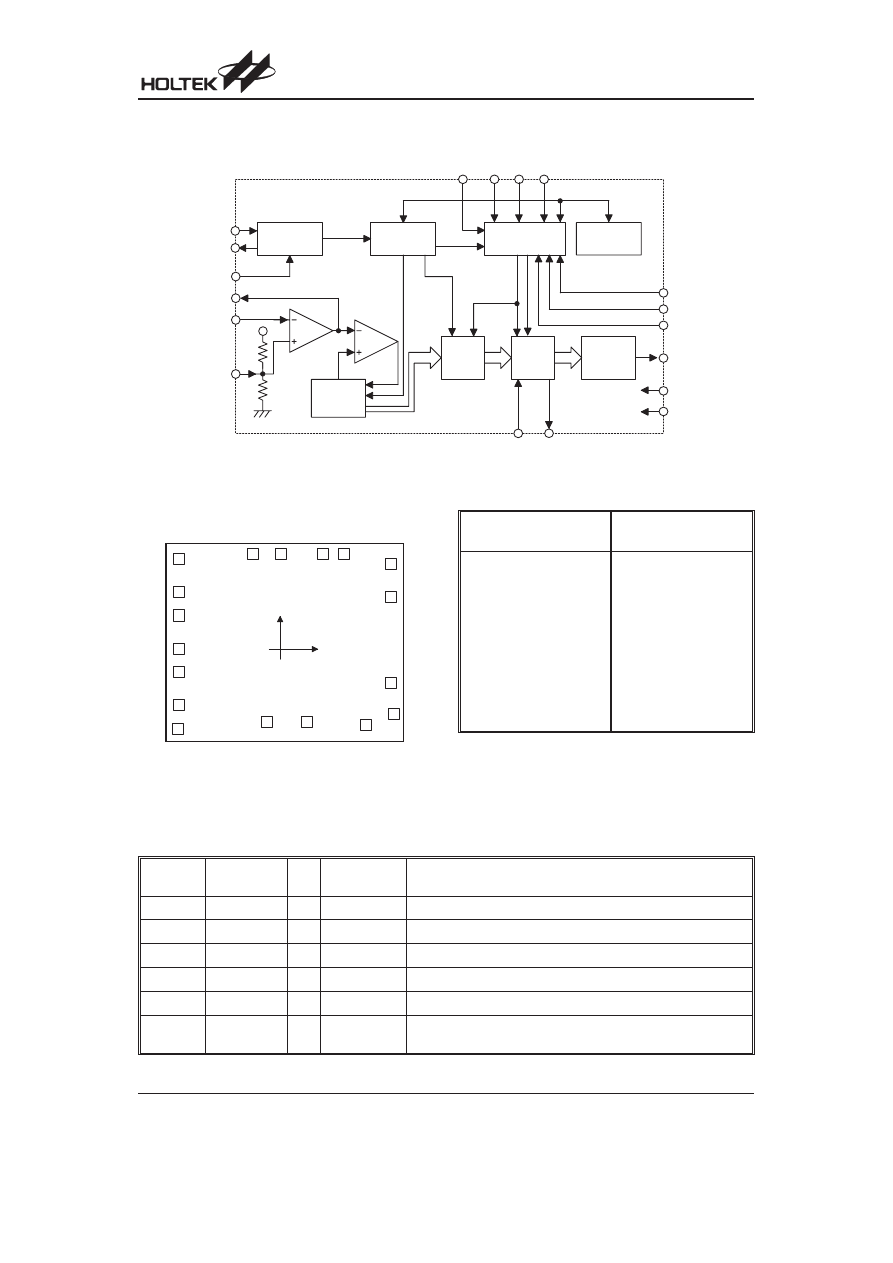
Block Diagram
Pad Coordinates
Unit:
mm
Pad
No.
X
Y
Pad
No.
X
Y
1
-957.0
720.5
10
732.0
-774.0
2
-957.0
423.5
11
984.0
-675.0
3
-957.0
210.0
12
956.5
-400.0
4
-957.0
-87.0
13
956.5
374.5
5
-957.0
-299.5
14
956.5
671.5
6
-957.0
-596.5
15
530.5
765.5
7
-962.0
-815.0
16
345.50
765.5
8
-161.5
-747.5
17
-33.50
765.5
9
200.5
-747.5
18
-287.50
765.5
Chip size: 2350
´2080 (mm)
2
The IC substrate should be connected to VSS in the PCB layout artwork.
Pin Description (HT8950)
Pin No.
Pin Name
I/O
Internal
Connection
Description
1~3
SW0~SW2
I
Pull-High
Function setting pin (for electronic setting)
4
VSS
I
¾
Negative power supply, ground
5
AO
O
¾
Internal amplifier output
6
AIN
I
¾
Internal amplifier input (inverted)
7
VDD
O
¾
Positive power supply
8
LAMP
O
NMOS
Open Drain
Lamp output (the brightness changes with the voice volume)
HT8950/HT8950A
Rev. 1.10
2
November 16, 2006
O s c i l l a t o r
G e n e r a t o r
T i m e B a s e
G e n e r a t o r
C o n t r o l
C i r c u i t
P o w e r O n
C i r c u i t
A / D
C o n v e r t e r
D / A
C o n v e r t e r
S R A M
L a t c h
T G U
T G D V I B R O B
S W 0
S W 1
S W 2
A U D I O
V S S
V D D
O S C 2
F V I B
A O
A I N
V R E F
T S
L A M P
O S C 1
1
1 0
2
1 1
3
1 2
4
1 3
5
1 4
6
1 5
7
1 6
8
1 7
9
1 8
( 0 , 0 )
T G U
V S S
A
O
A
IN
V
D
D
V
IB
A U D I O
L A M P
O
S
C
1
O
S
C
2
FV
IB
T G D
R O B
S W 0
S W 1
S W 2
T S
V R E F
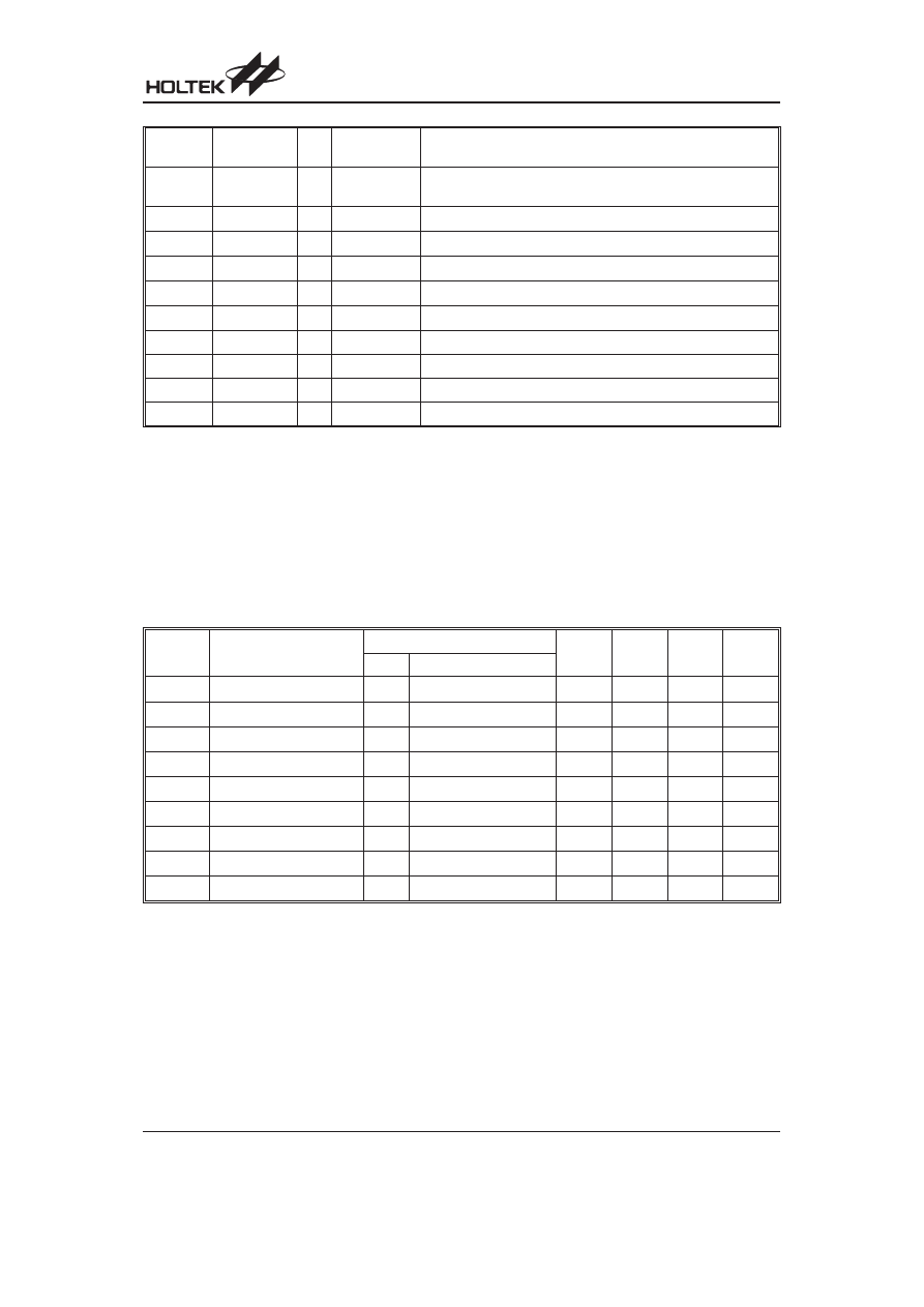
Pin No.
Pin Name
I/O
Internal
Connection
Description
9
AUDIO
O
PMOS
Open Drain
Audio output
10
VREF
I
¾
Internal amplifier reference voltage
11
TS
I
¾
For IC test only
12
FVIB
O
¾
Vibrato frequency control
13
OSC2
O
¾
Oscillator output
14
OSC1
I
¾
Oscillator input
15
VIB
I
Pull-High
Switch to Vibrato mode (toggle)
16
TGU
I
Pull-High
Switch to Upward step mode
17
TGD
I
Pull-High
Switch to Downward step mode (internal pull-high)
18
ROB
I
Pull-High
Switch to Robot mode (internal pull-high)
Absolute Maximum Ratings
Supply Voltage ...........................V
SS
-0.3V to V
SS
+4.5V
Storage Temperature ............................
-50 °C to 125 °C
Input Voltage..............................V
SS
-0.3V to V
DD
+0.3V
Operating Temperature...........................
-20 °C to 70 C
Note: These are stress ratings only. Stresses exceeding the range specified under
²Absolute Maximum Ratings ² may
cause substantial damage to the device. Functional operation of this device at other conditions beyond those listed
in the specification is not implied and prolonged exposure to extreme conditions may affect device reliability.
Electrical Characteristics
Ta=25
°C
Symbol
Parameter
Test Conditions
Min.
Typ.
Max.
Unit
V
DD
Conditions
V
DD
Operating Voltage
¾
¾
2.4
3.0
4.0
V
I
OP
Operating Current
3V
No load, f
OSC
=640kHz
¾
2.0
10
mA
V
IN
Input Signal
3V
¾
¾
¾
580
mV
I
LAMP
Lamp Sink Current
3V
V
OL
=1.3V
5.0
9.5
¾
mA
A
V
OPA Gain Value
3V
Open loop
¾
2000
¾
I
O
Audio Output Voltage
3V
During silence
¾
-1
¾
mA
V
IH
High Input Voltage
¾
¾
0.7V
DD
¾
¾
V
V
IL
Low Input Voltage
¾
¾
¾
¾
0.3V
DD
V
f
OSC
Oscillating Frequency
3V
R
OSC
=47k
W
¾
512
¾
kHz
HT8950/HT8950A
Rev. 1.10
3
November 16, 2006
HT8950/HT8950A
Rev. 1.10
4
November 16, 2006
Functional Description
The HT8950/HT8950A are single chip LSIs designed for
voice modulation. These devices provide seven steps to
shift the frequency of an input voice signal up and down.
The chips are also equipped with two special effects; Vi-
brato and Robot.
The HT8950/HT8950A include a built-in amplifier, 8-bit
A/D converter and current output type of 8-bit D/A con-
verter in addition to a built-in SRAM. The brightness of
the LED indicator changes with the volume of the input
voice signal.
Power on Initial
The HT8950/HT8950A enter the Robot state right after
power is initially switched on.
Robot State
The system goes into the Robot state after the ROB pin
is triggered or power is turned on. In this mode, an input
voice can be converted into a robot voice.
Vibrato
An output voice will be generated with a vibrato effect
when the VIB pin is triggered, regardless of what state
the system is in. The vibrato effect is toggle activated. In
other words, when a voice output is playing with a vi-
brato effect, this effect can be eliminated by retriggering
the VIB pin. The rate of vibrato effect can be changed by
adjusting the resistance of the external resistor between
the OSC2 and FVIB pins.
Voice Modulation
The HT8950/HT8950A provide an 8-bit A/D and D/A
converters with a sampling rate of 8kHz, ensuring a high
quality voice output and with a high S/N ratio. The chips
include seven steps to shift the frequency of an input
signal. The voice modulation is selected and deter-
mined by the SW0~SW2 inputs.
Input
Step Mode
Speed
Ratio
SW2
SW1
SW0
1
1
1
Controlled by TGU and
TDG
Notes
1
1
0
UP3
2
1
0
1
UP2
8/5
1
0
0
UP1
4/3
0
1
1
NORMAL
1
0
1
0
DN1
8/9
0
0
1
DN2
4/5
0
0
0
DN3
2/3
Notes: The TGU switch increments by one step mode,
and the TGD switch, on the other hand, decrements by
one step mode, step by step as shown:
·
The system changes to the Robot state after the ROB
pin is triggered, regardless of what state the system is
in.
·
A voice output is accompanied with a vibrato effect af-
ter the VIB pin is triggered, regardless of what state
the system is in.
LED Indicator
The HT8950/HT8950A provide a LAMP pin to drive an
external LED. The brightness of the LED changes with
the volume of the input voice signal.
*
R O B O T
T G U
T G D
D N 3
T G U
T G D
D N 2
T G U
T G D
D N 1
T G U
T G D
N O R M A L
T G U
T G D
U P 1
T G U
T G D
U P 2
T G U
T G D
U P 3
T G U
T G D
Application Circuits
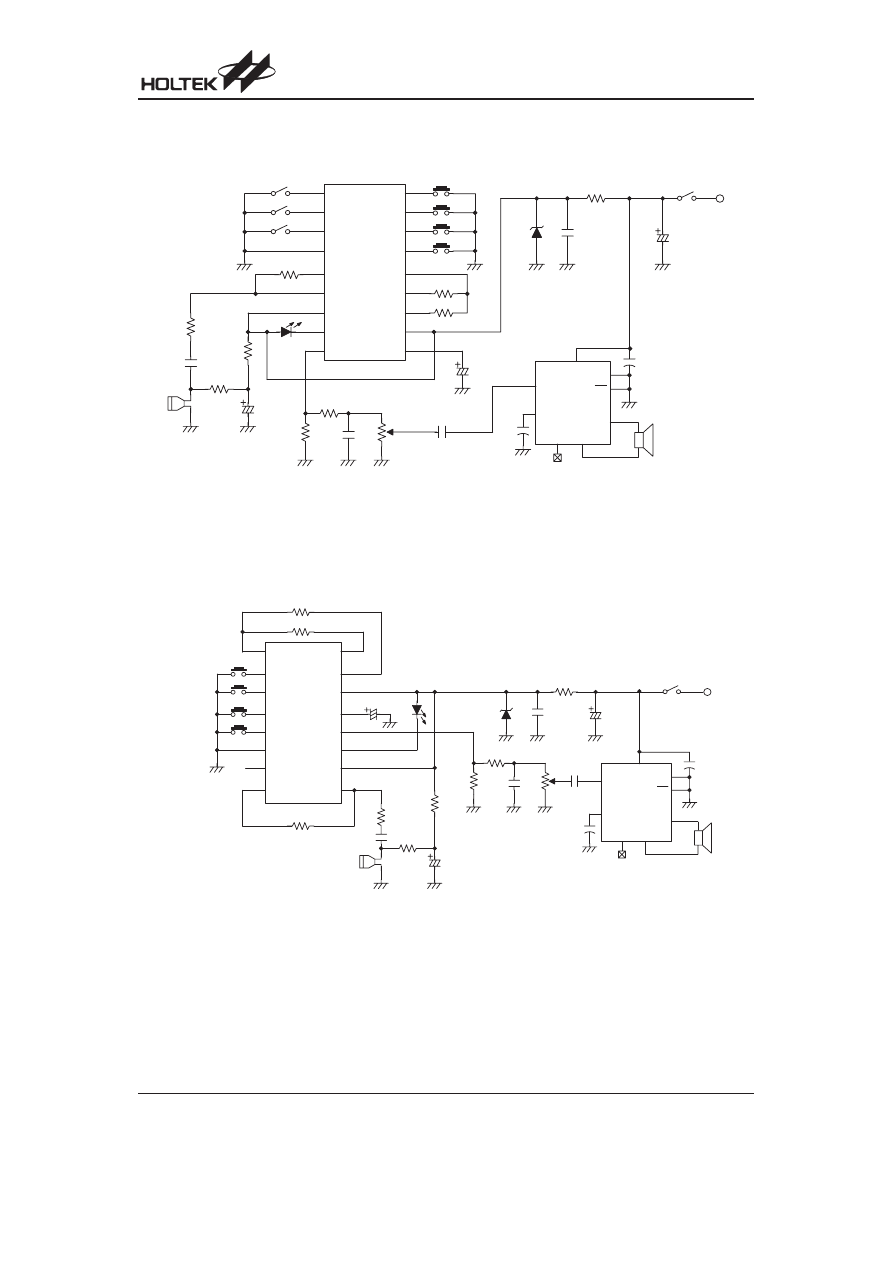
HT8950 with HT82V733 Power Amplifier and a 6V Power Supply
HT8950A with HT82V733 Power Amplifier and a 6V Power Supply
HT8950/HT8950A
Rev. 1.10
5
November 16, 2006
9
1 0
1 1
1 2
1 3
1 4
1 5
1 6
1
3
5
2
4
6
8
7
O S C 1
O S C 2
V S S
N C
A O
A U D I O
F V I B
V R E F
V D D
A I N
L A M P
R O B
V I B
T G D
T G U
T S
4 . 7 m F / 1 0 V
3 . 6 V
1 0 0 m F /
1 0 V
V C C
4 . 5 V
0 . 1 m F
4 7 0 W
4 . 7 k W
3 3 k W
4 . 7 k W
0 . 1 m F
2 2 m F / 1 0 V
M I C
1 0 0 k W
4 7 k W
H T 8 9 5 0 A
3 3 0 W
0 . 1 m F
1
2
3
4
5
6
7
8
H T 8 2 V 7 3 3
4 7 m F
1 m F
O U T N
V D D
V R E F
C E
N C
O U T P
A u d i o I n
S P K
V S S
0 . 0 3 3 m F
5 1 0 W
5 0 k W
3 3 k W
4 . 7 m F / 1 0 V
3 . 6 V
1 0 0 k W
4 7 k W
0 . 1 m F
4 7 0 W
1 0 0 m F / 1 0 V
V C C
4 . 5 V
1
3
5
2
4
6
8
7
4 7 0 W
4 . 7 k W
4 . 7 k W
0 . 1 m F
2 2 m F / 1 0 V
M I C
3 3 k W
9
1 0
1 1
1 2
1 3
1 4
1 5
1 6
O S C 1
O S C 2
V S S
A O
A U D I O
F V I B
V R E F
V D D
A I N
L A M P
R O B
V I B
T G D
T G U
T S
1 7
1 8
S W 0
S W 1
S W 2
H T 8 9 5 0
0 . 1 m F
1
2
3
4
5
6
7
8
H T 8 2 V 7 3 3
4 7 m F
1 m F
O U T N
V D D
V R E F
C E
N C
O U T P
A u d i o I n
S P K
V S S
0 . 0 3 3 m F
5 1 0 W
5 0 k W
3 3 k W
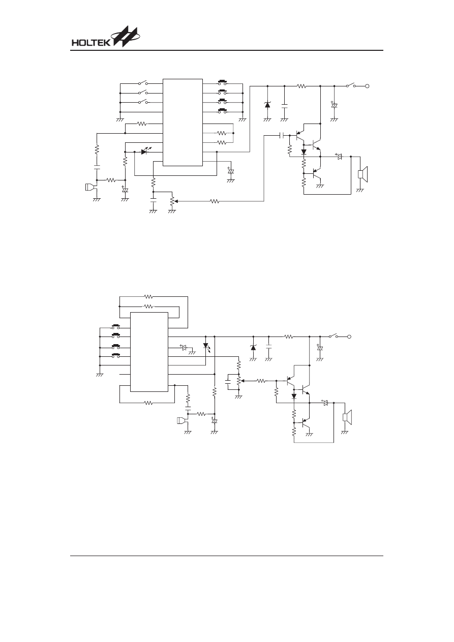
HT8950 with a Transistor Output Stage and a 6V Power Supply
HT8950A with a Transistor Output Stage and a 6V Power Supply
HT8950/HT8950A
Rev. 1.10
6
November 16, 2006
9
1 0
1 1
1 2
1 3
1 4
1 5
1 6
1
3
5
2
4
6
8
7
O S C 1
O S C 2
V S S
N C
A O
A U D I O
F V I B
V R E F
V D D
A I N
L A M P
R O B
V I B
T G D
T G U
T S
4 . 7 m F / 1 0 V
3 . 6 V
0 . 1 m F
4 7 0 W
1 0 0 m F / 1 0 V
V C C
6 V
2 0 0 W
2 . 4 k W
1 0 0 m F / 1 0 V
S P K
0 . 1 m F
4 7 0 W
4 . 7 k W
3 3 k W
0 . 1 m F
2 2 m F / 1 0 V
M I C
3 3 0 W
H T 8 9 5 0 A
1 5 0 k W
A 7 3 3
8 0 5 0
6 8 W
4 7 0 W
8 0 5 0
4 . 7 k W
1 0 0 k W
4 7 k W
4 . 7 m F / 1 0 V
3 . 6 V
1 0 0 k W
4 7 k W
1 0 0 m F / 1 0 V
V C C
6 V
0 . 1 m F
1
3
5
2
4
6
8
7
4 7 0 W
4 . 7 k W
4 . 7 k W
0 . 1 m F
2 2 m F / 1 0 V
M I C
2 . 4 k W
2 0 0 W
0 . 1 m F
3 3 0 W
3 3 k W
9
1 0
1 1
1 2
1 3
1 4
1 5
1 6
O S C 1
O S C 2
V S S
A O
A U D I O
F V I B
V R E F
V D D
A I N
L A M P
R O B
V I B
T G D
T G U
T S
1 7
1 8
S W 0
S W 1
S W 2
1 0 0 m F / 1 0 V
S P K
H T 8 9 5 0
A 7 3 3
8 0 5 0
1 5 0 W
8 0 5 0
6 8 W
4 7 0 W
0 . 1 m F
4 7 0 W
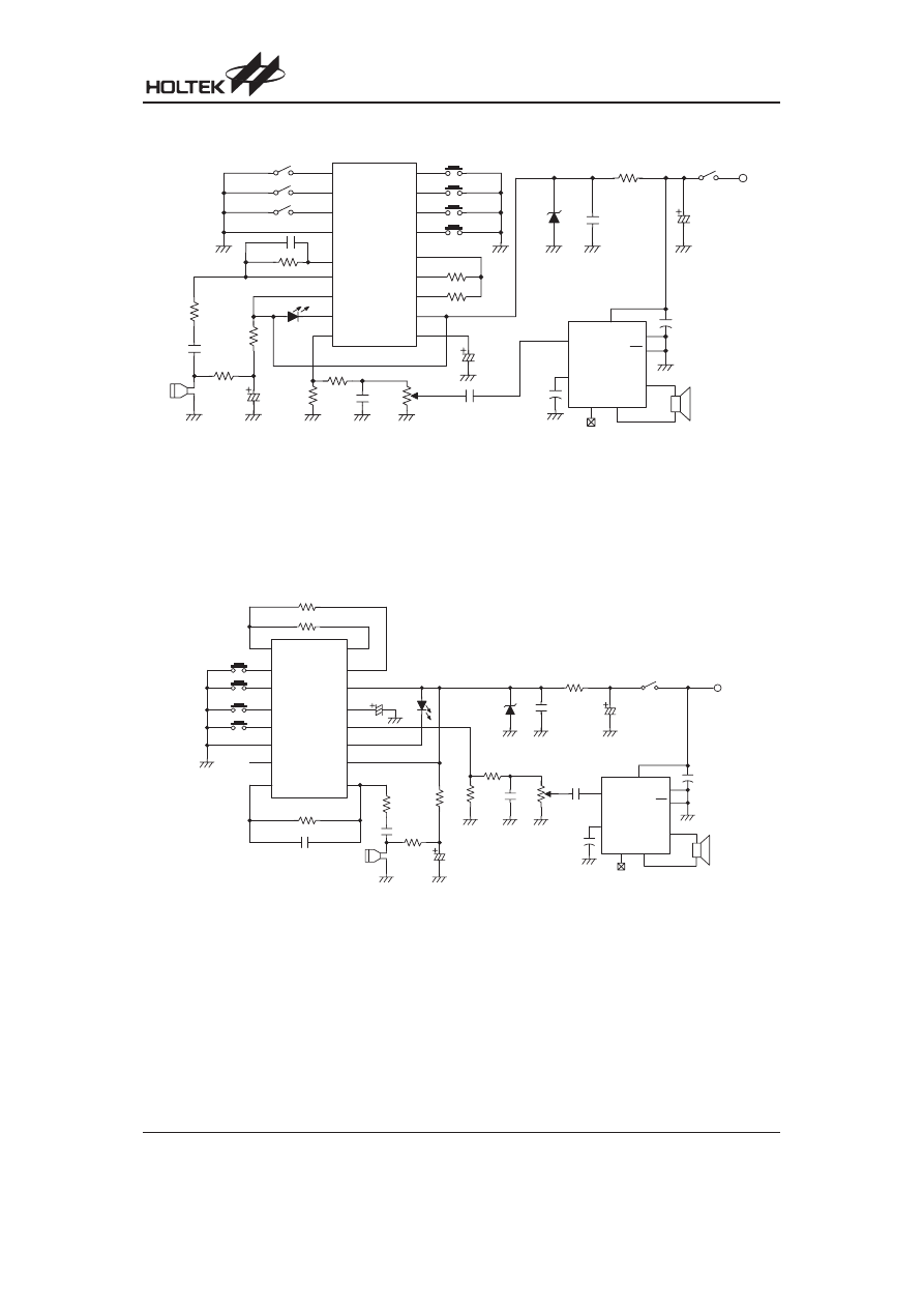
HT8950 with HT82V733 Power Amplifier and a 6V Power Supply
HT8950A with HT82V733 Power Amplifier and a 6V Power Supply
HT8950/HT8950A
Rev. 1.10
7
November 16, 2006
9
1 0
1 1
1 2
1 3
1 4
1 5
1 6
1
3
5
2
4
6
8
7
O S C 1
O S C 2
V S S
N C
A O
A U D I O
F V I B
V R E F
V D D
A I N
L A M P
R O B
V I B
T G D
T G U
T S
4 . 7 m F / 1 0 V
3 . 6 V
1 0 0 m F / 1 0 V
V C C
4 . 5 V
0 . 0 3 3 m F
3 9 k W
0 . 1 m F
2 2 m F / 1 0 V
M I C
H T 8 9 5 0 A
0 . 0 4 7 m F
4 7 k W
4 . 7 k W
4 7 0 W
5 1 0 W
3 3 k W
5 0 k W
4 7 0 W
0 . 1 m F
1 0 0 k W
4 7 k W
0 . 1 m F
1
2
3
4
5
6
7
8
H T 8 2 V 7 3 3
4 7 m F
1 m F
O U T N
V D D
V R E F
C E
N C
O U T P
A u d i o I n
S P K
V S S
4 . 7 m F /
1 0 V
3 . 6 V
0 . 1 m F
1 0 0 m F / 1 0 V
V C C
4 . 5 V
1
3
5
2
4
6
8
7
4 . 7 k W
0 . 1 m F
2 2 m F / 1 0 V
M I C
0 . 0 3 3 m F
9
1 0
1 1
1 2
1 3
1 4
1 5
1 6
O S C 1
O S C 2
V S S
A O
A U D I O
F V I B
V R E F
V D D
A I N
L A M P B
R O B
V I B
T G D
T G U
T S
1 7
1 8
S W 0
S W 1
S W 2
H T 8 9 5 0
0 . 1 m F
0 . 0 4 7 m F
4 . 7 k W
4 7 0 W
3 9 k W
5 1 0 W
3 3 k W
5 0 k W
1 0 0 k W
4 7 k W
4 7 0 W
1
2
3
4
5
6
7
8
H T 8 2 V 7 3 3
4 7 m F
1 m F
O U T N
V D D
V R E F
C E
N C
O U T P
A u d i o I n
S P K
V S S

Package Information
16-pin DIP (300mil) Outline Dimensions
Symbol
Dimensions in mil
Min.
Nom.
Max.
A
745
¾
775
B
240
¾
260
C
125
¾
135
D
125
¾
145
E
16
¾
20
F
50
¾
70
G
¾
100
¾
H
295
¾
315
I
335
¾
375
a
0
°
¾
15
°
HT8950/HT8950A
Rev. 1.10
8
November 16, 2006
a
1 6
1
9
8
A
B
C
D
E
F
G
H
I
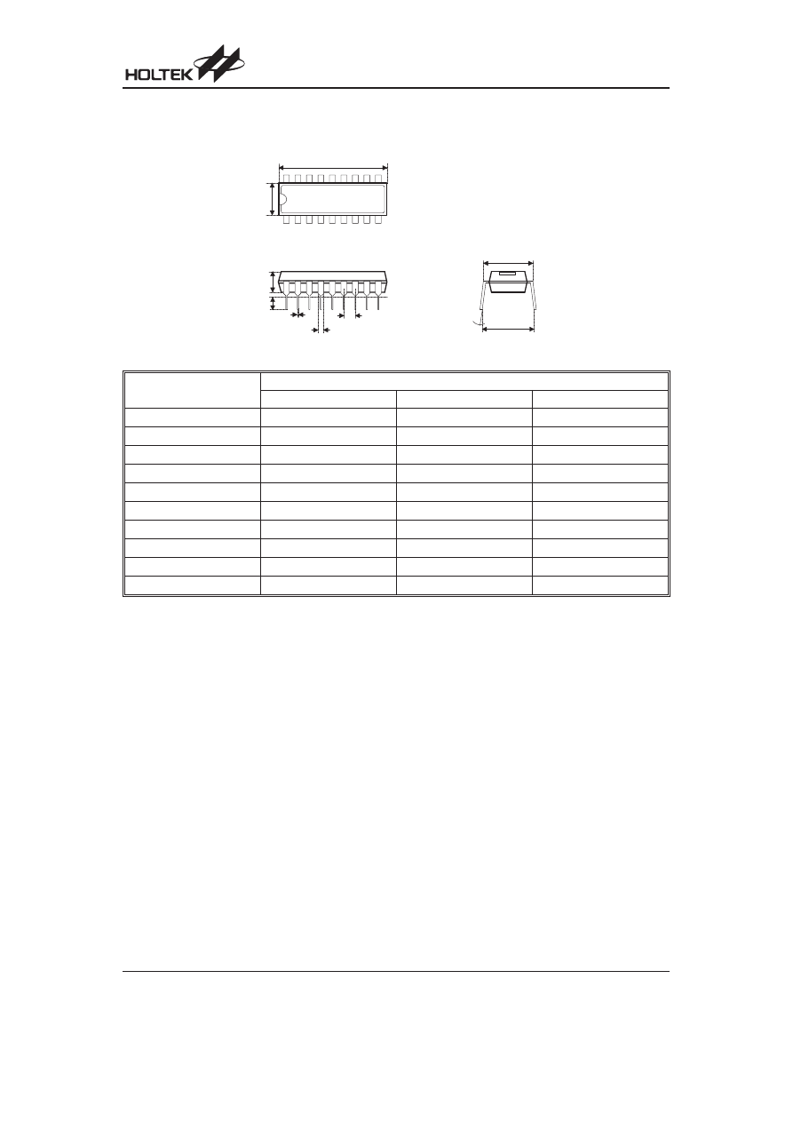
18-pin DIP (300mil) Outline Dimensions
Symbol
Dimensions in mil
Min.
Nom.
Max.
A
895
¾
915
B
240
¾
260
C
125
¾
135
D
125
¾
145
E
16
¾
20
F
50
¾
70
G
¾
100
¾
H
295
¾
315
I
335
¾
375
a
0
°
¾
15
°
HT8950/HT8950A
Rev. 1.10
9
November 16, 2006
1 8
1
1 0
9
a
A
B
C
D
E
F
G
H
I

HT8950/HT8950A
Rev. 1.10
10
November 16, 2006
Holtek Semiconductor Inc. (Headquarters)
No.3, Creation Rd. II, Science Park, Hsinchu, Taiwan
Tel: 886-3-563-1999
Fax: 886-3-563-1189
http://www.holtek.com.tw
Holtek Semiconductor Inc. (Taipei Sales Office)
4F-2, No. 3-2, YuanQu St., Nankang Software Park, Taipei 115, Taiwan
Tel: 886-2-2655-7070
Fax: 886-2-2655-7373
Fax: 886-2-2655-7383 (International sales hotline)
Holtek Semiconductor Inc. (Shanghai Sales Office)
7th Floor, Building 2, No.889, Yi Shan Rd., Shanghai, China 200233
Tel: 86-21-6485-5560
Fax: 86-21-6485-0313
http://www.holtek.com.cn
Holtek Semiconductor Inc. (Shenzhen Sales Office)
5/F, Unit A, Productivity Building, Cross of Science M 3rd Road and Gaoxin M 2nd Road, Science Park, Nanshan District,
Shenzhen, China 518057
Tel: 86-755-8616-9908, 86-755-8616-9308
Fax: 86-755-8616-9533
Holtek Semiconductor Inc. (Beijing Sales Office)
Suite 1721, Jinyu Tower, A129 West Xuan Wu Men Street, Xicheng District, Beijing, China 100031
Tel: 86-10-6641-0030, 86-10-6641-7751, 86-10-6641-7752
Fax: 86-10-6641-0125
Holtek Semiconductor Inc. (Chengdu Sales Office)
709, Building 3, Champagne Plaza, No.97 Dongda Street, Chengdu, Sichuan, China 610016
Tel: 86-28-6653-6590
Fax: 86-28-6653-6591
Holmate Semiconductor, Inc. (North America Sales Office)
46729 Fremont Blvd., Fremont, CA 94538
Tel: 1-510-252-9880
Fax: 1-510-252-9885
http://www.holmate.com
Copyright
2006 by HOLTEK SEMICONDUCTOR INC.
The information appearing in this Data Sheet is believed to be accurate at the time of publication. However, Holtek as-
sumes no responsibility arising from the use of the specifications described. The applications mentioned herein are used
solely for the purpose of illustration and Holtek makes no warranty or representation that such applications will be suitable
without further modification, nor recommends the use of its products for application that may present a risk to human life
due to malfunction or otherwise. Holtek s products are not authorized for use as critical components in life support devices
or systems. Holtek reserves the right to alter its products without prior notification. For the most up-to-date information,
please visit our web site at http://www.holtek.com.tw.
Document Outline

