| Secciones |
|---|
| Foros Electrónica |
|
|
| Boletines de correo |
 |

LF351
LF351 Wide Bandwidth JFET Input Operational Amplifier
Literature Number: SNOSBH2
LF351
Wide Bandwidth JFET Input Operational Amplifier
General Description
The LF351 is a low cost high speed JFET input operational
amplifier with an internally trimmed input offset voltage
(BI-FET II
™
technology). The device requires a low supply
current and yet maintains a large gain bandwidth product
and a fast slew rate. In addition, well matched high voltage
JFET input devices provide very low input bias and offset
currents. The LF351 is pin compatible with the standard
LM741 and uses the same offset voltage adjustment cir-
cuitry. This feature allows designers to immediately upgrade
the overall performance of existing LM741 designs.
The LF351 may be used in applications such as high speed
integrators, fast D/A converters, sample-and-hold circuits
and many other circuits requiring low input offset voltage,
low input bias current, high input impedance, high slew rate
and wide bandwidth. The device has low noise and offset
voltage drift, but for applications where these requirements
are critical, the LF356 is recommended. If maximum supply
current is important, however, the LF351 is the better choice.
Features
n
Internally trimmed offset voltage:
10 mV
n
Low input bias current:
50 pA
n
Low input noise voltage:
n
Low input noise current:
n
Wide gain bandwidth:
4 MHz
n
High slew rate:
13 V/ µs
n
Low supply current:
1.8 mA
n
High input impedance:
10
12
Ω¦
n
Low total harmonic distortion A
V
=10,:
<
0.02%
R
L
=10k, V
O
=20 Vp-p, BW=20 Hz-20 kHz
n
Low 1/f noise corner:
50 Hz
n
Fast settling time to 0.01%:
2 µs
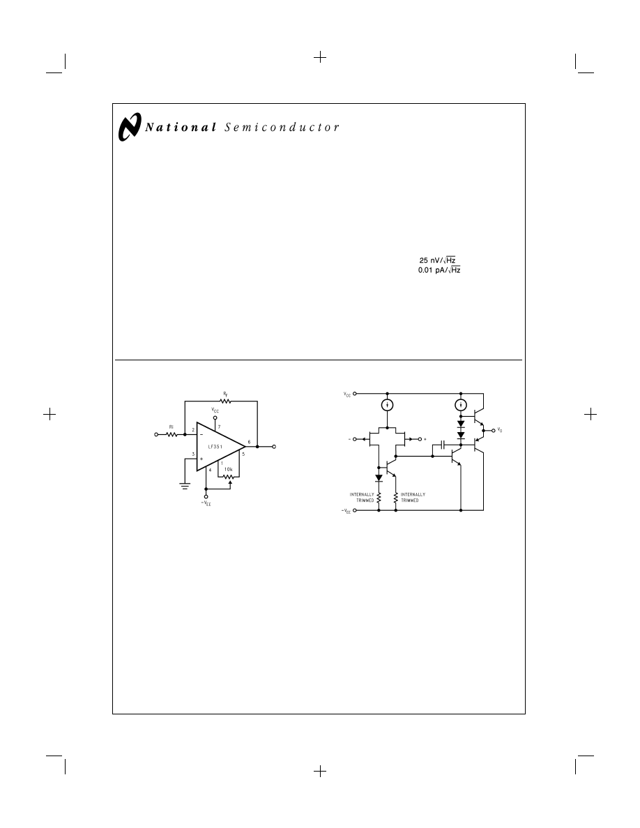
Typical Connection
Simplified Schematic
BI-FET II
™
is a trademark of National Semiconductor Corporation.
DS005648-11
DS005648-12
April 1998
LF351
W
ide
Bandwidth
JFET
Input
Operational
Amplifier
LF351
© 1998 National Semiconductor Corporation
DS005648
www.national.com
1
PrintDate=1998/04/07 PrintTime=13:52:34 38265 ds005648 Rev. No. 3
cmserv
Proof
1
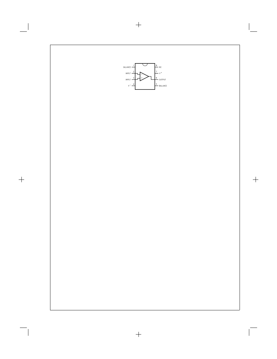
Connection Diagram
Dual-In-Line Package
DS005648-13
Order Number LF351M or LF351N
See NS Package Number M08A or N08E
PrintDate=1998/04/07 PrintTime=13:52:34 38265 ds005648 Rev. No. 3
cmserv
Proof
2
www.national.com
2
Absolute Maximum Ratings
(Note 1)
If Military/Aerospace specified devices are required,
please contact the National Semiconductor Sales Office/
Distributors for availability and specifications.
Supply Voltage
±
18V
Power Dissipation (Notes 2, 7)
670 mW
Operating Temperature Range
0°C to +70°C
T
j(MAX)
115°C
Differential Input Voltage
±
30V
Input Voltage Range (Note 3)
±
15V
Output Short Circuit Duration
Continuous
Storage Temperature Range
-65°C to +150°C
Lead Temp. (Soldering, 10 sec.)
Metal Can
300°C
DIP
260°C
Θ
jA
N Package
120°C/W
M Package
TBD
Soldering Information
Dual-In-Line Package
Soldering (10 sec.)
260°C
Small Outline Package
Vapor Phase (60 sec.)
215°C
Infrared (15 sec.)
220°C
See AN-450 Surface Mounting Methods and Their Effect on
Product Reliability for other methods of soldering surface
mount devices.
ESD rating to be determined
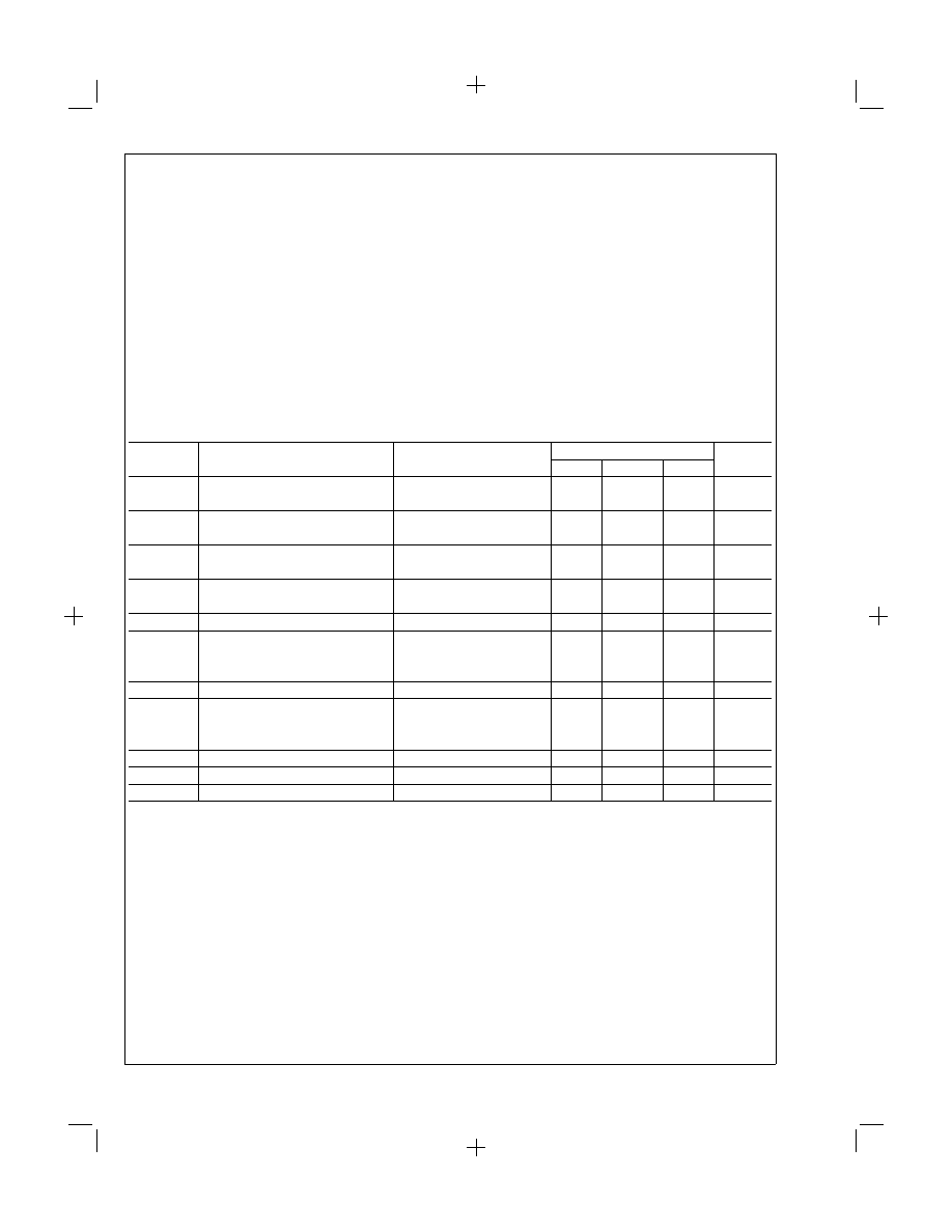
DC Electrical Characteristics
(Note 4)
Symbol
Parameter
Conditions
LF351
Units
Min
Typ
Max
V
OS
Input Offset Voltage
R
S
= 10 k
Ω¦
, T
A
= 25°C
5
10
mV
Over Temperature
13
mV
∆
V
OS
/
∆
T
Average TC of Input Offset
R
S
=10 k
Ω¦
10
µV/°C
Voltage
I
OS
Input Offset Current
T
j
= 25°C, (Notes 4, 5)
25
100
pA
T
j
≤
70°C
4
nA
I
B
Input Bias Current
T
j
= 25°C, (Notes 4, 5)
50
200
pA
T
j
≤
±
70°C
8
nA
R
IN
Input Resistance
T
j
=25°C
10
12
Ω¦
A
VOL
Large Signal Voltage Gain
V
S
=
±
15V, T
A
=25°C
25
100
V/mV
V
O
=
±
10V, R
L
=2 k
Ω¦
Over Temperature
15
V/mV
V
O
Output Voltage Swing
V
S
=
±
15V, R
L
=10 k
Ω¦
±
12
±
13.5
V
V
CM
Input Common-Mode Voltage
+15
V
Range
V
S
=
±
15V
±
11
-12
V
CMRR
Common-Mode Rejection Ratio
R
S
≤
10 k
Ω¦
70
100
dB
PSRR
Supply Voltage Rejection Ratio
(Note 6)
70
100
dB
I
S
Supply Current
1.8
3.4
mA
Note 1: Absolute Maximum Ratings indicate limits beyond which damage to the device may occur. Operating Ratings indicate conditions for which the device is func-
tional, but do not guarantee specific performance limits.
Note 2: For operating at elevated temperature, the device must be derated based on the thermal resistance,
Θ
JA
.
Note 3: Unless otherwise specified the absolute maximum negative input voltage is equal to the negative power supply voltage.
Note 4: These specifications apply for V
S
=
±
15V and 0°C
≤
T
A
≤
+70°C. V
OS
, I
B
and I
OS
are measured at V
CM
=0.
Note 5: The input bias currents are junction leakage currents which approximately double for every 10°C increase in the junction temperature, T
j
. Due to the limited
production test time, the input bias currents measured are correlated to junction temperature. In normal operation the junction temperature rises above the ambient
temperature as a result of internal power dissipation, P
D
. T
j
=T
A
+
Θ
jA
P
D
where
Θ
jA
is the thermal resistance from junction to ambient. Use of a heat sink is recom-
mended if input bias current is to be kept to a minimum.
Note 6: Supply voltage rejection ratio is measured for both supply magnitudes increasing or decreasing simultaneously in accordance with common practice. From
±
15V to
±
5V.
Note 7: Max. Power Dissipation is defined by the package characteristics. Operating the part near the Max. Power Dissipation may cause the part to operate outside
guaranteed limits.
3
www.national.com
PrintDate=1998/04/07 PrintTime=13:52:34 38265 ds005648 Rev. No. 3
cmserv
Proof
3
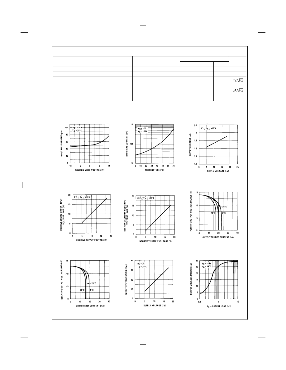
AC Electrical Characteristics
(Note 4)
Symbol
Parameter
Conditions
LF351
Units
Min
Typ
Max
SR
Slew Rate
V
S
=
±
15V, T
A
=25°C
13
V/ µs
GBW
Gain Bandwidth Product
V
S
=
±
15V, T
A
=25°C
4
MHz
e
n
Equivalent Input Noise Voltage
T
A
= 25°C, R
S
=100
Ω¦
,
25
f = 1000 Hz
i
n
Equivalent Input Noise Current
T
j
= 25°C, f=1000 Hz
0.01
Typical Performance Characteristics
Input Bias Current
DS005648-14
Input Bias Current
DS005648-15
Supply Current
DS005648-16
Positive Common-Mode
Input Voltage Limit
DS005648-17
Negative Common-Mode
Input Voltage Limit
DS005648-18
Positive Current Limit
DS005648-19
Negative Current Limit
DS005648-20
Voltage Swing
DS005648-21
Output Voltage Swing
DS005648-22
PrintDate=1998/04/07 PrintTime=13:52:34 38265 ds005648 Rev. No. 3
cmserv
Proof
4
www.national.com
4
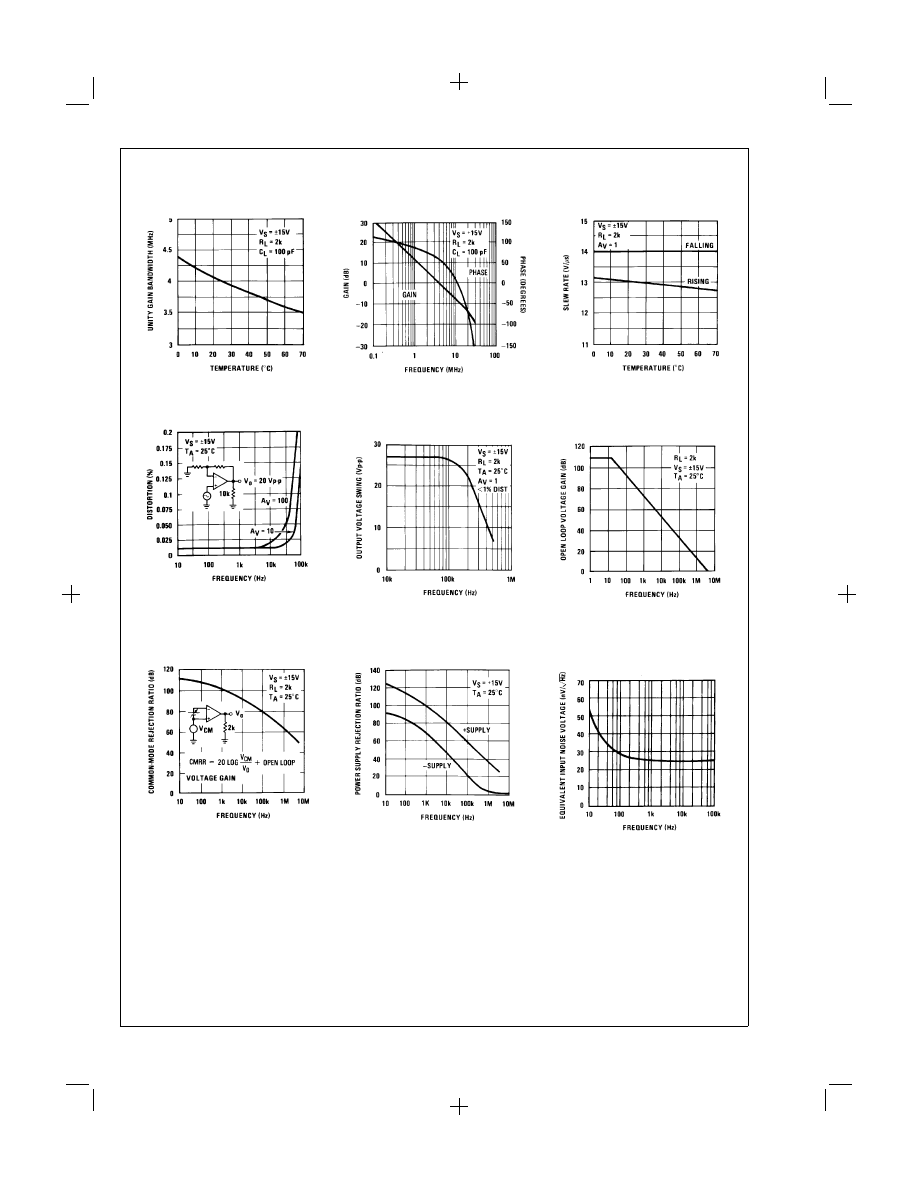
Typical Performance Characteristics
(Continued)
Gain Bandwidth
DS005648-23
Bode Plot
DS005648-24
Slew Rate
DS005648-25
Distortion vs Frequency
DS005648-26
Undistorted Output
Voltage Swing
DS005648-27
Open Loop Frequency
Response
DS005648-28
Common-Mode
Rejection Ratio
DS005648-29
Power Supply
Rejection Ratio
DS005648-30
Equivalent Input
Noise Voltage
DS005648-31
5
www.national.com
PrintDate=1998/04/07 PrintTime=13:52:34 38265 ds005648 Rev. No. 3
cmserv
Proof
5
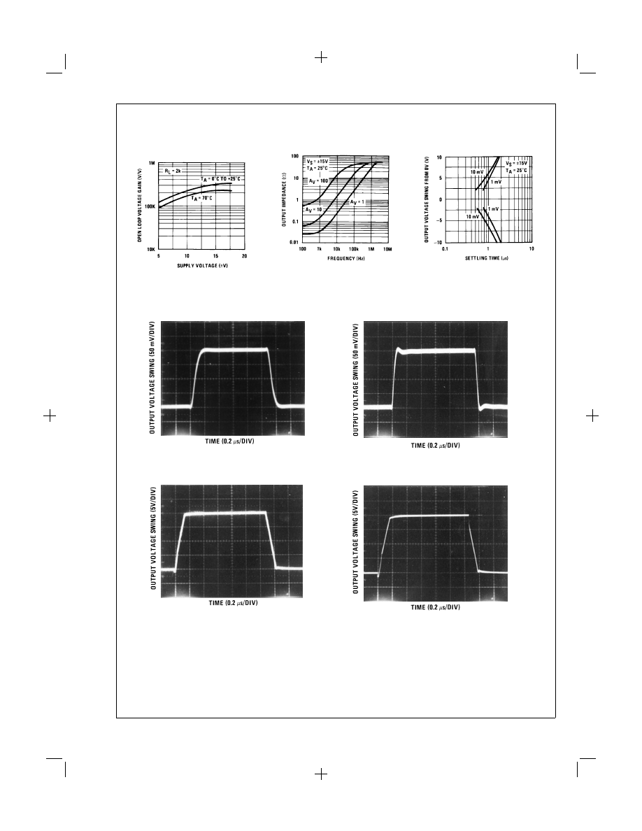
Typical Performance Characteristics
(Continued)
Pulse Response
Open Loop Voltage
Gain (V/V)
DS005648-32
Output Impedance
DS005648-33
Inverter Settling Time
DS005648-34
Small Signal Inverting
DS005648-4
Small Signal Non-Inverting
DS005648-5
Large Signal Inverting
DS005648-6
Large Signal Non-Inverting
DS005648-7
PrintDate=1998/04/07 PrintTime=13:52:35 38265 ds005648 Rev. No. 3
cmserv
Proof
6
www.national.com
6
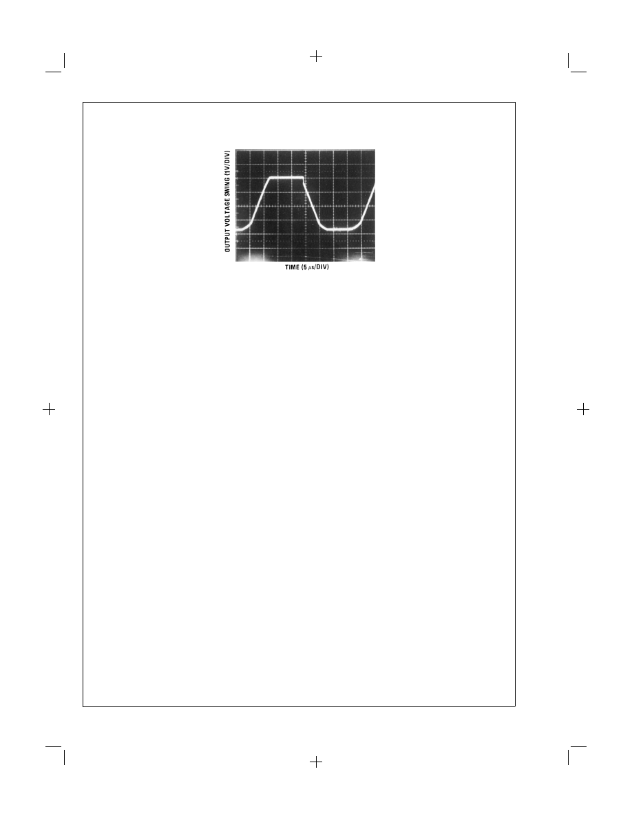
Pulse Response
(Continued)
Application Hints
The LF351 is an op amp with an internally trimmed input off-
set voltage and JFET input devices (BI-FET II
™
). These
JFETs have large reverse breakdown voltages from gate to
source and drain eliminating the need for clamps across the
inputs. Therefore, large differential input voltages can easily
be accommodated without a large increase in input current.
The maximum differential input voltage is independent of the
supply voltages. However, neither of the input voltages
should be allowed to exceed the negative supply as this will
cause large currents to flow which can result in a destroyed
unit.
Exceeding the negative common-mode limit on either input
will force the output to a high state, potentially causing a re-
versal of phase to the output.
Exceeding the negative common-mode limit on both inputs
will force the amplifier output to a high state. In neither case
does a latch occur since raising the input back within the
common-mode range again puts the input stage and thus
the amplifier in a normal operating mode.
Exceeding the positive common-mode limit on a single input
will not change the phase of the output; however, if both in-
puts exceed the limit, the output of the amplifier will be forced
to a high state.
The amplifier will operate with a common-mode input voltage
equal to the positive supply; however, the gain bandwidth
and slew rate may be decreased in this condition. When the
negative common-mode voltage swings to within 3V of the
negative supply, an increase in input offset voltage may oc-
cur.
The LF351 is biased by a zener reference which allows nor-
mal circuit operation on
±
4V power supplies. Supply volt-
ages less than these may result in lower gain bandwidth and
slew rate.
The LF351 will drive a 2 k
Ω¦
load resistance to
±
10V over the
full temperature range of 0°C to +70°C. If the amplifier is
forced to drive heavier load currents, however, an increase
in input offset voltage may occur on the negative voltage
swing and finally reach an active current limit on both posi-
tive and negative swings.
Precautions should be taken to ensure that the power supply
for the integrated circuit never becomes reversed in polarity
or that the unit is not inadvertently installed backwards in a
socket as an unlimited current surge through the resulting
forward diode within the IC could cause fusing of the internal
conductors and result in a destroyed unit.
As with most amplifiers, care should be taken with lead
dress, component placement and supply decoupling in order
to ensure stability. For example, resistors from the output to
an input should be placed with the body close to the input to
minimize pick-up and maximize the frequency of the feed-
back pole by minimizing the capacitance from the input to
ground.
A feedback pole is created when the feedback around any
amplifier is resistive. The parallel resistance and capacitance
from the input of the device (usually the inverting input) to AC
ground set the frequency of the pole. In many instances the
frequency of this pole is much greater than the expected 3
dB frequency of the closed loop gain and consequently there
is negligible effect on stability margin. However, if the feed-
back pole is less than approximately 6 times the expected 3
dB frequency a lead capacitor should be placed from the out-
put to the input of the op amp. The value of the added ca-
pacitor should be such that the RC time constant of this ca-
pacitor and the resistance it parallels is greater than or equal
to the original feedback pole time constant.
Current Limit (R
L
=100
Ω¦
)
DS005648-8
7
www.national.com
PrintDate=1998/04/07 PrintTime=13:52:35 38265 ds005648 Rev. No. 3
cmserv
Proof
7
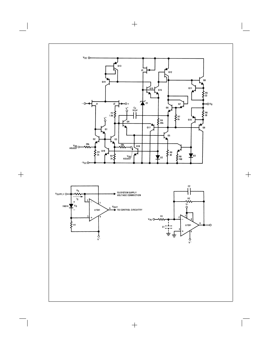
Detailed Schematic
Typical Applications
DS005648-9
Supply Current Indicator/Limiter
DS005648-40
V
OUT
switches high when R
S
I
S
>
V
D
Hi-Z
IN
Inverting Amplifier
DS005648-41
Parasitic input capacitance C1
(3 pF for LF351 plus any additional layout
capacitance) interacts with feedback elements and creates undesirable
high frequency pole. To compensate, add C2 such that: R2C2
R1C1.
PrintDate=1998/04/07 PrintTime=13:52:35 38265 ds005648 Rev. No. 3
cmserv
Proof
8
www.national.com
8
Typical Applications
(Continued)
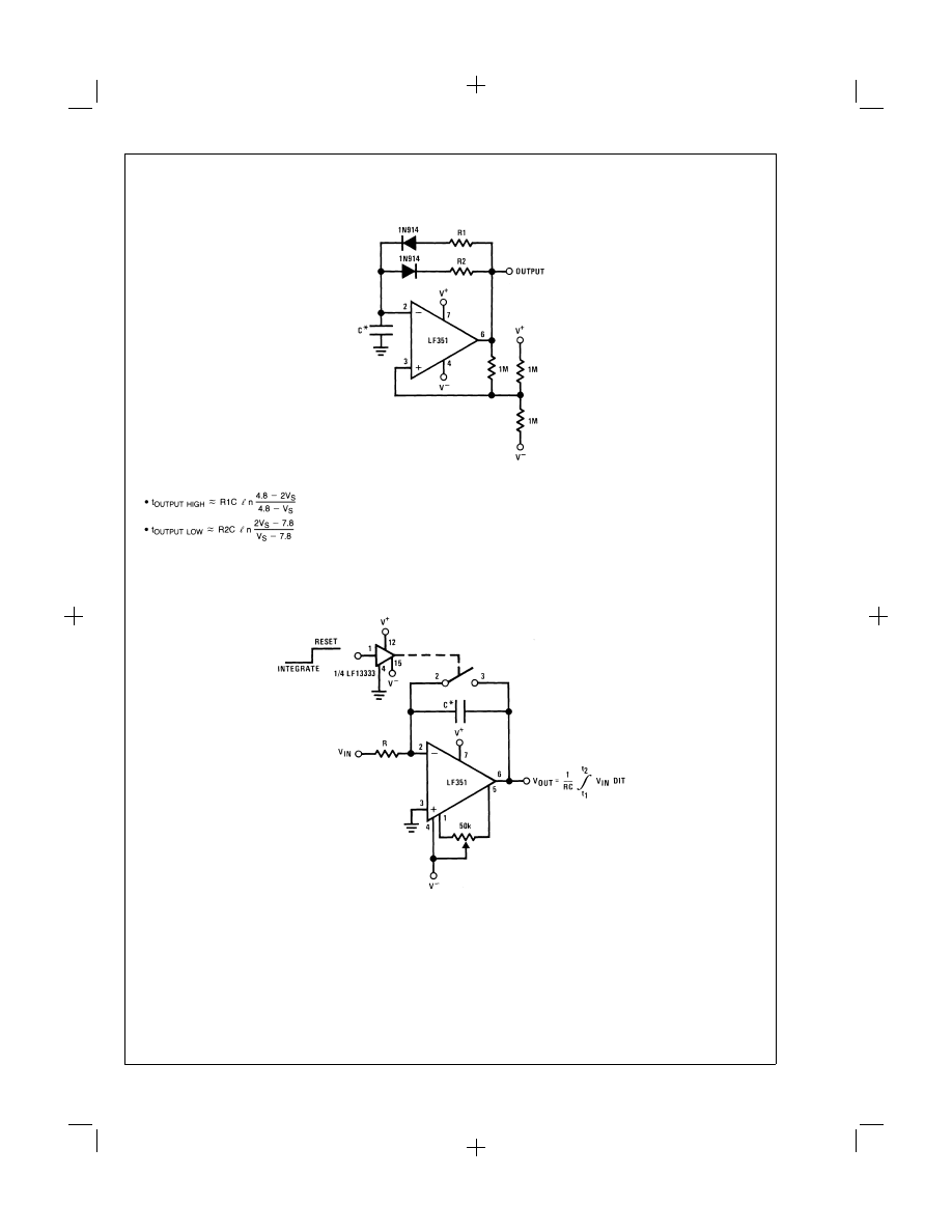
Ultra-Low (or High) Duty Cycle Pulse Generator
DS005648-42
where V
S
= V
+
+ |V
-
|
*low leakage capacitor
Long Time Integrator
DS005648-43
*Low leakage capacitor
50k pot used for less sensitive V
OS
adjust
9
www.national.com
PrintDate=1998/04/07 PrintTime=13:52:35 38265 ds005648 Rev. No. 3
cmserv
Proof
9
Book
Extract
End

THIS PAGE IS IGNORED IN THE DATABOOK
PrintDate=1998/04/07 PrintTime=13:52:35 38265 ds005648 Rev. No. 3
cmserv
Proof
10
10
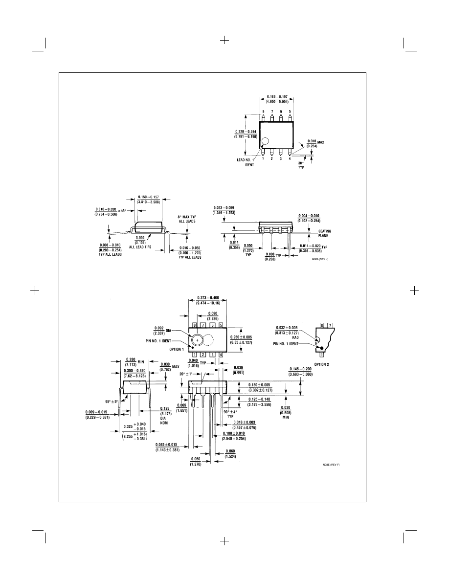
Physical Dimensions
inches (millimeters) unless otherwise noted
SO Package (M)
Order Number LF351M
NS Package Number M08A
Molded Dual-In-Line Package (N)
Order Number LF351N
NS Package Number N08E
11
www.national.com
11
PrintDate=1998/04/07 PrintTime=13:52:35 38265 ds005648 Rev. No. 3
cmserv
Proof
11
LIFE SUPPORT POLICY
NATIONALS PRODUCTS ARE NOT AUTHORIZED FOR USE AS CRITICAL COMPONENTS IN LIFE SUPPORT DE-
VICES OR SYSTEMS WITHOUT THE EXPRESS WRITTEN APPROVAL OF THE PRESIDENT OF NATIONAL SEMI-
CONDUCTOR CORPORATION. As used herein:
1. Life support devices or systems are devices or sys-
tems which, (a) are intended for surgical implant into
the body, or (b) support or sustain life, and whose fail-
ure to perform when properly used in accordance
with instructions for use provided in the labeling, can
be reasonably expected to result in a significant injury
to the user.
2. A critical component in any component of a life support
device or system whose failure to perform can be rea-
sonably expected to cause the failure of the life support
device or system, or to affect its safety or effectiveness.
National Semiconductor
Corporation
Americas
Tel: 1-800-272-9959
Fax: 1-800-737-7018
Email: support@nsc.com
www.national.com
National Semiconductor
Europe
Fax: +49 (0) 1 80-530 85 86
Email: europe.support@nsc.com
Deutsch Tel: +49 (0) 1 80-530 85 85
English
Tel: +49 (0) 1 80-532 78 32
Français Tel: +49 (0) 1 80-532 93 58
Italiano
Tel: +49 (0) 1 80-534 16 80
National Semiconductor
Asia Pacific Customer
Response Group
Tel: 65-2544466
Fax: 65-2504466
Email: sea.support@nsc.com
National Semiconductor
Japan Ltd.
Tel: 81-3-5620-6175
Fax: 81-3-5620-6179
LF351
W
ide
Bandwidth
JFET
Input
Operational
Amplifier
PrintDate=1998/04/07 PrintTime=13:52:35 38265 ds005648 Rev. No. 3
cmserv
Proof
12
National does not assume any responsibility for use of any circuitry described, no circuit patent licenses are implied and National reserves the right at any time without notice to change said circuitry and specifications.

IMPORTANT NOTICE
Texas Instruments Incorporated and its subsidiaries (TI) reserve the right to make corrections, modifications, enhancements, improvements,
and other changes to its products and services at any time and to discontinue any product or service without notice. Customers should
obtain the latest relevant information before placing orders and should verify that such information is current and complete. All products are
sold subject to TI
s terms and conditions of sale supplied at the time of order acknowledgment.
TI warrants performance of its hardware products to the specifications applicable at the time of sale in accordance with TI
s standard
warranty. Testing and other quality control techniques are used to the extent TI deems necessary to support this warranty. Except where
mandated by government requirements, testing of all parameters of each product is not necessarily performed.
TI assumes no liability for applications assistance or customer product design. Customers are responsible for their products and
applications using TI components. To minimize the risks associated with customer products and applications, customers should provide
adequate design and operating safeguards.
TI does not warrant or represent that any license, either express or implied, is granted under any TI patent right, copyright, mask work right,
or other TI intellectual property right relating to any combination, machine, or process in which TI products or services are used. Information
published by TI regarding third-party products or services does not constitute a license from TI to use such products or services or a
warranty or endorsement thereof. Use of such information may require a license from a third party under the patents or other intellectual
property of the third party, or a license from TI under the patents or other intellectual property of TI.
Reproduction of TI information in TI data books or data sheets is permissible only if reproduction is without alteration and is accompanied
by all associated warranties, conditions, limitations, and notices. Reproduction of this information with alteration is an unfair and deceptive
business practice. TI is not responsible or liable for such altered documentation. Information of third parties may be subject to additional
restrictions.
Resale of TI products or services with statements different from or beyond the parameters stated by TI for that product or service voids all
express and any implied warranties for the associated TI product or service and is an unfair and deceptive business practice. TI is not
responsible or liable for any such statements.
TI products are not authorized for use in safety-critical applications (such as life support) where a failure of the TI product would reasonably
be expected to cause severe personal injury or death, unless officers of the parties have executed an agreement specifically governing
such use. Buyers represent that they have all necessary expertise in the safety and regulatory ramifications of their applications, and
acknowledge and agree that they are solely responsible for all legal, regulatory and safety-related requirements concerning their products
and any use of TI products in such safety-critical applications, notwithstanding any applications-related information or support that may be
provided by TI. Further, Buyers must fully indemnify TI and its representatives against any damages arising out of the use of TI products in
such safety-critical applications.
TI products are neither designed nor intended for use in military/aerospace applications or environments unless the TI products are
specifically designated by TI as military-grade or
"
enhanced plastic.
"
Only products designated by TI as military-grade meet military
specifications. Buyers acknowledge and agree that any such use of TI products which TI has not designated as military-grade is solely at
the Buyer
'
s risk, and that they are solely responsible for compliance with all legal and regulatory requirements in connection with such use.
TI products are neither designed nor intended for use in automotive applications or environments unless the specific TI products are
designated by TI as compliant with ISO/TS 16949 requirements. Buyers acknowledge and agree that, if they use any non-designated
products in automotive applications, TI will not be responsible for any failure to meet such requirements.
Following are URLs where you can obtain information on other Texas Instruments products and application solutions:
Products
Applications
Audio
Communications and Telecom
Amplifiers
Computers and Peripherals
Data Converters
Consumer Electronics
DLP
®
Products
Energy and Lighting
DSP
Industrial
Clocks and Timers
Medical
Interface
Security
Logic
Space, Avionics and Defense
Power Mgmt
Transportation and Automotive
Microcontrollers
Video and Imaging
RFID
OMAP Mobile Processors
Wireless Connectivity
TI E2E Community Home Page
Mailing Address: Texas Instruments, Post Office Box 655303, Dallas, Texas 75265
Copyright
©
2011, Texas Instruments Incorporated

