| Secciones |
|---|
| Foros Electrónica |
|
|
| Boletines de correo |
 |

LF155, , , LF257
LF355, , LF357
SNOSBH0D - MAY 2000 - REVISED NOVEMBER 2015
LFx5x JFET Input Operational Amplifiers
1 Features
2 Applications
1
Advantages
Precision High-Speed Integrators
Fast D/A and A/D Converters
-
Replace Expensive Hybrid and Module FET
Op Amps
High Impedance Buffers
-
Rugged JFETs Allow Blow-Out Free Handling
Wideband, Low Noise, Low Drift Amplifiers
Compared With MOSFET Input Devices
Logarithmic Amplifiers
-
Excellent for Low Noise Applications Using
Photocell Amplifiers
Either High or Low Source ImpedanceVery
Sample and Hold Circuits
Low 1/f Corner
-
Offset Adjust Does Not Degrade Drift or
3 Description
Common-Mode Rejection as in Most
The LFx5x devices are the first monolithic JFET input
Monolithic Amplifiers
operational amplifiers to incorporate well-matched,
-
New Output Stage Allows Use of Large
high-voltage JFETs on the same chip with standard
bipolar transistors (BI-FET™ Technology). These
Capacitive Loads (5,000 pF) Without Stability
amplifiers
feature
low
input
bias
and
offset
Problems
currents/low offset voltage and offset voltage drift,
-
Internal Compensation and Large Differential
coupled with offset adjust, which does not degrade
Input Voltage Capability
drift or common-mode rejection. The devices are also
Common Features
designed
for
high
slew
rate,
wide
bandwidth,
extremely fast settling time, low voltage and current
-
Low Input Bias Current: 30 pA
noise and a low 1/f noise corner.
-
Low Input Offset Current: 3 pA
-
High Input Impedance: 10
12
Ω
Device
-
Low Input Noise Current: 0.01 pA/
√Hz
PART NUMBER
PACKAGE
BODY SIZE (NOM)
-
High Common-Mode Rejection Ratio: 100 dB
SOIC (8)
4.90 mm × 3.91 mm
LFx5x
TO-CAN (8)
9.08 mm × 9.08 mm
-
Large DC Voltage Gain: 106 dB
PDIP (8)
9.81 mm × 6.35 mm
Uncommon Features
(1) For all available packages, see the orderable addendum at
-
Extremely Fast Settling Time to 0.01%:
the end of the data sheet.
-
4
μs for the LFx55 devices
-
1.5
μs for the LFx56
Simplified Schematic
-
1.5
μs for the LFx57 (A
V
= 5)
-
Fast Slew Rate:
-
5 V/ µs for the LFx55
-
12 V/ µs for the LFx56
-
50 V/ µs for the LFx57 (A
V
= 5)
-
Wide Gain Bandwidth:
-
2.5 MHz for the LFx55 devices
-
5 MHz for the LFx56
-
20 MHz for the LFx57 (A
V
= 5)
-
Low Input Noise Voltage:
-
20 nV/
√Hz for the LFx55
3 pF in LF357 series
-
12 nV/
√Hz for the LFx56
-
12 nV/
√Hz for the LFx57 (A
V
= 5)
1
An IMPORTANT NOTICE at the end of this data sheet addresses availability, warranty, changes, use in safety-critical applications,
intellectual property matters and other important disclaimers. PRODUCTION DATA.

LF155, , LF257
LF355, LF357
SNOSBH0D - MAY 2000 - REVISED NOVEMBER 2015
Table of Contents
7.2
Functional Block Diagram .......................................
1
Features ..................................................................
7.3
Feature Description.................................................
2
Applications ...........................................................
7.4
Device Functional Modes........................................
3
Description .............................................................
8
Application and Implementation ........................
4
Revision History.....................................................
8.1
Application Information............................................
5
Pin Configuration and Functions .........................
8.2
Typical Application ..................................................
6
Specifications.........................................................
8.3
System Examples ...................................................
6.1
Absolute Maximum Ratings ......................................
9
Power Supply Recommendations ......................
6.2
ESD Ratings..............................................................
10
Layout...................................................................
6.3
Recommended Operating Conditions .......................
10.1
Layout Guidelines .................................................
6.4
Thermal Information ..................................................
10.2
Layout Example ....................................................
6.5
AC Electrical Characteristics, T
A
= T
J
= 25 °C, V
S
=
±15 V..........................................................................
11
Device and Documentation Support .................
6.6
DC Electrical Characteristics, T
A
= T
J
= 25 °C, V
S
=
11.1
Related Links ........................................................
±15 V..........................................................................
11.2
Community Resources..........................................
6.7
DC Electrical Characteristics ....................................
11.3
Trademarks ...........................................................
6.8
Power Dissipation Ratings ........................................
11.4
Electrostatic Discharge Caution ............................
6.9
Typical Characteristics ..............................................
11.5
Glossary ................................................................
7
Detailed Description ............................................
12
Mechanical, Packaging, and Orderable
7.1
Overview .................................................................
Information ...........................................................
4 Revision History
NOTE: Page numbers for previous revisions may differ from page numbers in the current version.
Changes from Revision C (March 2013) to Revision D
Page
Added Pin Configuration and Functions section, ESD Ratings table, Thermal Information table, Feature Description
section, Device Functional Modes, Application and Implementation section, Power Supply Recommendations
section, Layout section, Device and Documentation Support section, and Mechanical, Packaging, and Orderable
Information section ................................................................................................................................................................
Removed T
HIGH
parameter as it is redundant to T
A
maximum ...............................................................................................
Changes from Revision B (March 2013) to Revision C
Page
Changed layout of National Data Sheet to TI format ...........................................................................................................
2
Copyright © 2000-2015, Texas Instruments Incorporated
LF155, , , LF257
LF355, , LF357
SNOSBH0D - MAY 2000 - REVISED NOVEMBER 2015
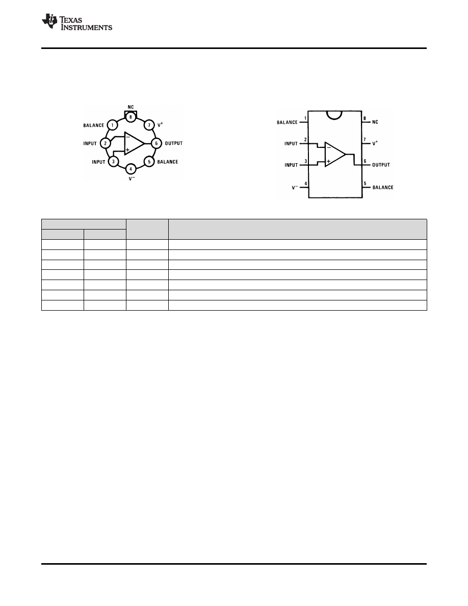
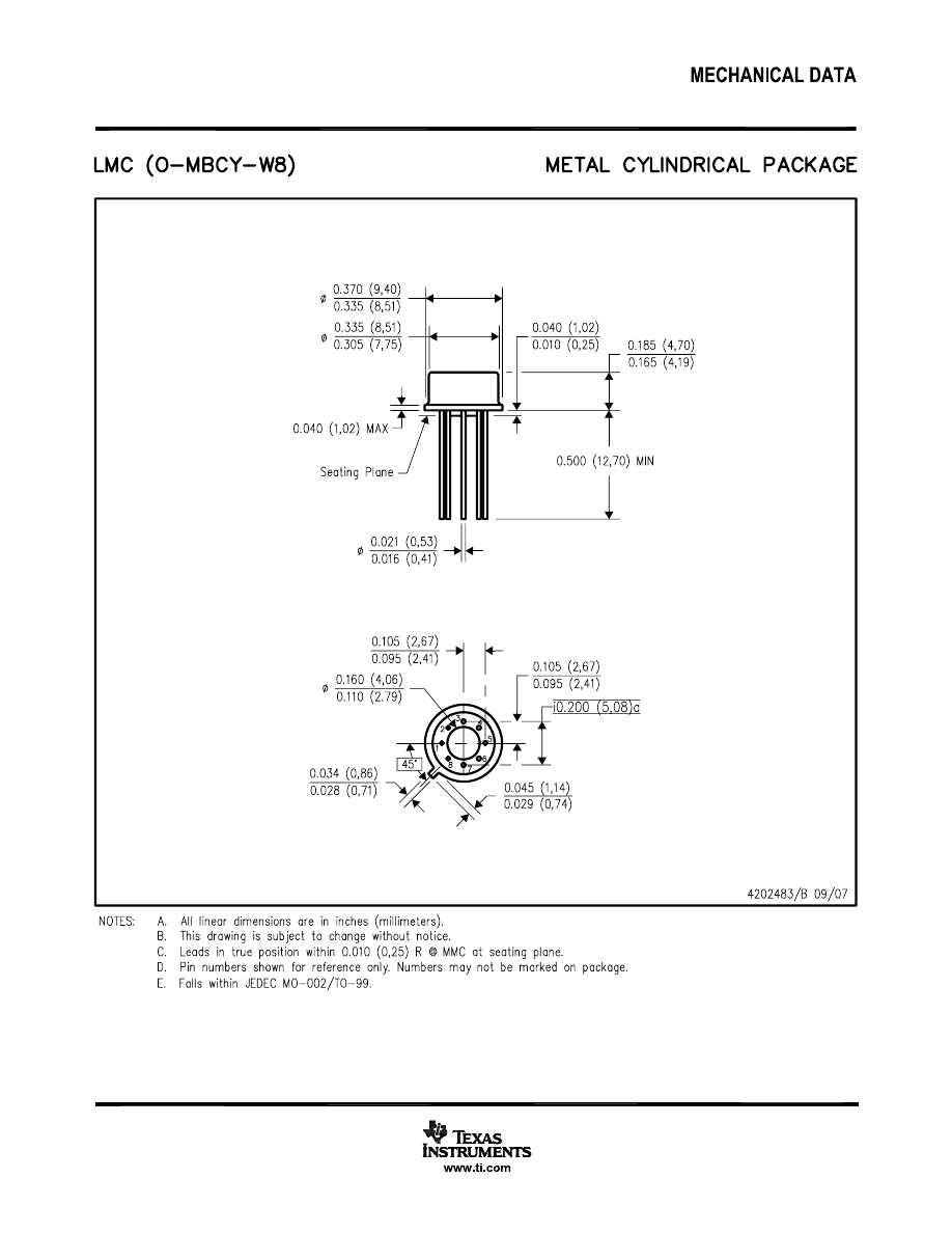
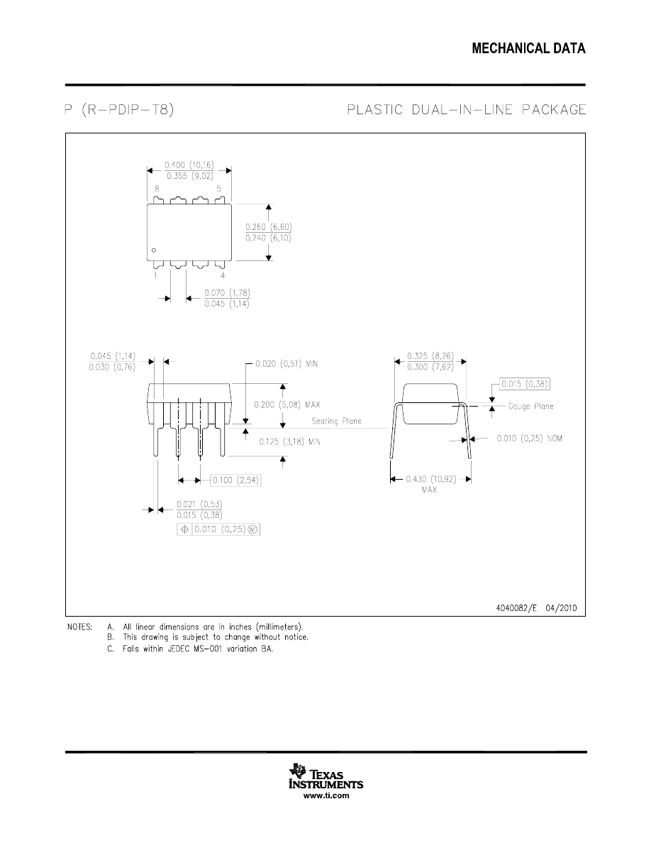
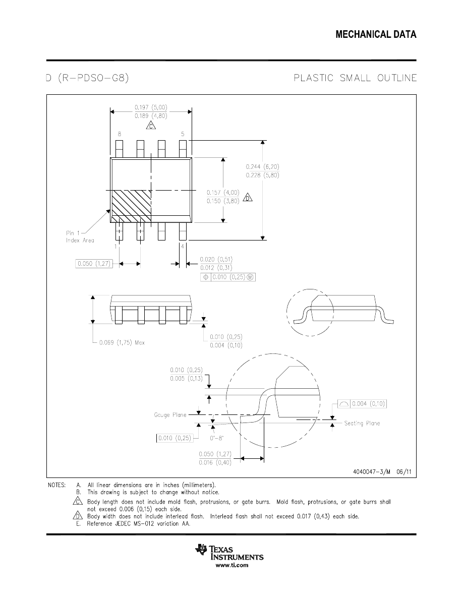
5 Pin Configuration and Functions
LMC Package
D or P Package
8-Pin TO-99
8-Pin SOIC or PDIP
Top View
Top View
Available per JM38510/11401 or
JM38510/11402
Pin Functions
PIN
I/O
DESCRIPTION
NAME
NO.
BALANCE
1, 5
I
Balance for input offset voltage
+INPUT
3
I
Noninverting input
-INPUT
2
I
Inverting input
NC
8
No connection
OUTPUT
6
O
Output
V+
7
Positive power supply
V-
4
Negative power supply
Copyright © 2000-2015, Texas Instruments Incorporated
3
LF155, , LF257
LF355, LF357
SNOSBH0D - MAY 2000 - REVISED NOVEMBER 2015
6 Specifications
6.1 Absolute Maximum Ratings
over operating free-air temperature range (unless otherwise noted)
(1) (2) (3)
MIN
MAX
UNIT
LF155x, LF256x, LF356B
±22
Supply voltage
V
LF35x
±18
LF15x, LF25x, LF356B
±40
Differential input voltage
V
LF35x
±30
LF15x, LF25x, LF356B
±20
Input voltage
(4)
V
LF35x
±16
Output short circuit duration
Continuous
LF15x
150
LMC package
LF25x, LF356B, LF35x
115
T
JMAX
°C
P package
LF25x, LF356B, LF35x
100
D package
LF25x, LF356B, LF35x
100
TO-99 package
Soldering (10 sec.)
300
Soldering
PDIP package
Soldering (10 sec.)
260
information
°C
(lead temp.)
Vapor phase (60 sec.)
LF25x, LF356B, LF35x
215
SOIC package
Infrared (15 sec.)
LF25x, LF356B, LF35x
220
Storage temperature, T
stg
-65
150
°C
(1)
Stresses beyond those listed under Absolute Maximum Ratings may cause permanent damage to the device. These are stress ratings
only, which do not imply functional operation of the device at these or any other conditions beyond those indicated under Recommended
Operating Conditions. Exposure to absolute-maximum-rated conditions for extended periods may affect device reliability.
(2)
The maximum power dissipation for these devices must be derated at elevated temperatures and is dictated by T
JMAX
,
Θ
JA
, and the
ambient temperature, T
A
. The maximum available power dissipation at any temperature is P
D
= (T
JMAX
- T
A
) /
Θ
JA
or the 25 °C P
dMAX
,
whichever is less.
(3)
If Military/Aerospace specified devices are required, contact the TI Sales Office/Distributors for availability and specifications.
(4)
Unless otherwise specified the absolute maximum negative input voltage is equal to the negative power supply voltage.
6.2 ESD Ratings
VALUE
UNIT
V
(ESD)
Electrostatic discharge
Human body model (HBM), per ANSI/ESDA/JEDEC JS-001
(1) (2)
±1000
V
(1)
JEDEC document JEP155 states that 500-V HBM allows safe manufacturing with a standard ESD control process.
(2)
100 pF discharged through 1.5-k
Ω resistor
6.3 Recommended Operating Conditions
over operating free-air temperature range (unless otherwise noted)
MIN
NOM
MAX
UNIT
LF15x
±15
V
S
±20
LF25x
±15
V
S
±20
Supply voltage, V
S
V
LF356B
±15
V
S
±20
LF35x
±15
LF15x
-55
T
A
125
LF25x
-25
T
A
85
T
A
°C
LF356B
0
T
A
70
LF35x
0
T
A
70
4
Copyright © 2000-2015, Texas Instruments Incorporated
LF155, , , LF257
LF355, , LF357
SNOSBH0D - MAY 2000 - REVISED NOVEMBER 2015
6.4 Thermal Information
LF155, LF156, LF355, LF357
LF356
D
THERMAL METRIC
(1)
P (PDIP)
LMC (TO-99)
P (PDIP)
UNIT
(SOIC)
8 PINS
8 PINS
8 PINS
8 PINS
Junction-to-ambient thermal resistance
130
195
55.2
R
ΘJA
Still Air
160
°C/W
400 LF/Min Air Flow
65
R
ΘJC(top)
Junction-to-case (top) thermal resistance
23
44.5
°C/W
R
ΘJB
Junction-to-board thermal resistance
32.4
°C/W
Ï
JT
Junction-to-top characterization parameter
21.7
°C/W
Ï
JB
Junction-to-board characterization parameter
32.3
°C/W
(1)
For more information about traditional and new thermal metrics, see the Semiconductor and IC Package Thermal Metrics application
report,
6.5 AC Electrical Characteristics, T
A
= T
J
= 25 °C, V
S
= ±15 V
PARAMETER
TEST CONDITIONS
MIN
TYP
MAX
UNIT
LFx55
5
LF15x: A
V
= 1
LFx56, LF356B
7.5
SR
Slew Rate
V/
μs
LFx56, LF356B
12
LF357: A
V
= 5
LFx57
50
LFx55
2.5
Gain Bandwidth
GBW
LFx56, LF356B
5
MHz
Product
LFx57
20
LFx55
4
Settling Time to
t
s
LFx56, LF356B
1.5
μs
0.01%
(1)
LFx57
1.5
LFx55
25
f = 100 Hz
LFx56, LF356B
15
nV/
√Hz
LFx57
15
Equivalent Input
e
n
R
S
= 100
Ω
Noise Voltage
LFx55
20
f = 1000 Hz
LFx56, LF356B
12
nV/
√Hz
LFx57
12
LFx55
f = 100 Hz
LFx56, LF356B
0.01
pA/
√Hz
LFx57
Equivalent Input
i
n
Current Noise
LFx55
f = 1000 Hz
LFx56, LF356B
0.01
pA/
√Hz
LFx57
LFx55
Input
C
IN
LFx56, LF356B
3
pF
Capacitance
LFx57
(1)
Settling time is defined here, for a unity gain inverter connection using 2-k
Ω resistors for the LF15x. It is the time required for the error
voltage (the voltage at the inverting input pin on the amplifier) to settle to within 0.01% of its final value from the time a 10-V step input is
applied to the inverter. For the LF357, A
V
=
-5, the feedback resistor from output to input is 2 kΩ and the output step is 10 V (See
Copyright © 2000-2015, Texas Instruments Incorporated
5
LF155, , LF257
LF355, LF357
SNOSBH0D - MAY 2000 - REVISED NOVEMBER 2015
6.6 DC Electrical Characteristics, T
A
= T
J
= 25 °C, V
S
= ±15 V
PARAMETER
TEST CONDITIONS
MIN
TYP
MAX
UNIT
LF155
2
4
LF355
2
4
Supply current
LFx56, LF356B
5
7
mA
LF356
5
10
LF357
5
10
6.7 DC Electrical Characteristics
See
(1)
PARAMETER
TEST CONDITIONS
MIN
TYP
MAX
UNIT
LF15x, LF25x, LF356B
3
5
T
A
= 25 °C
LF35x
3
10
V
OS
Input offset voltage
R
S
= 50
Ω
LF15x
7
mV
Over
LF25x, LF356B
6.5
temperature
LF35x
13
Average TC of input
ΔV
OS
/
ΔT
R
S
= 50
Ω
LF15x, LF25x, LF356B, LF35x
5
μV/ °C
offset voltage
Change in average TC
μV/ °C
ΔTC/ΔV
OS
R
S
= 50
Ω
(2)
LF15x, LF25x, LF356B, LF35x
0.5
with V
OS
adjust
per mV
LF15x, LF25x, LF356B
3
20
T
J
= 25 °C
(1) (3)
pA
LF35x
3
50
I
OS
Input offset current
LF15x
20
T
J
≤ T
HIGH
LF25x, LF356B
1
nA
LF35x
2
LF15x, LF25x, LF356B
30
100
T
J
= 25 °C
(1) (3)
pA
LF35x
30
200
I
B
Input bias current
LF15x
50
T
J
≤ T
HIGH
LF25x, LF356B
5
nA
LF35x
8
R
IN
Input resistance
T
J
= 25 °C
LF15x, LF25x, LF356B, LF35x
Ω
10
12
LF15x, LF25x, LF356B
50
200
T
A
= 25 °C
V
S
= ±15 V,
LF35x
25
200
A
VOL
Large signal voltage gain
V
O
= ±10 V,
V/mV
LF15x, LF25x, LF356B
25
Over
R
L
= 2 k
Ω
temperature
LF35x
15
V
S
= ±15 V, R
L
= 10 k
Ω
LF15x, LF25x, LF356B, LF35x
±12
±13
V
O
Output voltage swing
V
V
S
= ±15 V, R
L
= 2 k
Ω
LF15x, LF25x, LF356B, LF35x
±10
±12
(1)
Unless otherwise stated, these test conditions apply:
LF15x
LF25x
LF356B
LF35x
Supply Voltage, V
S
±15 V
≤ V
S
≤ ±20 V
±15 V
≤ V
S
≤ ±20 V
±15 V
≤ V
S
≤ ±20 V
V
S
= ±15 V
T
A
-55 °C ≤ T
A
≤ +125 °C
-25 °C ≤ T
A
≤ +85 °C
0 °C
≤ T
A
≤ +70 °C
0 °C
≤ T
A
≤ +70 °C
T
HIGH
+125 °C
+85 °C
+70 °C
+70 °C
and V
OS
, I
B
and I
OS
are measured at V
CM
= 0.
(2)
The Temperature Coefficient of the adjusted input offset voltage changes only a small amount (0.5
μV/ °C typically) for each mV of
adjustment from its original unadjusted value. Common-mode rejection and open-loop voltage gain are also unaffected by offset
adjustment.
(3)
The input bias currents are junction leakage currents which approximately double for every 10 °C increase in the junction temperature,
T
J
. Due to limited production test time, the input bias currents measured are correlated to junction temperature. In normal operation the
junction temperature rises above the ambient temperature as a result of internal power dissipation, Pd. T
J
= T
A
+
Θ
JA
Pd where
Θ
JA
is
the thermal resistance from junction to ambient. Use of a heat sink is recommended if input bias current is to be kept to a minimum.
6
Copyright © 2000-2015, Texas Instruments Incorporated
LF155, , , LF257
LF355, , LF357
SNOSBH0D - MAY 2000 - REVISED NOVEMBER 2015
DC Electrical Characteristics (continued)
See
PARAMETER
TEST CONDITIONS
MIN
TYP
MAX
UNIT
LF15x, LF25x, LF356B
11
15.1
V
CM, High
LF35x
10
15.1
Input common-mode
V
CM
V
S
= ±15 V
V
voltage range
LF15x, LF25x, LF356B
-12
-11
V
CM, Low
LF35x
-12
-10
LF15x, LF25x, LF356B
85
100
Common-mode rejection
CMRR
dB
ratio
LF35x
80
100
LF15x, LF25x, LF356B
85
100
Supply voltage rejection
PSRR
dB
ratio
(4)
LF35x
80
100
(4)
Supply Voltage Rejection is measured for both supply magnitudes increasing or decreasing simultaneously, in accordance with common
practice.
6.8 Power Dissipation Ratings
MIN
MAX
UNIT
LF15x
560
LMC Package (Still Air)
LF25x, LF356B, LF35x
400
LF15x
1200
Power Dissipation at
LMC Package
mW
T
A
= 25 °C
(1) (2)
(400 LF/Min Air Flow)
LF25x, LF356B, LF35x
1000
P Package
LF25x, LF356B, LF35x
670
D Package
LF25x, LF356B, LF35x
380
(1)
The maximum power dissipation for these devices must be derated at elevated temperatures and is dictated by T
JMAX
,
Θ
JA
, and the
ambient temperature, T
A
. The maximum available power dissipation at any temperature is P
D
= (T
JMAX
- T
A
) /
Θ
JA
or the 25 °C P
dMAX
,
whichever is less.
(2)
Maximum power dissipation is defined by the package characteristics. Operating the part near the maximum power dissipation may
cause the part to operate outside specified limits.
Copyright © 2000-2015, Texas Instruments Incorporated
7
LF155, , LF257
LF355, LF357
SNOSBH0D - MAY 2000 - REVISED NOVEMBER 2015
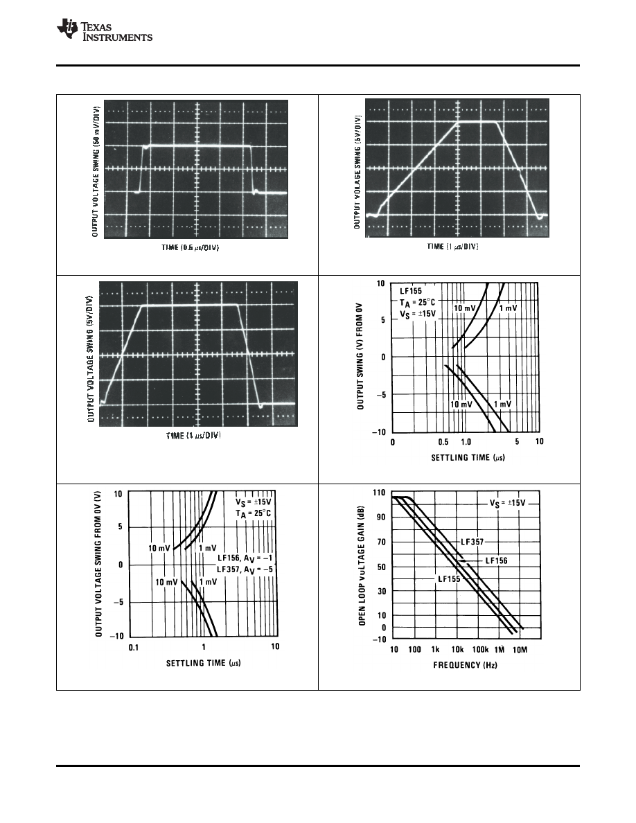
6.9 Typical Characteristics
6.9.1 Typical DC Performance Characteristics
Curves are for LF155 and LF156 unless otherwise specified.
Figure 2. Input Bias Current
Figure 1. Input Bias Current
Figure 4. Voltage Swing
Figure 3. Input Bias Current
Figure 5. Supply Current
Figure 6. Supply Current
8
Copyright © 2000-2015, Texas Instruments Incorporated
LF155, , , LF257
LF355, , LF357
SNOSBH0D - MAY 2000 - REVISED NOVEMBER 2015
Typical DC Performance Characteristics (continued)
Curves are for LF155 and LF156 unless otherwise specified.
Figure 8. Positive Current Limit
Figure 7. Negative Current Limit
Figure 10. Negative Common-Mode Input Voltage Limit
Figure 9. Positive Common-Mode Input Voltage Limit
Figure 12. Output Voltage Swing
Figure 11. Open-Loop Voltage Gain
Copyright © 2000-2015, Texas Instruments Incorporated
9
LF155, , LF257
LF355, LF357
SNOSBH0D - MAY 2000 - REVISED NOVEMBER 2015
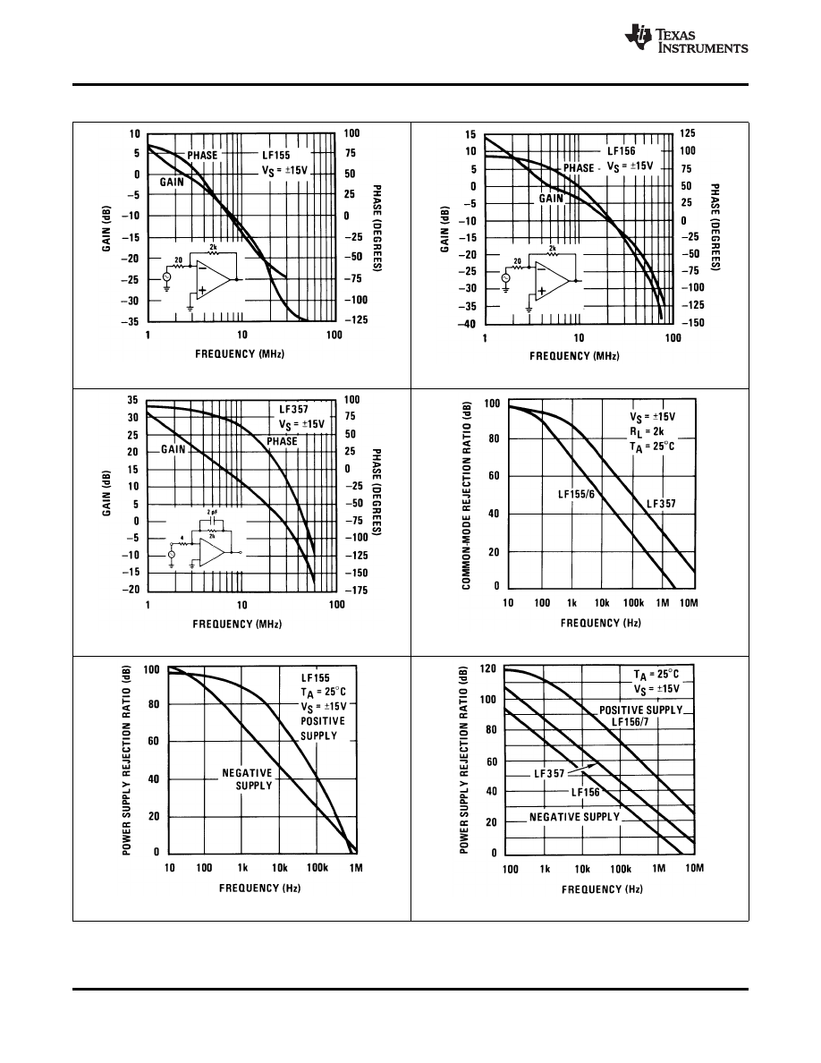
6.9.2 Typical AC Performance Characteristics
Figure 14. Gain Bandwidth
Figure 13. Gain Bandwidth
Figure 16. Output Impedance
Figure 15. Normalized Slew Rate
Figure 18. LF155 Small Signal Pulse Response, A
V
= +1
Figure 17. Output Impedance
10
Copyright © 2000-2015, Texas Instruments Incorporated
LF155, , , LF257
LF355, , LF357
SNOSBH0D - MAY 2000 - REVISED NOVEMBER 2015
Typical AC Performance Characteristics (continued)
Figure 20. LF155 Large Signal Pulse Response, A
V
= +1
Figure 19. LF156 Small Signal Pulse Response, A
V
= +1
Figure 21. LF156 Large Signal Puls Response, A
V
= +1
Figure 22. Inverter Settling Time
Figure 23. Inverter Settling Time
Figure 24. Open-Loop Frequency Response
Copyright © 2000-2015, Texas Instruments Incorporated
11
LF155, , LF257
LF355, LF357
SNOSBH0D - MAY 2000 - REVISED NOVEMBER 2015
Typical AC Performance Characteristics (continued)
Figure 25. Bode Plot
Figure 26. Bode Plot
Figure 27. Bode Plot
Figure 28. Common-Mode Rejection Ratio
Figure 29. Power Supply Rejection Ratio
Figure 30. Power Supply Rejection Ratio
12
Copyright © 2000-2015, Texas Instruments Incorporated
LF155, , , LF257
LF355, , LF357
SNOSBH0D - MAY 2000 - REVISED NOVEMBER 2015
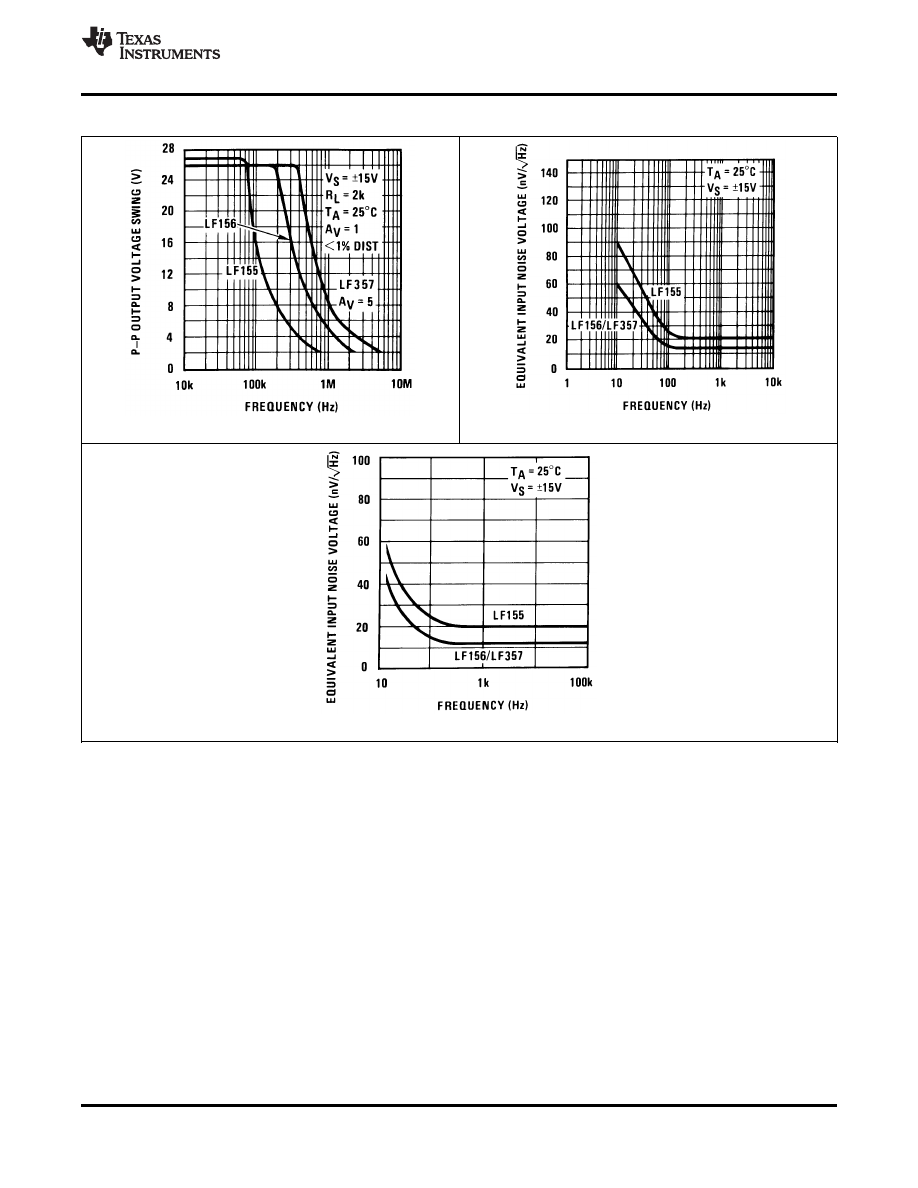
Typical AC Performance Characteristics (continued)
Figure 32. Equivalent Input Noise Voltage
Figure 31. Undistorted Output Voltage Swing
Figure 33. Equivalent Input Noise Voltage (Expanded Scale)
Copyright © 2000-2015, Texas Instruments Incorporated
13

LF155, , LF257
LF355, LF357
SNOSBH0D - MAY 2000 - REVISED NOVEMBER 2015
7 Detailed Description
7.1 Overview
These are the first monolithic JFET input operational amplifiers to incorporate well matched, high voltage JFETs
on the same chip with standard bipolar transistors (BI-FET Technology). These amplifiers feature low input bias
and offset currents, as well as low offset voltage and offset voltage drift, coupled with offset adjust which does
not degrade drift or common-mode rejection. These devices can replace expensive hybrid and module FET
operational amplifiers. Designed for low voltage and current noise and a low 1/f noise corner, these devices are
excellent for low noise applications using either high or low source impedance.
14
Copyright © 2000-2015, Texas Instruments Incorporated

LF155, , , LF257
LF355, , LF357
SNOSBH0D - MAY 2000 - REVISED NOVEMBER 2015
7.2 Functional Block Diagram
*C = 3 pF in LF357 series.
Figure 34. Detailed Schematic
Copyright © 2000-2015, Texas Instruments Incorporated
15

LF155, , LF257
LF355, LF357
SNOSBH0D - MAY 2000 - REVISED NOVEMBER 2015
7.3 Feature Description
7.3.1 Large Differential Input Voltage
These are operational amplifiers with JFET input devices. These JFETs have large reverse breakdown voltages
from gate to source and drain eliminating the need for clamps across the inputs. Therefore large differential input
voltages can easily be accommodated without a large increase in input current. The maximum differential input
voltage is independent of the supply voltages. However, neither of the input voltages should be allowed to
exceed the negative supply as this will cause large currents to flow which can result in a destroyed unit.
7.3.2 Large Common-Mode Input Voltage
These amplifiers will operate with the common-mode input voltage equal to the positive supply. In fact, the
common-mode voltage can exceed the positive supply by approximately 100 mV independent of supply voltage
and over the full operating temperature range. The positive supply can therefore be used as a reference on an
input as, for example, in a supply current monitor and/or limiter.
7.4 Device Functional Modes
The LFx5x has a single functional mode and operates according to the conditions listed in the
.
16
Copyright © 2000-2015, Texas Instruments Incorporated

LF155, , , LF257
LF355, , LF357
SNOSBH0D - MAY 2000 - REVISED NOVEMBER 2015
8 Application and Implementation
NOTE
Information in the following applications sections is not part of the TI component
specification, and TI does not warrant its accuracy or completeness. TIs customers are
responsible for determining suitability of components for their purposes. Customers should
validate and test their design implementation to confirm system functionality.
8.1 Application Information
These are op amps with JFET input devices. These JFETs have large reverse breakdown voltages from gate to
source and drain eliminating the need for clamps across the inputs. Therefore large differential input voltages can
easily be accommodated without a large increase in input current. The maximum differential input voltage is
independent of the supply voltages. However, neither of the input voltages should be allowed to exceed the
negative supply as this will cause large currents to flow which can result in a destroyed unit.
Exceeding the negative common-mode limit on either input will force the output to a high state, potentially
causing a reversal of phase to the output. Exceeding the negative common-mode limit on both inputs will force
the amplifier output to a high state. In neither case does a latch occur since raising the input back within the
common-mode range again puts the input stage and thus the amplifier in a normal operating mode.
Exceeding the positive common-mode limit on a single input will not change the phase of the output however, if
both inputs exceed the limit, the output of the amplifier will be forced to a high state.
These amplifiers will operate with the common-mode input voltage equal to the positive supply. In fact, the
common-mode voltage can exceed the positive supply by approximately 100 mV independent of supply voltage
and over the full operating temperature range. The positive supply can therefore be used as a reference on an
input as, for example, in a supply current monitor and/or limiter.
Precautions should be taken to ensure that the power supply for the integrated circuit never becomes reversed in
polarity or that the unit is not inadvertently installed backwards in a socket as an unlimited current surge through
the resulting forward diode within the IC could cause fusing of the internal conductors and result in a destroyed
unit.
All of the bias currents in these amplifiers are set by FET current sources. The drain currents for the amplifiers
are therefore essentially independent of supply voltage.
As with most amplifiers, care should be taken with lead dress, component placement and supply decoupling in
order to ensure stability. For example, resistors from the output to an input should be placed with the body close
to the input to minimize pick-up and maximize the frequency of the feedback pole by minimizing the capacitance
from the input to ground.
A feedback pole is created when the feedback around any amplifier is resistive. The parallel resistance and
capacitance from the input of the device (usually the inverting input) to AC ground set the frequency of the pole.
In many instances the frequency of this pole is much greater than the expected 3-dB frequency of the closed
loop gain and consequently there is negligible effect on stability margin. However, if the feedback pole is less
than approximately six times the expected 3-dB frequency a lead capacitor should be placed from the output to
the input of the op amp. The value of the added capacitor should be such that the RC time constant of this
capacitor and the resistance it parallels is greater than or equal to the original feedback pole time constant.
Copyright © 2000-2015, Texas Instruments Incorporated
17
LF155, , LF257
LF355, LF357
SNOSBH0D - MAY 2000 - REVISED NOVEMBER 2015
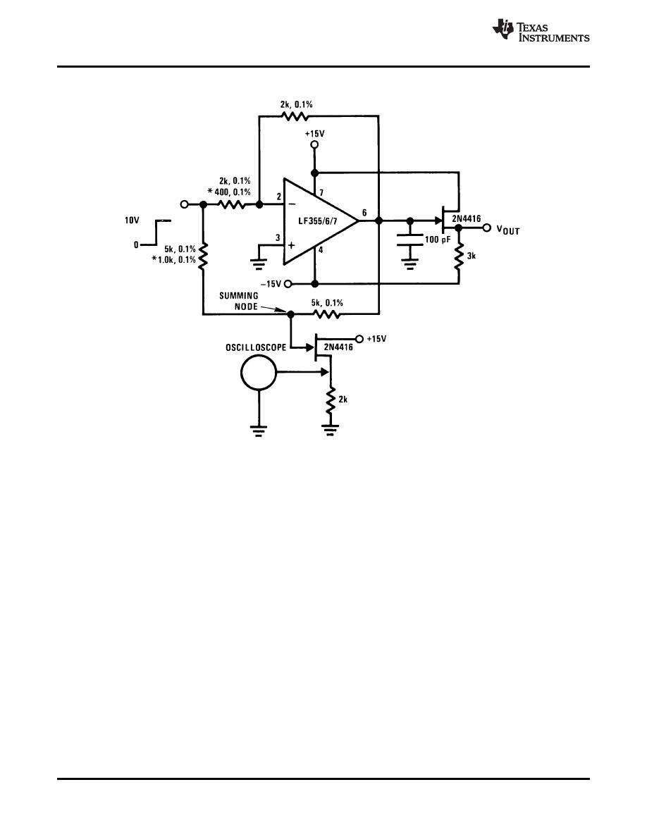
8.2 Typical Application
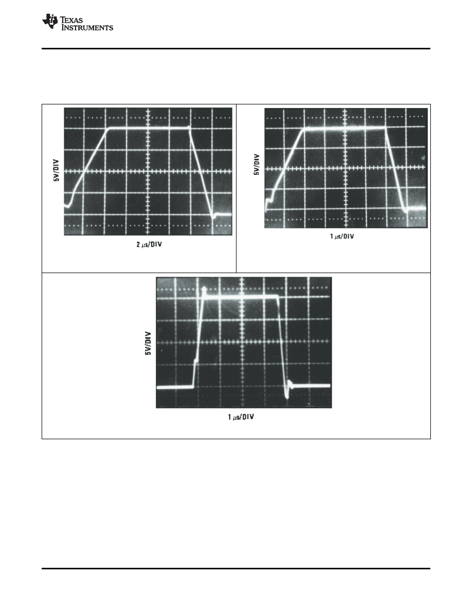
Figure 35. Settling Time Test Circuit
8.2.1 Design Requirements
Settling time is tested with the LF35x connected as unity gain inverter and LF357 connected for A
V
=
-5
8.2.2 Detailed Design Procedure
Connect the circuit components as shown in
In particular, use FET to isolate the probe capacitance.
Apply a 10-V step function to the input.
Use an oscilloscope to probe the circuit as shown in
.
18
Copyright © 2000-2015, Texas Instruments Incorporated
LF155, , , LF257
LF355, , LF357
SNOSBH0D - MAY 2000 - REVISED NOVEMBER 2015
Typical Application (continued)
8.2.3 Application Curves
Large Signal Inverter Output, V
OUT
(from Settling Time Circuit)
Figure 36. LF355
Figure 37. LF356
Figure 38. LF357
Copyright © 2000-2015, Texas Instruments Incorporated
19
LF155, , LF257
LF355, LF357
SNOSBH0D - MAY 2000 - REVISED NOVEMBER 2015
8.3 System Examples
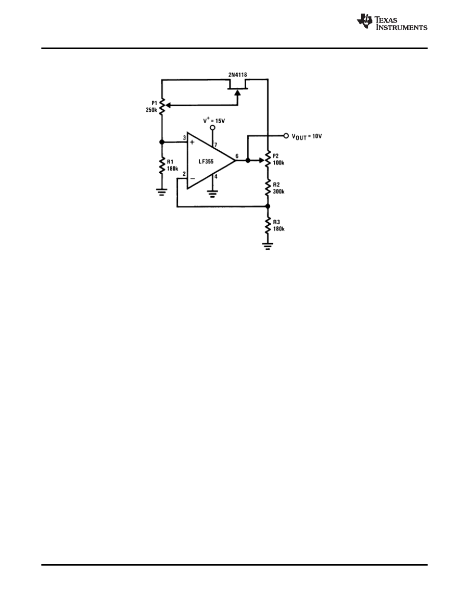
Figure 39. Low Drift Adjustable Voltage Reference
ΔV
OUT
/
ΔT = ±0.002%/ °C
All resistors and potentiometers should be wire-wound
P1: drift adjust
P2: V
OUT
adjust
Use LF155 for
-
Low I
B
-
Low drift
-
Low supply current
20
Copyright © 2000-2015, Texas Instruments Incorporated
LF155, , , LF257
LF355, , LF357
SNOSBH0D - MAY 2000 - REVISED NOVEMBER 2015
System Examples (continued)
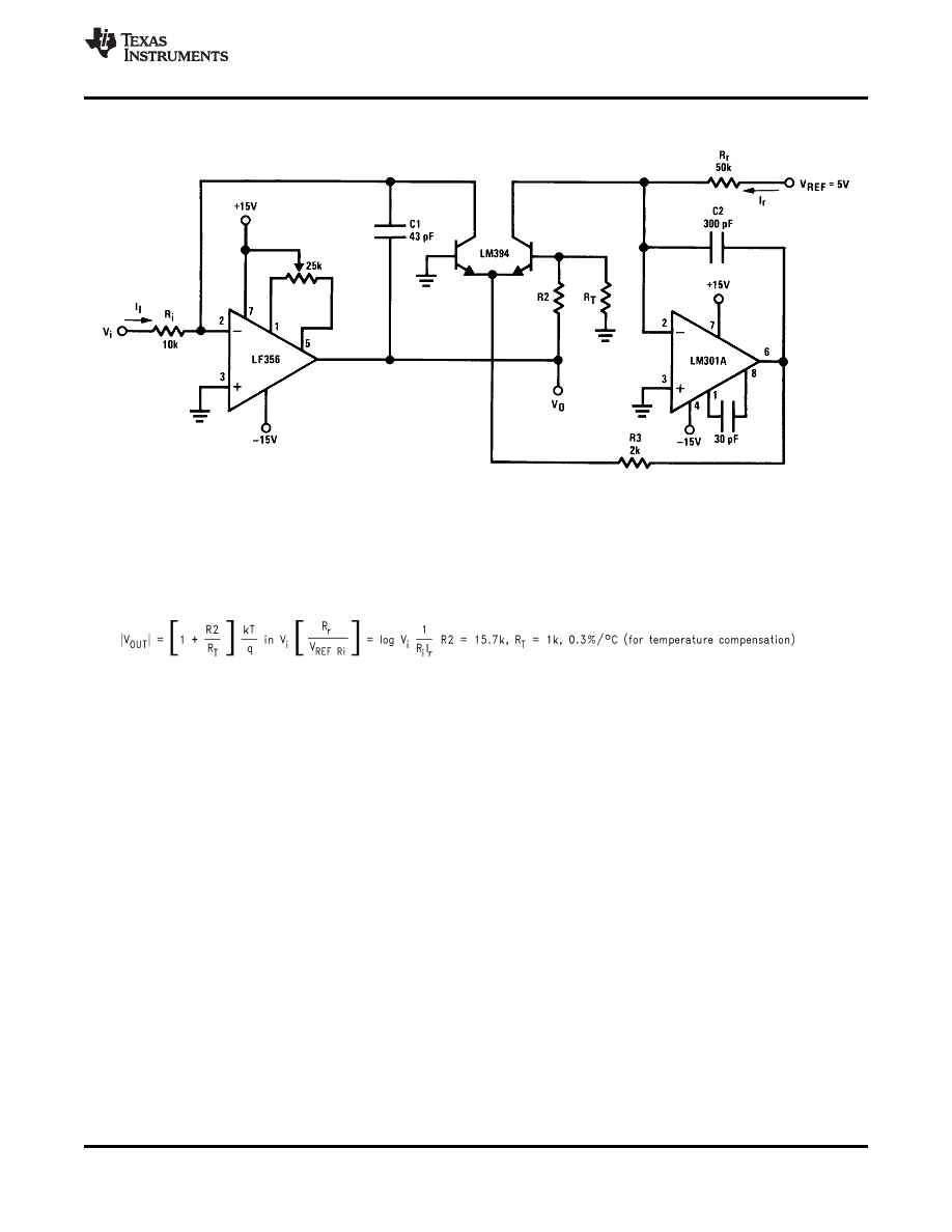
Figure 40. Fast Logarithmic Converter
Dynamic range: 100
μA ≤ I
i
≤ 1 mA (5 decades), |V
O
| = 1 V/decade
Transient response: 3
μs for ΔI
i
= 1 decade
C1, C2, R2, R3: added dynamic compensation
V
OS
adjust the LF156 to minimize quiescent error
R
T
: Tel Labs type Q81 + 0.3%/ °C
(1)
Copyright © 2000-2015, Texas Instruments Incorporated
21

LF155, , LF257
LF355, LF357
SNOSBH0D - MAY 2000 - REVISED NOVEMBER 2015
System Examples (continued)
Figure 41. Precision Current Monitor
V
O
= 5 R1/R2 (V/mA of I
S
)
R1, R2, R3: 0.1% resistors
Use LF155 for
-
Common-mode range to supply range
-
Low I
B
-
Low V
OS
-
Low Supply Current
22
Copyright © 2000-2015, Texas Instruments Incorporated
LF155, , , LF257
LF355, , LF357
SNOSBH0D - MAY 2000 - REVISED NOVEMBER 2015
System Examples (continued)
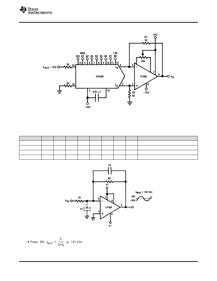
Figure 42. 8-Bit D/A Converter With Symmetrical Offset Binary Operation
R1, R2 should be matched within ±0.05%
Full-scale response time: 3
μs
Table 1. Bit Illustration of the 8-Bit D/A Converter
E
O
B1
B2
B3
B4
B5
B6
B7
B8
COMMENTS
+9.920
1
1
1
1
1
1
1
1
Positive Full-Scale
+0.040
1
0
0
0
0
0
0
0
(+) Zero-Scale
-0.040
0
1
1
1
1
1
1
1
(
-) Zero-Scale
-9.920
0
0
0
0
0
0
0
0
Negative Full-Scale
Figure 43. Wide BW Low Noise, Low Drift Amplifier
(2)
Copyright © 2000-2015, Texas Instruments Incorporated
23
LF155, , LF257
LF355, LF357
SNOSBH0D - MAY 2000 - REVISED NOVEMBER 2015
Parasitic input capacitance C1
(3 pF for LF155, LF156 and LF357 plus any additional layout capacitance)
interacts with feedback elements and creates undesirable high frequency pole. To compensate add C2 such that:
R2 C2
R1 C1.
Figure 44. Boosting the LF156 With a Current Amplifier
I
OUT(MAX)
150 mA (will drive R
L
≥ 100 Ω)
(3)
No additional phase shift added by the current amplifier
Figure 45. Decades VCO
24
Copyright © 2000-2015, Texas Instruments Incorporated
LF155, , , LF257
LF355, , LF357
SNOSBH0D - MAY 2000 - REVISED NOVEMBER 2015
R1, R4 matched. Linearity 0.1% over 2 decades.
(4)
Figure 46. Isolating Large Capacitive Loads
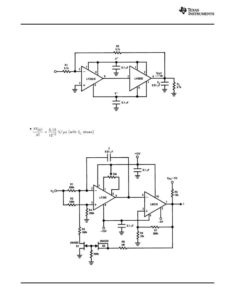
Overshoot 6%
t
s
10
μs
When driving large C
L
, the V
OUT
slew rate determined by C
L
and I
OUT(MAX)
:
(5)
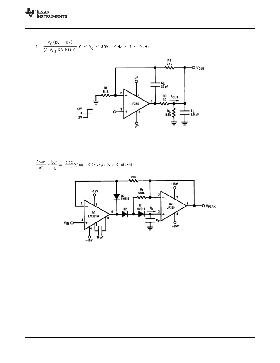
Figure 47. Low Drift Peak Detector
By adding D1 and R
f
, V
D1
= 0 during hold mode. Leakage of D2 provided by feedback path through R
f
.
Leakage of circuit is essentially I
b
(LF155, LF156) plus capacitor leakage of Cp.
Diode D3 clamps V
OUT
(A1) to V
IN
- V
D3
to improve speed and to limit reverse bias of D2.
Maximum input frequency should be << ½
ÏR
f
C
D2
where C
D2
is the shunt capacitance of D2.
Copyright © 2000-2015, Texas Instruments Incorporated
25
LF155, , LF257
LF355, LF357
SNOSBH0D - MAY 2000 - REVISED NOVEMBER 2015
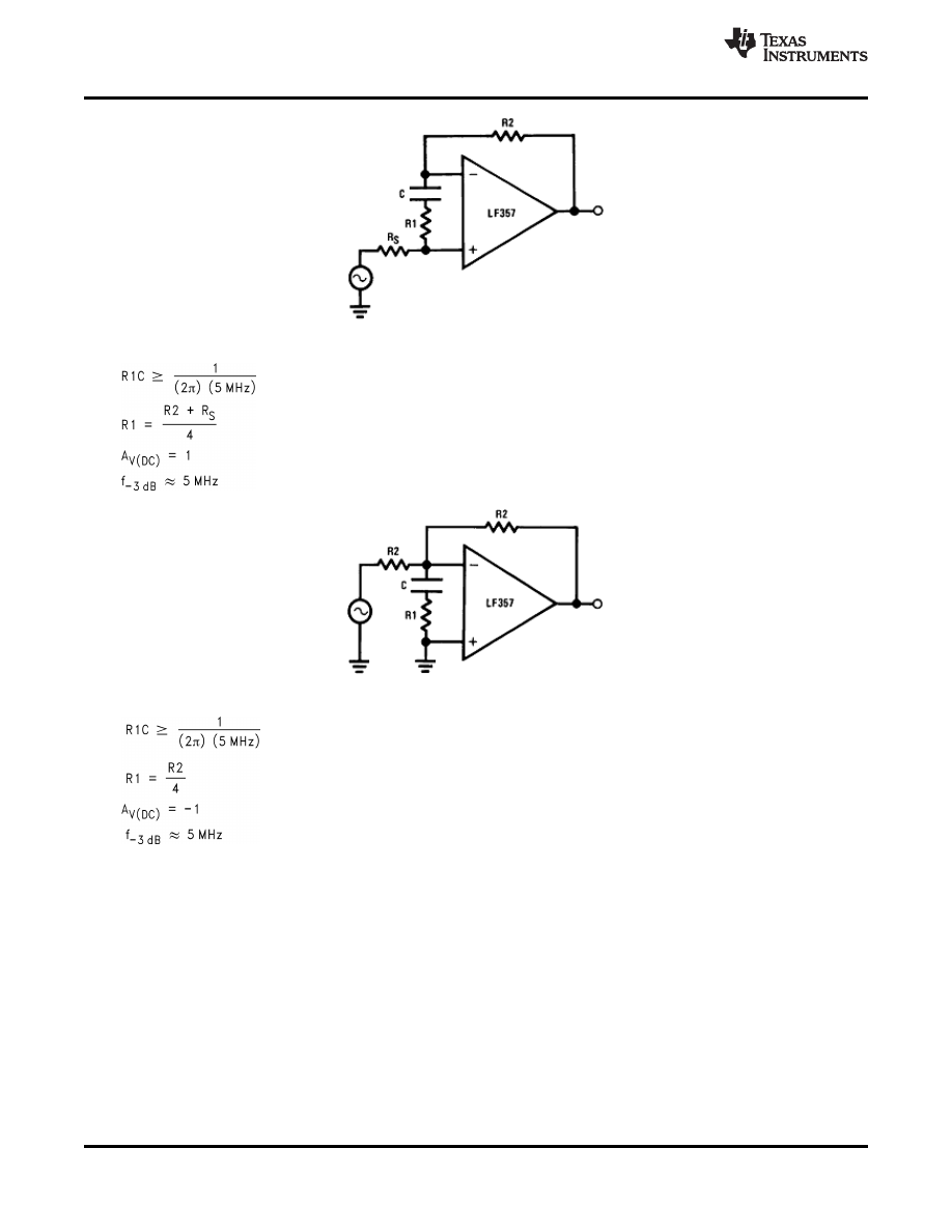
Figure 48. Noninverting Unity Gain Operation for LF157
(6)
Figure 49. Inverting Unity Gain for LF157
(7)
26
Copyright © 2000-2015, Texas Instruments Incorporated
LF155, , , LF257
LF355, , LF357
SNOSBH0D - MAY 2000 - REVISED NOVEMBER 2015
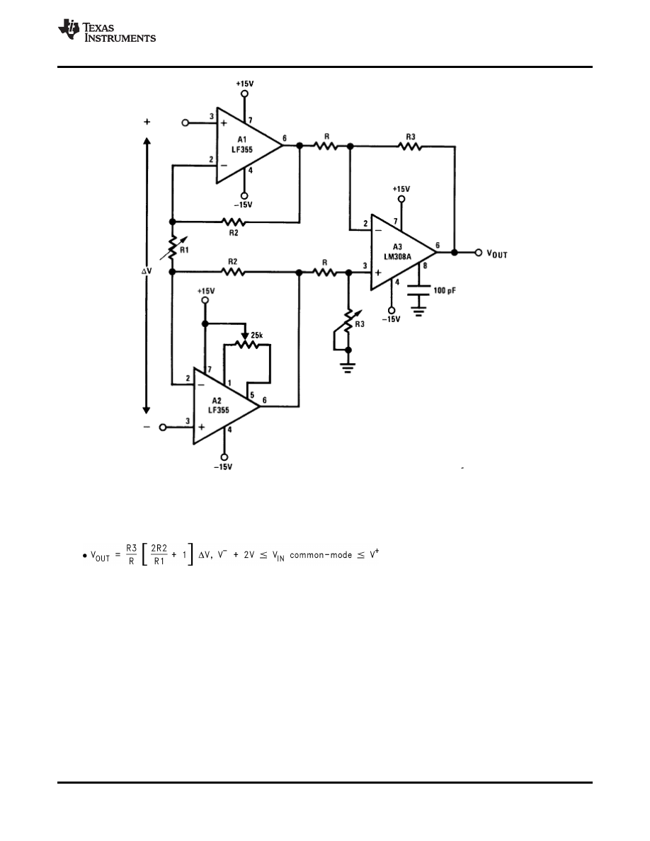
Figure 50. High Impedance, Low Drift Instrumentation Amplifier
System V
OS
adjusted via A2 V
OS
adjust
Trim R3 to boost up CMRR to 120 dB. Instrumentation amplifier resistor array recommended for best
accuracy and lowest drift
(8)
Copyright © 2000-2015, Texas Instruments Incorporated
27
LF155, , LF257
LF355, LF357
SNOSBH0D - MAY 2000 - REVISED NOVEMBER 2015
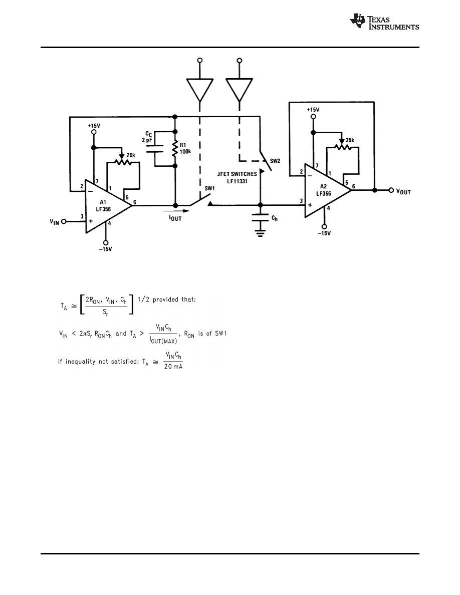
Figure 51. Fast Sample and Hold
Both amplifiers (A1, A2) have feedback loops individually closed with stable responses (overshoot negligible)
Acquisition time T
A
, estimated by:
(9)
LF156 develops full S
r
output capability for V
IN
≥ 1 V
Addition of SW2 improves accuracy by putting the voltage drop across SW1 inside the feedback loop
Overall accuracy of system determined by the accuracy of both amplifiers, A1 and A2
28
Copyright © 2000-2015, Texas Instruments Incorporated
LF155, , , LF257
LF355, , LF357
SNOSBH0D - MAY 2000 - REVISED NOVEMBER 2015
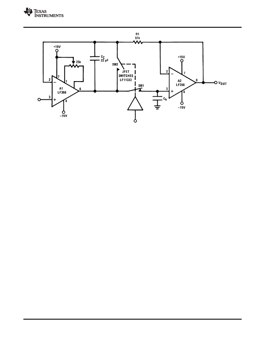
Figure 52. High Accuracy Sample and Hold
By closing the loop through A2, the V
OUT
accuracy will be determined uniquely by A1.
-
No V
OS
adjust required for A2.
T
A
can be estimated by same considerations as previously but, because of the added
-
propagation delay in the feedback loop (A2) the overshoot is not negligible.
Overall system slower than fast sample and hold
R1, C
C
: additional compensation
Use LF156 for
-
Fast settling time
-
Low V
OS
Copyright © 2000-2015, Texas Instruments Incorporated
29
LF155, , LF257
LF355, LF357
SNOSBH0D - MAY 2000 - REVISED NOVEMBER 2015
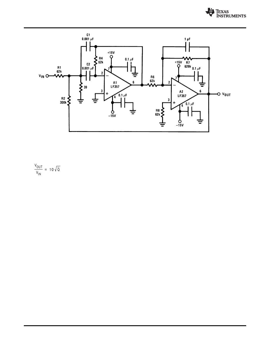
Figure 53. High Q Band Pass Filter
By adding positive feedback (R2)
Q increases to 40
f
BP
= 100 kHz
(10)
Clean layout recommended
Response to a 1-V
p-p
tone burst: 300
μs
30
Copyright © 2000-2015, Texas Instruments Incorporated
LF155, , , LF257
LF355, , LF357
SNOSBH0D - MAY 2000 - REVISED NOVEMBER 2015
Figure 54. High Q Notch Filter
2R1 = R = 10 M
Ω
-
2C = C1 = 300 pF
Capacitors should be matched to obtain high Q
f
NOTCH
= 120 Hz, notch =
-55 dB, Q > 100
Use LF155 for
-
Low I
B
-
Low supply current
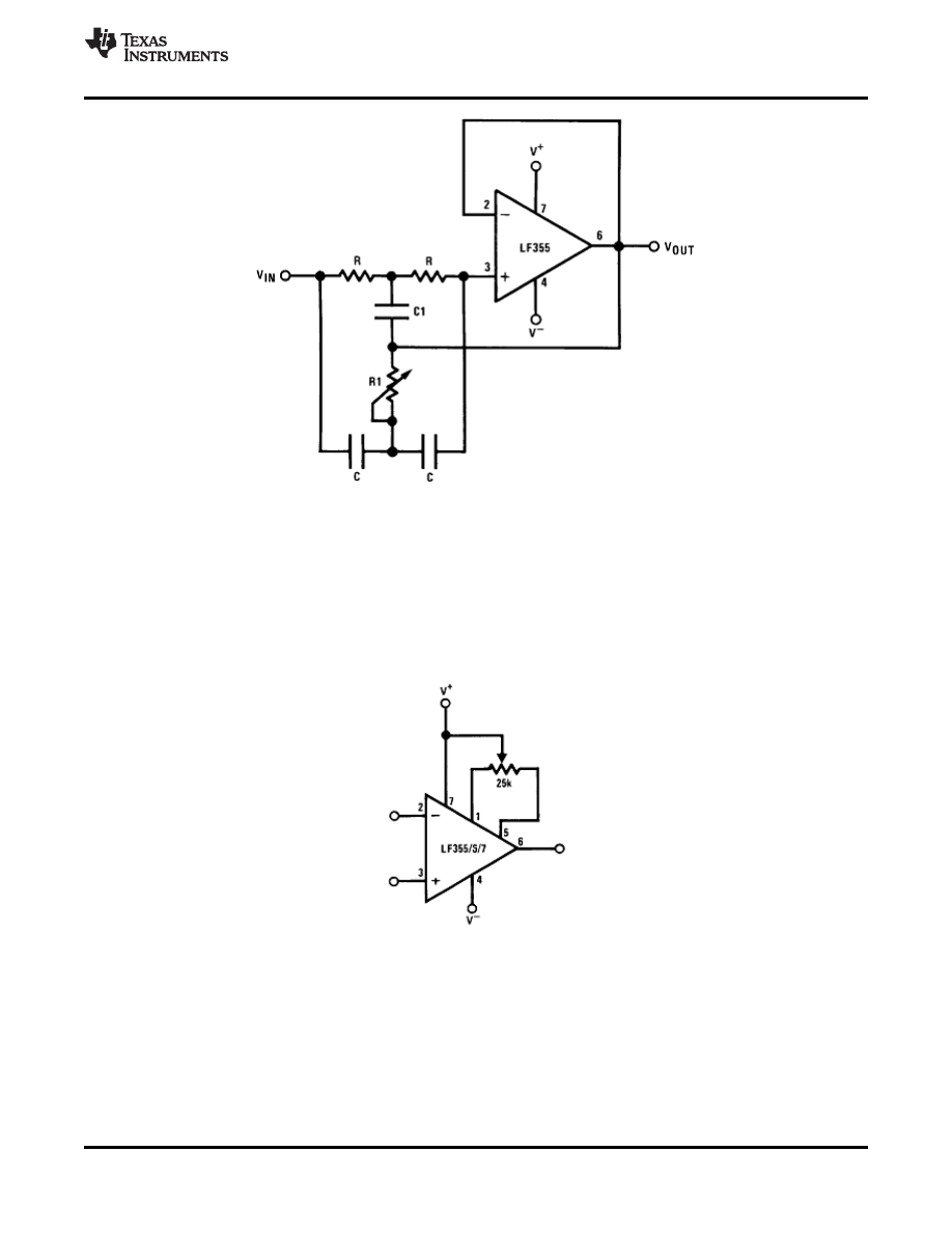
Figure 55. V
OS
Adjustment
V
OS
is adjusted with a 25-k potentiometer
The potentiometer wiper is connected to V
+
For potentiometers with temperature coefficient of 100 ppm/ °C or less the additional drift with adjust
is
0.5 μV/ °C/mV of adjustment
Typical overall drift: 5
μV/ °C ±(0.5 μV/ °C/mV of adj.)
Copyright © 2000-2015, Texas Instruments Incorporated
31
LF155, , LF257
LF355, LF357
SNOSBH0D - MAY 2000 - REVISED NOVEMBER 2015
Figure 56. Driving Capacitive Loads
*
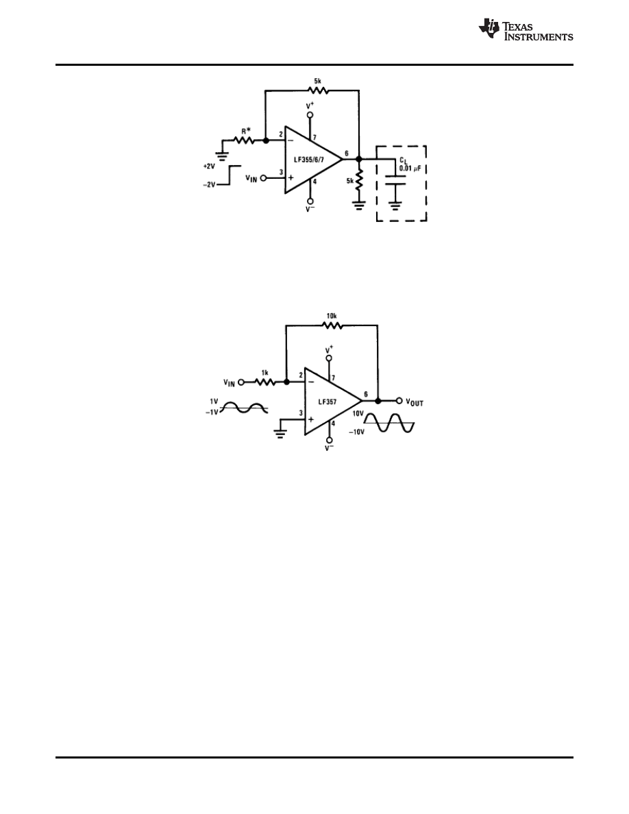
LF15x R = 5k, LF357 R = 1.25 k
Due to a unique output stage design, these amplifiers have the ability to drive large capacitive loads and still
maintain stability. C
L(MAX)
0.01 μF.
Overshoot
≤ 20%, Settling time (t
s
)
5 μs
Figure 57. LF357 - A Large Power BW Amplifier
For distortion
≤ 1% and a 20 Vp-p V
OUT
swing, power bandwidth is: 500 kHz.
32
Copyright © 2000-2015, Texas Instruments Incorporated
LF155, , , LF257
LF355, , LF357
SNOSBH0D - MAY 2000 - REVISED NOVEMBER 2015
9 Power Supply Recommendations
See the
for the minimum and maximum values for the supply input voltage
and operating junction temperature.
10 Layout
10.1 Layout Guidelines
10.1.1 Printed-Circuit-Board Layout For High-Impedance Work
It is generally recognized that any circuit which must operate with less than 1000 pA of leakage current requires
special layout of the PCB. When one wishes to take advantage of the low input bias current of the LFx5x,
typically less than 30 pA, it is essential to have an excellent layout. Fortunately, the techniques of obtaining low
leakages are quite simple. First, the user must not ignore the surface leakage of the PCB, even though it may
sometimes appear acceptably low, because under conditions of high humidity or dust or contamination, the
surface leakage will be appreciable.
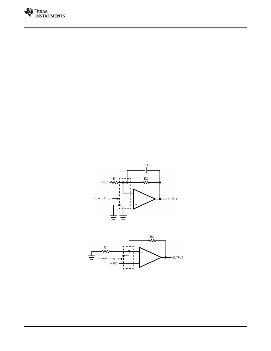
To minimize the effect of any surface leakage, lay out a ring of foil completely surrounding the inputs of the
LFx5x and the terminals of capacitors, diodes, conductors, resistors, relay terminals, and so forth, connected to
the inputs of the op amp, as in
To have a significant effect, guard rings must be placed on both the
top and bottom of the PCB. This PC foil must then be connected to a voltage that is at the same voltage as the
amplifier inputs, because no leakage current can flow between two points at the same potential. For example, a
PCB trace-to-pad resistance of 10 T
Ω, which is normally considered a very large resistance, could leak 5 pA if
the trace were a 5-V bus adjacent to the pad of the input. If a guard ring is used and held close to the potential of
the amplifier inputs, it will significantly reduce this leakage current.
Figure 58. Inverting Amplifier
Figure 59. Noninverting Amplifier
Copyright © 2000-2015, Texas Instruments Incorporated
33
LF155, , LF257
LF355, LF357
SNOSBH0D - MAY 2000 - REVISED NOVEMBER 2015
Layout Guidelines (continued)
Figure 60. Typical Connections Of Guard Rings
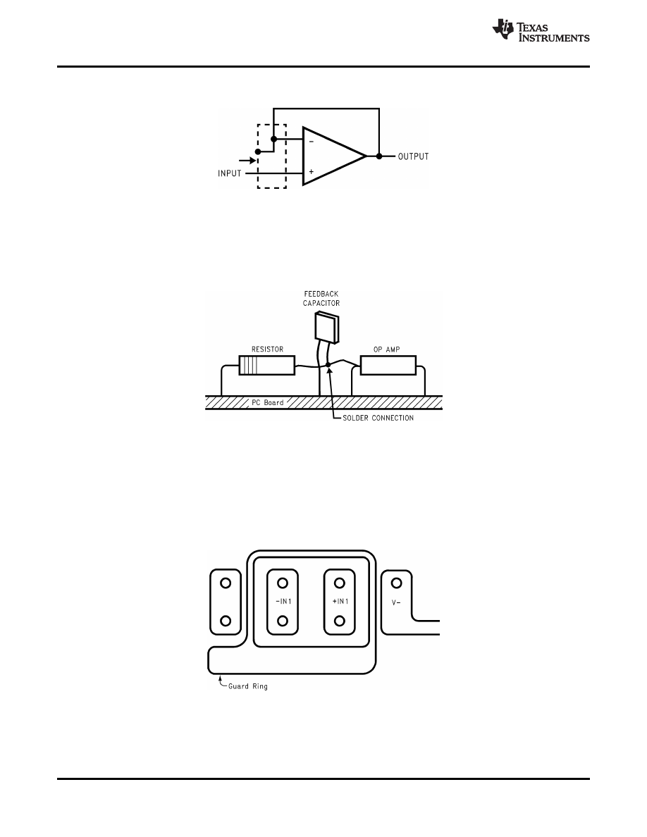
The designer should be aware that when it is inappropriate to lay out a PCB for the sake of just a few circuits,
there is another technique which is even better than a guard ring on a PCB: Do not insert the input pin of the
amplifier into the board at all, but bend it up in the air and use only air as an insulator. Air is an excellent
insulator. In this case you may have to forego some of the advantages of PCB construction, but the advantages
are sometimes well worth the effort of using point-to-point up-in-the-air wiring. See
.
(Input pins are lifted out of PCB and soldered directly to components. All other pins connected to PCB).
Figure 61. Air Wiring
Another potential source of leakage that might be overlooked is the device package. When the LFx5x is
manufactured, the device is always handled with conductive finger cots. This is to assure that salts and skin oils
do not cause leakage paths on the surface of the package. We recommend that these same precautions be
adhered to, during all phases of inspection, test and assembly.
10.2 Layout Example
Figure 62. Examples Of Guard
Ring In PCB Layout
34
Copyright © 2000-2015, Texas Instruments Incorporated
LF155, , , LF257
LF355, , LF357
SNOSBH0D - MAY 2000 - REVISED NOVEMBER 2015
11 Device and Documentation Support
11.1 Related Links
The table below lists quick access links. Categories include technical documents, support and community
resources, tools and software, and quick access to sample or buy.
Table 2. Related Links
TECHNICAL
TOOLS &
SUPPORT &
PARTS
PRODUCT FOLDER
SAMPLE & BUY
DOCUMENTS
SOFTWARE
COMMUNITY
LF156
LF256
LF356
11.2 Community Resources
The following links connect to TI community resources. Linked contents are provided "AS IS" by the respective
contributors. They do not constitute TI specifications and do not necessarily reflect TI's views; see TI's
TI's Engineer-to-Engineer (E2E) Community. Created to foster collaboration
among engineers. At e2e.ti.com, you can ask questions, share knowledge, explore ideas and help
solve problems with fellow engineers.
TI's Design Support Quickly find helpful E2E forums along with design support tools and
contact information for technical support.
11.3 Trademarks
BI-FET, E2E are trademarks of Texas Instruments.
All other trademarks are the property of their respective owners.
11.4 Electrostatic Discharge Caution
These devices have limited built-in ESD protection. The leads should be shorted together or the device placed in conductive foam
during storage or handling to prevent electrostatic damage to the MOS gates.
11.5 Glossary
TI Glossary.
This glossary lists and explains terms, acronyms, and definitions.
12 Mechanical, Packaging, and Orderable Information
The following pages include mechanical, packaging, and orderable information. This information is the most
current data available for the designated devices. This data is subject to change without notice and revision of
this document. For browser-based versions of this data sheet, refer to the left-hand navigation.
Copyright © 2000-2015, Texas Instruments Incorporated
35
PACKAGE OPTION ADDENDUM
www.ti.com
19-Jul-2016
Addendum-Page 1
PACKAGING INFORMATION
Orderable Device
Status
(1)
Package Type Package
Drawing
Pins Package
Qty
Eco Plan
(2)
Lead/Ball Finish
(6)
MSL Peak Temp
(3)
Op Temp ( °C)
Device Marking
(4/5)
Samples
LF156 MD8
ACTIVE
DIESALE
Y
0
204
Green (RoHS
& no Sb/Br)
Call TI
Level-1-NA-UNLIM
-55 to 125
LF156H
ACTIVE
TO-99
LMC
8
500
TBD
Call TI
Call TI
-55 to 125
( LF156H ~ LF156H)
LF156H/NOPB
ACTIVE
TO-99
LMC
8
500
Green (RoHS
& no Sb/Br)
Call TI
Level-1-NA-UNLIM
-55 to 125
( LF156H ~ LF156H)
LF256H
ACTIVE
TO-99
LMC
8
500
TBD
Call TI
Call TI
-25 to 85
( LF256H ~ LF256H)
LF256H/NOPB
ACTIVE
TO-99
LMC
8
500
Green (RoHS
& no Sb/Br)
Call TI
Level-1-NA-UNLIM
-25 to 85
( LF256H ~ LF256H)
LF356 MWC
ACTIVE
WAFERSALE
YS
0
1
Green (RoHS
& no Sb/Br)
Call TI
Level-1-NA-UNLIM
-40 to 85
LF356H
ACTIVE
TO-99
LMC
8
500
TBD
Call TI
Call TI
0 to 70
( LF356H ~ LF356H)
LF356H/NOPB
ACTIVE
TO-99
LMC
8
500
Green (RoHS
& no Sb/Br)
Call TI
Level-1-NA-UNLIM
0 to 70
( LF356H ~ LF356H)
LF356M
NRND
SOIC
D
8
95
TBD
Call TI
Call TI
0 to 70
LF356
M
LF356M/NOPB
ACTIVE
SOIC
D
8
95
Green (RoHS
& no Sb/Br)
CU SN
Level-1-260C-UNLIM
0 to 70
LF356
M
LF356MX
NRND
SOIC
D
8
2500
TBD
Call TI
Call TI
0 to 70
LF356
M
LF356MX/NOPB
ACTIVE
SOIC
D
8
2500
Green (RoHS
& no Sb/Br)
CU SN
Level-1-260C-UNLIM
0 to 70
LF356
M
LF356N/NOPB
ACTIVE
PDIP
P
8
40
Green (RoHS
& no Sb/Br)
CU SN
Level-1-NA-UNLIM
0 to 70
LF
356N
(1)
The marketing status values are defined as follows:
ACTIVE: Product device recommended for new designs.
LIFEBUY: TI has announced that the device will be discontinued, and a lifetime-buy period is in effect.
NRND: Not recommended for new designs. Device is in production to support existing customers, but TI does not recommend using this part in a new design.
PREVIEW: Device has been announced but is not in production. Samples may or may not be available.
OBSOLETE: TI has discontinued the production of the device.
(2)
Eco Plan - The planned eco-friendly classification: Pb-Free (RoHS), Pb-Free (RoHS Exempt), or Green (RoHS & no Sb/Br) - please check
for the latest availability
information and additional product content details.
PACKAGE OPTION ADDENDUM
www.ti.com
19-Jul-2016
Addendum-Page 2
TBD: The Pb-Free/Green conversion plan has not been defined.
Pb-Free (RoHS): TI's terms "Lead-Free" or "Pb-Free" mean semiconductor products that are compatible with the current RoHS requirements for all 6 substances, including the requirement that
lead not exceed 0.1% by weight in homogeneous materials. Where designed to be soldered at high temperatures, TI Pb-Free products are suitable for use in specified lead-free processes.
Pb-Free (RoHS Exempt): This component has a RoHS exemption for either 1) lead-based flip-chip solder bumps used between the die and package, or 2) lead-based die adhesive used between
the die and leadframe. The component is otherwise considered Pb-Free (RoHS compatible) as defined above.
Green (RoHS & no Sb/Br): TI defines "Green" to mean Pb-Free (RoHS compatible), and free of Bromine (Br) and Antimony (Sb) based flame retardants (Br or Sb do not exceed 0.1% by weight
in homogeneous material)
(3)
MSL, Peak Temp. - The Moisture Sensitivity Level rating according to the JEDEC industry standard classifications, and peak solder temperature.
(4)
There may be additional marking, which relates to the logo, the lot trace code information, or the environmental category on the device.
(5)
Multiple Device Markings will be inside parentheses. Only one Device Marking contained in parentheses and separated by a "~" will appear on a device. If a line is indented then it is a continuation
of the previous line and the two combined represent the entire Device Marking for that device.
(6)
Lead/Ball Finish - Orderable Devices may have multiple material finish options. Finish options are separated by a vertical ruled line. Lead/Ball Finish values may wrap to two lines if the finish
value exceeds the maximum column width.
Important Information and Disclaimer:The information provided on this page represents TI's knowledge and belief as of the date that it is provided. TI bases its knowledge and belief on information
provided by third parties, and makes no representation or warranty as to the accuracy of such information. Efforts are underway to better integrate information from third parties. TI has taken and
continues to take reasonable steps to provide representative and accurate information but may not have conducted destructive testing or chemical analysis on incoming materials and chemicals.
TI and TI suppliers consider certain information to be proprietary, and thus CAS numbers and other limited information may not be available for release.
In no event shall TI's liability arising out of such information exceed the total purchase price of the TI part(s) at issue in this document sold by TI to Customer on an annual basis.
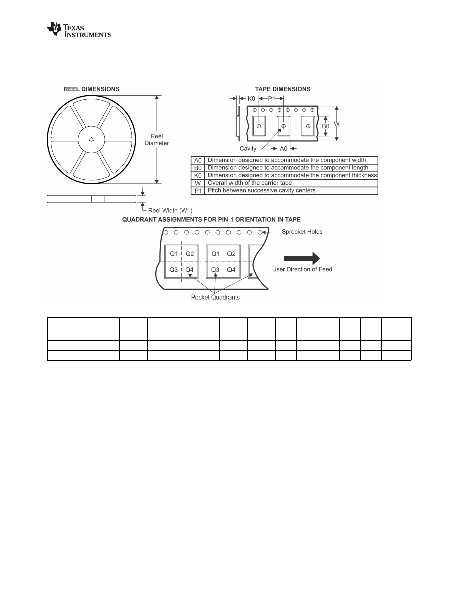
TAPE AND REEL INFORMATION
*All dimensions are nominal
Device
Package
Type
Package
Drawing
Pins
SPQ
Reel
Diameter
(mm)
Reel
Width
W1 (mm)
A0
(mm)
B0
(mm)
K0
(mm)
P1
(mm)
W
(mm)
Pin1
Quadrant
LF356MX
SOIC
D
8
2500
330.0
12.4
6.5
5.4
2.0
8.0
12.0
Q1
LF356MX/NOPB
SOIC
D
8
2500
330.0
12.4
6.5
5.4
2.0
8.0
12.0
Q1
PACKAGE MATERIALS INFORMATION
www.ti.com
10-Aug-2015
Pack Materials-Page 1
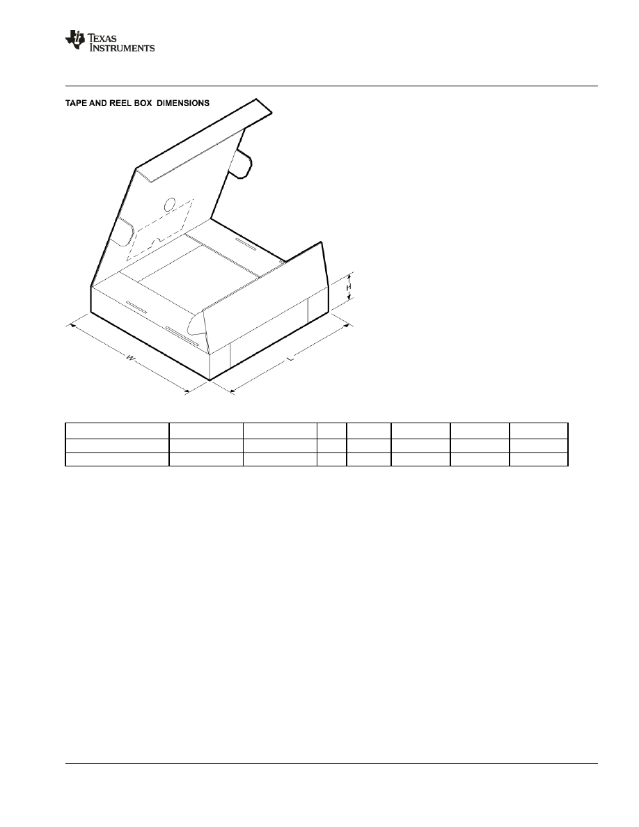
*All dimensions are nominal
Device
Package Type
Package Drawing
Pins
SPQ
Length (mm)
Width (mm)
Height (mm)
LF356MX
SOIC
D
8
2500
367.0
367.0
35.0
LF356MX/NOPB
SOIC
D
8
2500
367.0
367.0
35.0
PACKAGE MATERIALS INFORMATION
www.ti.com
10-Aug-2015
Pack Materials-Page 2

IMPORTANT NOTICE
Texas Instruments Incorporated and its subsidiaries (TI) reserve the right to make corrections, enhancements, improvements and other
changes to its semiconductor products and services per JESD46, latest issue, and to discontinue any product or service per JESD48, latest
issue. Buyers should obtain the latest relevant information before placing orders and should verify that such information is current and
complete. All semiconductor products (also referred to herein as components) are sold subject to TIs terms and conditions of sale
supplied at the time of order acknowledgment.
TI warrants performance of its components to the specifications applicable at the time of sale, in accordance with the warranty in TIs terms
and conditions of sale of semiconductor products. Testing and other quality control techniques are used to the extent TI deems necessary
to support this warranty. Except where mandated by applicable law, testing of all parameters of each component is not necessarily
performed.
TI assumes no liability for applications assistance or the design of Buyers products. Buyers are responsible for their products and
applications using TI components. To minimize the risks associated with Buyers products and applications, Buyers should provide
adequate design and operating safeguards.
TI does not warrant or represent that any license, either express or implied, is granted under any patent right, copyright, mask work right, or
other intellectual property right relating to any combination, machine, or process in which TI components or services are used. Information
published by TI regarding third-party products or services does not constitute a license to use such products or services or a warranty or
endorsement thereof. Use of such information may require a license from a third party under the patents or other intellectual property of the
third party, or a license from TI under the patents or other intellectual property of TI.
Reproduction of significant portions of TI information in TI data books or data sheets is permissible only if reproduction is without alteration
and is accompanied by all associated warranties, conditions, limitations, and notices. TI is not responsible or liable for such altered
documentation. Information of third parties may be subject to additional restrictions.
Resale of TI components or services with statements different from or beyond the parameters stated by TI for that component or service
voids all express and any implied warranties for the associated TI component or service and is an unfair and deceptive business practice.
TI is not responsible or liable for any such statements.
Buyer acknowledges and agrees that it is solely responsible for compliance with all legal, regulatory and safety-related requirements
concerning its products, and any use of TI components in its applications, notwithstanding any applications-related information or support
that may be provided by TI. Buyer represents and agrees that it has all the necessary expertise to create and implement safeguards which
anticipate dangerous consequences of failures, monitor failures and their consequences, lessen the likelihood of failures that might cause
harm and take appropriate remedial actions. Buyer will fully indemnify TI and its representatives against any damages arising out of the use
of any TI components in safety-critical applications.
In some cases, TI components may be promoted specifically to facilitate safety-related applications. With such components, TIs goal is to
help enable customers to design and create their own end-product solutions that meet applicable functional safety standards and
requirements. Nonetheless, such components are subject to these terms.
No TI components are authorized for use in FDA Class III (or similar life-critical medical equipment) unless authorized officers of the parties
have executed a special agreement specifically governing such use.
Only those TI components which TI has specifically designated as military grade or enhanced plastic are designed and intended for use in
military/aerospace applications or environments. Buyer acknowledges and agrees that any military or aerospace use of TI components
which have not been so designated is solely at the Buyer's risk, and that Buyer is solely responsible for compliance with all legal and
regulatory requirements in connection with such use.
TI has specifically designated certain components as meeting ISO/TS16949 requirements, mainly for automotive use. In any case of use of
non-designated products, TI will not be responsible for any failure to meet ISO/TS16949.
Products
Applications
Audio
Automotive and Transportation
Amplifiers
Communications and Telecom
Data Converters
Computers and Peripherals
DLP ® Products
Consumer Electronics
DSP
Energy and Lighting
Clocks and Timers
Industrial
Interface
Medical
Logic
Security
Power Mgmt
Space, Avionics and Defense
Microcontrollers
Video and Imaging
RFID
OMAP Applications Processors
TI E2E Community
Wireless Connectivity
Mailing Address: Texas Instruments, Post Office Box 655303, Dallas, Texas 75265
Copyright © 2016, Texas Instruments Incorporated
Document Outline