| Secciones |
|---|
| Foros Electrónica |
|
|
| Boletines de correo |
 |
OBSOLETE
SNOSBY8D - MAY 1999 - REVISED APRIL 2013
LM12CL 80W Operational Amplifier
Check for Samples:
The turn-on characteristics are controlled by keeping
1
FEATURES
the output open-circuited until the total supply voltage
2
Input Protection
reaches 14V. The output is also opened as the case
Controlled Turn On
temperature exceeds 150 °C or as the supply voltage
approaches the BV
CEO
of the output transistors. The
Thermal Limiting
IC withstands overvoltages to 80V.
Overvoltage Shutdown
This monolithic op amp is compensated for unity-gain
Output-Current Limiting
feedback, with a small-signal bandwidth of 700 kHz.
Dynamic Safe-Area Protection
Slew rate is 9V/
μ
s, even as a follower. Distortion and
capacitive-load stability rival that of the best designs
DESCRIPTION
using complementary output transistors. Further, the
The LM12 is a power op amp capable of driving ±25V
IC withstands large differential input voltages and is
at ±10A while operating from ±30V supplies. The
well behaved should the common-mode range be
monolithic IC can deliver 80W of sine wave power
exceeded.
into
a
4
Ω
load
with
0.01%
distortion.
Power
The LM12 establishes that monolithic ICs can deliver
bandwidth is 60 kHz. Further, a peak dissipation
considerable
output
power
without
resorting
to
capability of 800W allows it to handle reactive loads
complex
switching
schemes.
Devices
can
be
such as transducers, actuators or small motors
paralleled
or
bridged
for
even
greater
output
without derating. Important features include:
capability. Applications include operational power
The IC delivers ±10A output current at any output
supplies, high-voltage regulators, high-quality audio
voltage yet is completely protected against overloads,
amplifiers, tape-head positioners, x-y plotters or other
including shorts to the supplies. The dynamic safe-
servo-control systems.
area protection is provided by instantaneous peak-
The LM12 is supplied in a four-lead, TO-220 package
temperature limiting within the power transistor array.
with V
-
on the case. A gold-eutectic die-attach to a
molybdenum interface is used to avoid thermal
fatigue problems. The LM12 is specified for either
military or commercial temperature range.
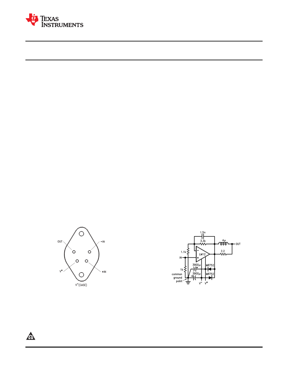
Connection Diagram
Typical Application*
*Low distortion (0.01%) audio amplifier
4-pin glass epoxy TO-3
socket is available from
Figure 1.
AUGAT INC.
Part number 8112-AG7
TO-220
Bottom View
See Package Number NEP
1
Please be aware that an important notice concerning availability, standard warranty, and use in critical applications of
Texas Instruments semiconductor products and disclaimers thereto appears at the end of this data sheet.
2
All trademarks are the property of their respective owners.
PRODUCTION DATA information is current as of publication date.
Copyright © 1999-2013, Texas Instruments Incorporated
Products conform to specifications per the terms of the Texas
Instruments standard warranty. Production processing does not
necessarily include testing of all parameters.
OBSOLETE
SNOSBY8D - MAY 1999 - REVISED APRIL 2013
These devices have limited built-in ESD protection. The leads should be shorted together or the device placed in conductive foam
during storage or handling to prevent electrostatic damage to the MOS gates.
Absolute Maximum Ratings
(1) (2)
Total Supply Voltage
(1)
80V
Input Voltage
See
(3)
Output Current
Internally Limited
Junction Temperature
See
(4)
Storage Temperature Range
-
65 °C to 150 °C
Lead Temperature (Soldering, 10 seconds)
300 °C
(1)
Absolute maximum ratings indicate limits beyond which damage to the device may occur. The maximum voltage for which the LM12 is
ensured to operate is given in the operating ratings and in Note 4. With inductive loads or output shorts, other restrictions described in
applications section apply.
(2)
If Military/Aerospace specified devices are required, please contact the Texas Instruments Sales Office/Distributors for availability and
specifications.
(3)
Neither input should exceed the supply voltage by more than 50 volts nor should the voltage between one input and any other terminal
exceed 60 volts.
(4)
Operating junction temperature is internally limited near 225 °C within the power transistor and 160 °C for the control circuitry.
Operating Ratings
Total Supply Voltage
15V to 60V
Case Temperature
(1)
0 °C to 70 °C
(1)
The supply voltage is ±30V (V
MAX
= 60V), unless otherwise specified. The voltage across the conducting output transistor (supply to
output) is V
DISS
and internal power dissipation is P
DISS
. Temperature range is 0 °C
≤
T
C
≤
70 °C where T
C
is the case temperature.
Standard typeface indicates limits at 25 °C while boldface type refers to limits or special conditions over full temperature range.
With no heat sink, the package will heat at a rate of 35 °C/sec per 100W of internal dissipation.
2
Copyright © 1999-2013, Texas Instruments Incorporated
Product Folder Links:

OBSOLETE
SNOSBY8D - MAY 1999 - REVISED APRIL 2013
Electrical Characteristics
(1)
LM12CL
Typ
Parameter
Conditions
Units
25 °C
Limits
Input Offset Voltage
±10V
≤
V
S
≤
±0.5 V
MAX
, V
CM
= 0
2
15/20
mV (max)
Input Bias Current
V
-
+ 4V
≤
V
CM
≤
V+
-
2V
0.15
0.7/1.0
μ
A (max)
Input Offset Current
V
-
+4V
≤
V
CM
≤
V+
-
2V
0.03
0.2/0.3
μ
A (max)
Common Mode Rejection
V
-
+4V
≤
V
CM
≤
V+
-
2V
86
70/65
dB (min)
Power Supply Rejection
V+ = 0.5 V
MAX
,
90
70/65
dB (min)
-
6V
≥
V
- ≥ -
0.5 V
MAX
V
-
=
-
0.5 V
MAX
,
110
75/70
dB (min)
6V
≤
V+
≤
0.5 V
MAX
Output Saturation Threshold
t
ON
= 1 ms,
Δ
V
IN
= 5 (10 ) mV,
I
OUT
= 1A
1.8
2.2/2.5
V (max)
8A
4
5/7
V (max)
10A
5
V (max)
Large Signal Voltage Gain
t
ON
= 2 ms,
V
SAT
= 2V, I
OUT
= 0
100
30/20
V/mV (min)
V
SAT
= 8V, R
L
= 4
Ω
50
15/10
V/mV (min)
Thermal Gradient Feedback
P
DISS
= 50W, t
ON
= 65 ms
30
100
μ
V/W (max)
Output-Current Limit
t
ON
= 10 ms, V
DISS
= 10V
13
16
A (max)
t
ON
= 100 ms, V
DISS
= 58V
1.5
0.9/0.6
A (min)
1.5
1.7
A (max)
Power Dissipation Rating
t
ON
= 100 ms, V
DISS
= 20V
100
80/55
W (min)
V
DISS
= 58V
80
52/35
W (min)
DC Thermal Resistance
See
(2)
V
DISS
= 20V
2.3
2.9
°C/W (max)
V
DISS
= 58V
2.7
4.5
°C/W (max)
AC Thermal Resistance
See
(2)
1.6
2.1
°C/W (max)
Supply Current
V
OUT
= 0, I
OUT
= 0
60
120/140
mA (max)
(1)
The supply voltage is ±30V (V
MAX
= 60V), unless otherwise specified. The voltage across the conducting output transistor (supply to
output) is V
DISS
and internal power dissipation is P
DISS
. Temperature range is 0 °C
≤
T
C
≤
70 °C where T
C
is the case temperature.
Standard typeface indicates limits at 25 °C while boldface type refers to limits or special conditions over full temperature range.
With no heat sink, the package will heat at a rate of 35 °C/sec per 100W of internal dissipation.
(2)
This thermal resistance is based upon a peak temperature of 200 °C in the center of the power transistor and a case temperature of
25 °C measured at the center of the package bottom. The maximum junction temperature of the control circuitry can be estimated based
upon a dc thermal resistance of 0.9 °C/W or an ac thermal resistance of 0.6 °C/W for any operating voltage.
Copyright © 1999-2013, Texas Instruments Incorporated
3
Product Folder Links:
OBSOLETE
SNOSBY8D - MAY 1999 - REVISED APRIL 2013
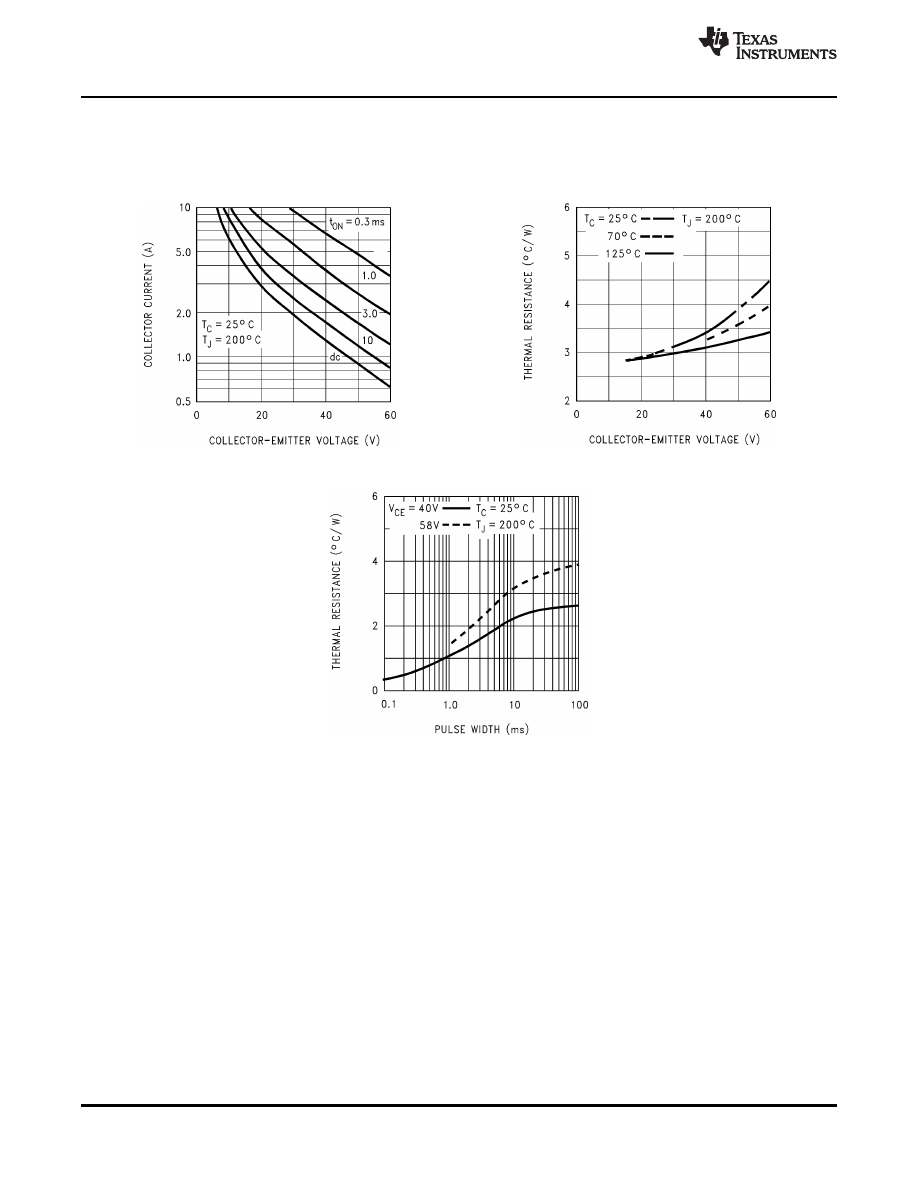
Output-Transistor Ratings (Ensured)
Although the output and supply leads are resistant to electrostatic discharges from handling, the input leads are not. The part
should be treated accordingly.
Safe Area
DC Thermal Resistance
Figure 2.
Figure 3.
Pulse Thermal Resistance
Figure 4.
4
Copyright © 1999-2013, Texas Instruments Incorporated
Product Folder Links:
OBSOLETE
SNOSBY8D - MAY 1999 - REVISED APRIL 2013
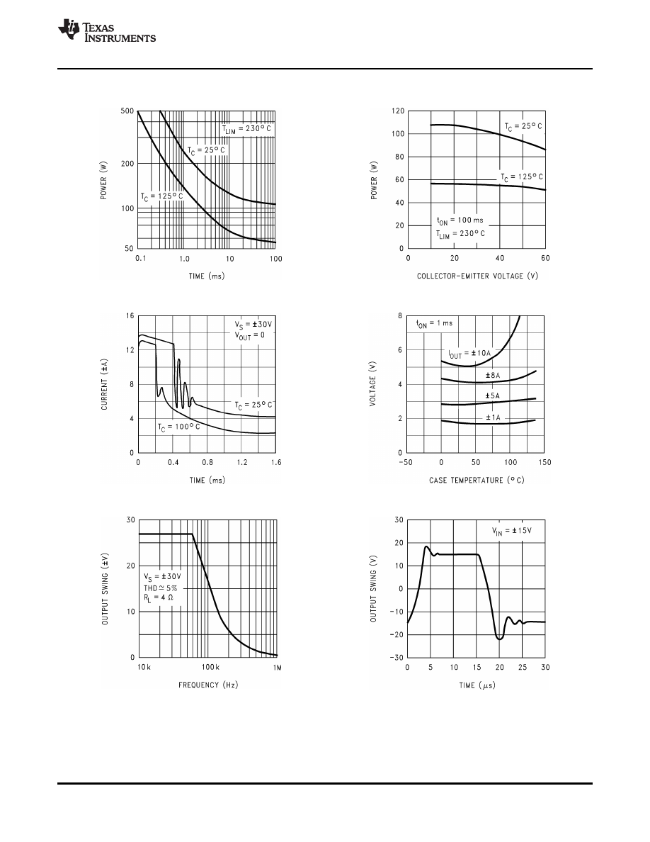
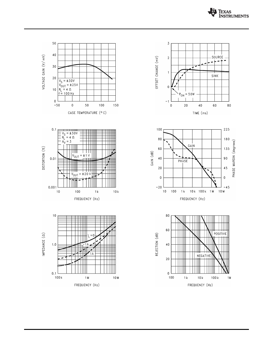
Typical Performance Characteristics
Pulse Power Limit
Pulse Power Limit
Figure 5.
Figure 6.
Peak Output Current
Output Saturation Voltage
Figure 7.
Figure 8.
Large Signal Response
Follower Pulse Response
Figure 9.
Figure 10.
Copyright © 1999-2013, Texas Instruments Incorporated
5
Product Folder Links:
OBSOLETE
SNOSBY8D - MAY 1999 - REVISED APRIL 2013
Typical Performance Characteristics (continued)
Large Signal Gain
Thermal Response
Figure 11.
Figure 12.
Total Harmonic Distortion
Frequency Response
Figure 13.
Figure 14.
Output Impedance
Power Supply Rejection
Figure 15.
Figure 16.
6
Copyright © 1999-2013, Texas Instruments Incorporated
Product Folder Links:
OBSOLETE
SNOSBY8D - MAY 1999 - REVISED APRIL 2013
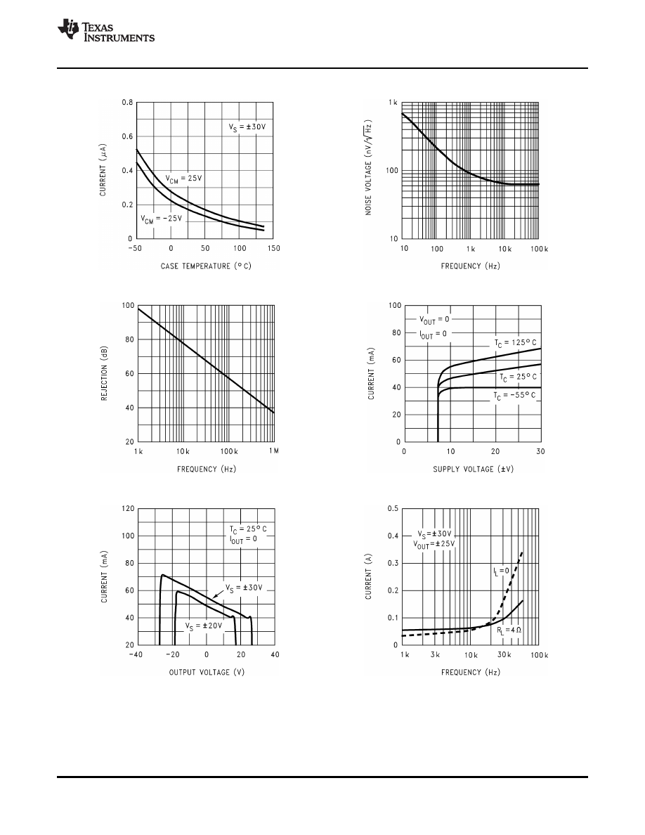
Typical Performance Characteristics (continued)
Input Bias Current
Input Noise Voltage
Figure 17.
Figure 18.
Common Mode Rejection
Supply Current
Figure 19.
Figure 20.
Supply Current
Cross-Supply Current
Figure 21.
Figure 22.
Copyright © 1999-2013, Texas Instruments Incorporated
7
Product Folder Links:

OBSOLETE
SNOSBY8D - MAY 1999 - REVISED APRIL 2013
APPLICATION INFORMATION
GENERAL
Twenty five years ago the operational amplifier was a specialized design tool used primarily for analog
computation. However, the availability of low cost IC op amps in the late 1960's prompted their use in rather
mundane applications, replacing a few discrete components. Once a few basic principles are mastered, op amps
can be used to give exceptionally good results in a wide range of applications while minimizing both cost and
design effort.
The availability of a monolithic power op amp now promises to extend these advantages to high-power designs.
Some conventional applications are given here to illustrate op amp design principles as they relate to power
circuitry. The inevitable fall in prices, as the economies of volume production are realized, will prompt their use in
applications that might now seem trivial. Replacing single power transistors with an op amp will become
economical because of improved performance, simplification of attendant circuitry, vastly improved fault
protection, greater reliability and the reduction of design time.
Power op amps introduce new factors into the design equation. With current transients above 10A, both the
inductance and resistance of wire interconnects become important in a number of ways. Further, power ratings
are a crucial factor in determining performance. But the power capability of the IC cannot be realized unless it is
properly mounted to an adequate heat sink. Thus, thermal design is of major importance with power op amps.
This application summary starts off by identifying the origin of strange problems observed while using the LM12
in a wide variety of designs with all sorts of fault conditions. A few simple precautions will eliminate these
problems. One would do well to read the section on supply bypassing, lead inductance, output clamp
diodes, ground loops and reactive loading before doing any experimentation. Should there be problems
with erratic operation, blow-outs, excessive distortion or oscillation, another look at these sections is in
order.
The management and protection circuitry can also affect operation. Should the total supply voltage exceed
ratings or drop below 15-20V, the op amp shuts off completely. Case temperatures above 150 °C also cause
shut down until the temperature drops to 145 °C. This may take several seconds, depending on the thermal
system. Activation of the dynamic safe-area protection causes both the main feedback loop to lose control and a
reduction in output power, with possible oscillations. In ac applications, the dynamic protection will cause
waveform distortion. Since the LM12 is well protected against thermal overloads, the suggestions for determining
power dissipation and heat sink requirements are presented last.
SUPPLY BYPASSING
All op amps should have their supply leads bypassed with low-inductance capacitors having short leads and
located close to the package terminals to avoid spurious oscillation problems. Power op amps require larger
bypass capacitors. The LM12 is stable with good-quality electrolytic bypass capacitors greater than 20
μ
F. Other
considerations may require larger capacitors.
The current in the supply leads is a rectified component of the load current. If adequate bypassing is not
provided, this distorted signal can be fed back into internal circuitry. Low distortion at high frequencies requires
that the supplies be bypassed with 470
μ
F or more, at the package terminals.
LEAD INDUCTANCE
With ordinary op amps, lead-inductance problems are usually restricted to supply bypassing. Power op amps are
also sensitive to inductance in the output lead, particularly with heavy capacitive loading. Feedback to the input
should be taken directly from the output terminal, minimizing common inductance with the load. Sensing to a
remote load must be accompanied by a high-frequency feedback path directly from the output terminal. Lead
inductance can also cause voltage surges on the supplies. With long leads to the power source, energy stored in
the lead inductance when the output is shorted can be dumped back into the supply bypass capacitors when the
short is removed. The magnitude of this transient is reduced by increasing the size of the bypass capacitor near
the IC. With 20
μ
F local bypass, these voltage surges are important only if the lead length exceeds a couple feet
(> 1
μ
H lead inductance). Twisting together the supply and ground leads minimizes the effect.
8
Copyright © 1999-2013, Texas Instruments Incorporated
Product Folder Links:
OBSOLETE
SNOSBY8D - MAY 1999 - REVISED APRIL 2013
GROUND LOOPS
With fast, high-current circuitry, all sorts of problems can arise from improper grounding. In general, difficulties
can be avoided by returning all grounds separately to a common point. Sometimes this is impractical. When
compromising, special attention should be paid to the ground returns for the supply bypasses, load and input
signal. Ground planes also help to provide proper grounding.
Many problems unrelated to system performance can be traced to the grounding of line-operated test equipment
used for system checkout. Hidden paths are particularly difficult to sort out when several pieces of test equipment
are used but can be minimized by using current probes or the new isolated oscilloscope pre-amplifiers.
Eliminating any direct ground connection between the signal generator and the oscilloscope synchronization
input solves one common problem.
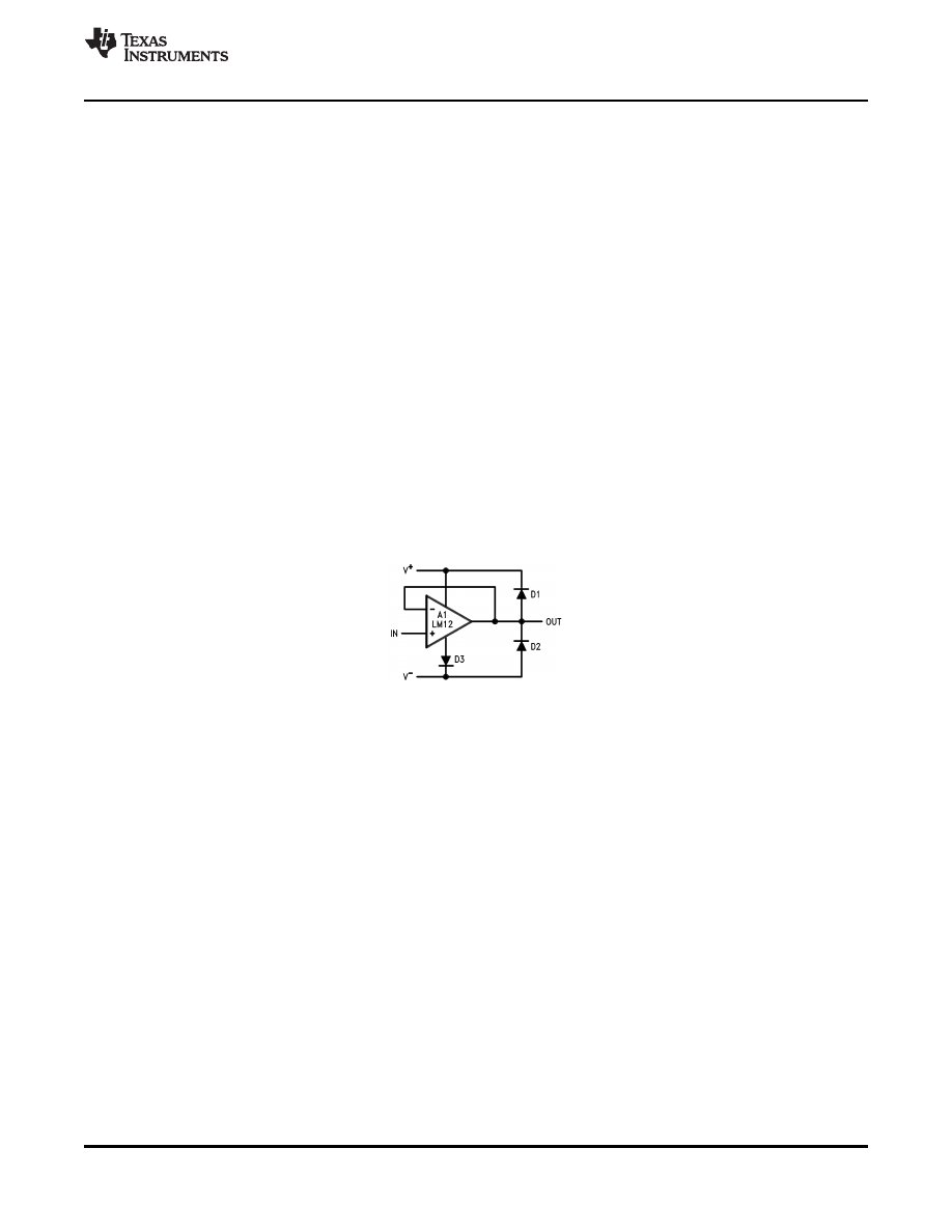
OUTPUT CLAMP DIODES
When a push-pull amplifier goes into power limit while driving an inductive load, the stored energy in the load
inductance can drive the output outside the supplies. Although the LM12 has internal clamp diodes that can
handle several amperes for a few milliseconds, extreme conditions can cause destruction of the IC. The internal
clamp diodes are imperfect in that about half the clamp current flows into the supply to which the output is
clamped while the other half flows across the supplies. Therefore, the use of external diodes to clamp the output
to the power supplies is strongly recommended. This is particularly important with higher supply voltages.
Experience has demonstrated that hard-wire shorting the output to the supplies can induce random failures if
these external clamp diodes are not used and the supply voltages are above ±20V. Therefore it is prudent to use
outputclamp diodes even when the load is not particularly inductive. This also applies to experimental setups in
that blowouts have been observed when diodes were not used. In packaged equipment, it may be possible to
eliminate these diodes, providing that fault conditions can be controlled.
Heat sinking of the clamp diodes is usually unimportant in that they only clamp current transients. Forward drop
with 15A fault transients is of greater concern. Usually, these transients die out rapidly. The clamp to the
negative supply can have somewhat reduced effectiveness under worst case conditions should the forward drop
exceed 1.0V. Mounting this diode to the power op amp heat sink improves the situation. Although the need has
only been demonstrated with some motor loads, including a third diode (D3 above) will eliminate any concern
about the clamp diodes. This diode, however, must be capable of dissipating continuous power as determined by
the negative supply current of the op amp.
Copyright © 1999-2013, Texas Instruments Incorporated
9
Product Folder Links:
OBSOLETE
SNOSBY8D - MAY 1999 - REVISED APRIL 2013
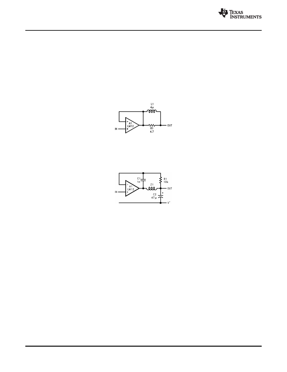
REACTIVE LOADING
The LM12 is normally stable with resistive, inductive or smaller capacitive loads. Larger capacitive loads interact
with the open-loop output resistance (about 1
Ω
) to reduce the phase margin of the feedback loop, ultimately
causing oscillation. The critical capacitance depends upon the feedback applied around the amplifier; a unity-gain
follower can handle about 0.01
μ
F, while more than 1
μ
F does not cause problems if the loop gain is ten. With
loop gains greater than unity, a speedup capacitor across the feedback resistor will aid stability. In all cases, the
op amp will behave predictably only if the supplies are properly bypassed, ground loops are controlled and high-
frequency feedback is derived directly from the output terminal, as recommended earlier.
So-called capacitive loads are not always capacitive. A high-Q capacitor in combination with long leads can
present a series-resonant load to the op amp. In practice, this is not usually a problem; but the situation should
be kept in mind.
Large capacitive loads (including series-resonant) can be accommodated by isolating the feedback amplifier from
the load as shown above. The inductor gives low output impedance at lower frequencies while providing an
isolating impedance at high frequencies. The resistor kills the Q of series resonant circuits formed by capacitive
loads. A low inductance, carbon-composition resistor is recommended. Optimum values of L and R depend upon
the feedback gain and expected nature of the load, but are not critical. A 4
μ
H inductor is obtained with 14 turns
of number 18 wire, close spaced, around a one-inch-diameter form.
The LM12 can be made stable for all loads with a large capacitor on the output, as shown above. This
compensation gives the lowest possible closed-loop output impedance at high frequencies and the best load-
transient response. It is appropriate for such applications as voltage regulators.
A feedback capacitor, C
1
, is connected directly to the output pin of the IC. The output capacitor, C
2
, is connected
at the output terminal with short leads. Single-point grounding to avoid dc and ac ground loops is advised.
The impedance, Z
1
, is the wire connecting the op amp output to the load capacitor. About 3-inches of number-18
wire (70 nH) gives good stability and 18-inches (400 nH) begins to degrade load-transient response. The
minimum load capacitance is 47
μ
F, if a solid-tantalum capacitor with an equivalent series resistance (ESR) of
0.1
Ω
is used. Electrolytic capacitors work as well, although capacitance may have to be increased to 200
μ
F to
bring ESR below 0.1
Ω
.
Loop stability is not the only concern when op amps are operated with reactive loads. With time-varying signals,
power dissipation can also increase markedly. This is particularly true with the combination of capacitive loads
and high-frequency excitation.
10
Copyright © 1999-2013, Texas Instruments Incorporated
Product Folder Links:
OBSOLETE
SNOSBY8D - MAY 1999 - REVISED APRIL 2013
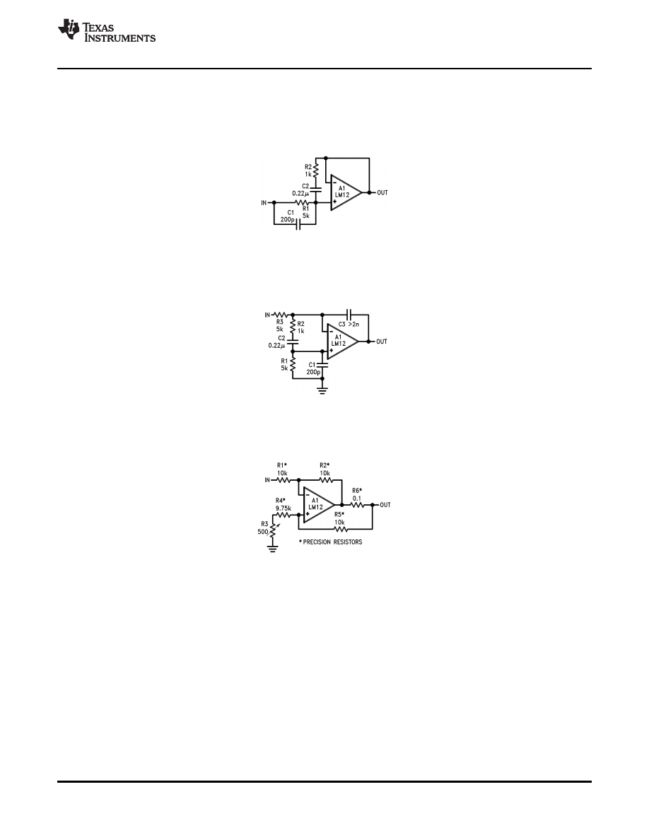
INPUT COMPENSATION
The LM12 is prone to low-amplitude oscillation bursts coming out of saturation if the high-frequency loop gain is
near unity. The voltage follower connection is most susceptible. This glitching can be eliminated at the expense
of small-signal bandwidth using input compensation. Input compensation can also be used in combination with
LR load isolation to improve capacitive load stability.
An example of a voltage follower with input compensation is shown here. The R
2
C
2
combination across the input
works with R
1
to reduce feedback at high frequencies without greatly affecting response below 100 kHz. A lead
capacitor, C
1
, improves phase margin at the unity-gain crossover frequency. Proper operation requires that the
output impedance of the circuitry driving the follower be well under 1 k
Ω
at frequencies up to a few hundred
kilohertz.
Extending input compensation to the integrator connection is shown here. Both the follower and this integrator
will handle 1
μ
F capacitive loading without LR output isolation.
CURRENT DRIVE
This circuit provides an output current proportional to the input voltage. Current drive is sometimes preferred for
servo motors because it aids in stabilizing the servo loop by reducing phase lag caused by motor inductance. In
applications requiring high output resistance, such as operational power supplies running in the current mode,
matching of the feedback resistors to 0.01% is required. Alternately, an adjustable resistor can be used for
trimming.
Copyright © 1999-2013, Texas Instruments Incorporated
11
Product Folder Links:
OBSOLETE
SNOSBY8D - MAY 1999 - REVISED APRIL 2013
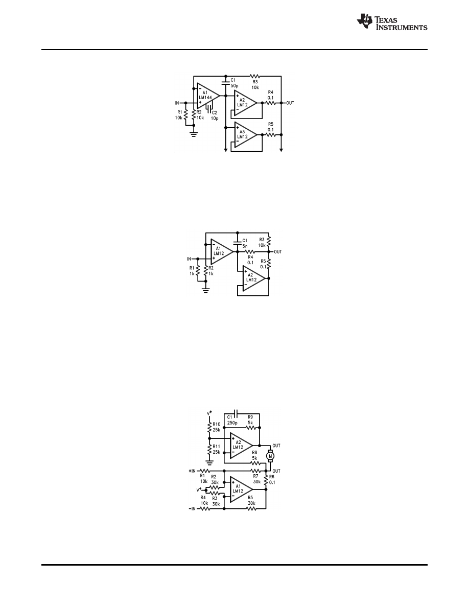
PARALLEL OPERATION
Output drive beyond the capability of one power amplifier can be provided as shown here. The power op amps
are wired as followers and connected in parallel with the outputs coupled through equalization resistors. A
standard, high-voltage op amp is used to provide voltage gain. Overall feedback compensates for the voltage
dropped across the equalization resistors.
With parallel operation, there may be an increase in unloaded supply current related to the offset voltage across
the equalization resistors. More output buffers, with individual equalization resistors, may be added to meet even
higher drive requirements.
This connection allows increased output capability without requiring a separate control amplifier. The output
buffer, A
2
, provides load current through R
5
equal to that supplied by the main amplifier, A
1
, through R
4
. Again,
more output buffers can be added.
Current sharing among paralleled amplifiers can be affected by gain error as the power-bandwidth limit is
approached. In the first circuit, the operating current increase will depend upon the matching of high-frequency
characteristics. In the second circuit, however, the entire input error of A
2
appears across R
4
and R
5
. The supply
current increase can cause power limiting to be activated as the slew limit is approached. This will not damage
the LM12. It can be avoided in both cases by connecting A
1
as an inverting amplifier and restricting bandwidth
with C
1
.
SINGLE-SUPPLY OPERATION
Although op amps are usually operated from dual supplies, single-supply operation is practical. This bridge
amplifier supplies bi-directional current drive to a servo motor while operating from a single positive supply. The
output is easily converted to voltage drive by shorting R
6
and connecting R
7
to the output of A
2
, rather than A
1
.
12
Copyright © 1999-2013, Texas Instruments Incorporated
Product Folder Links:
OBSOLETE
SNOSBY8D - MAY 1999 - REVISED APRIL 2013
Either input may be grounded, with bi-directional drive provided to the other. It is also possible to connect one
input to a positive reference, with the input signal varying about this voltage. If the reference voltage is above 5V,
R
2
and R
3
are not required.
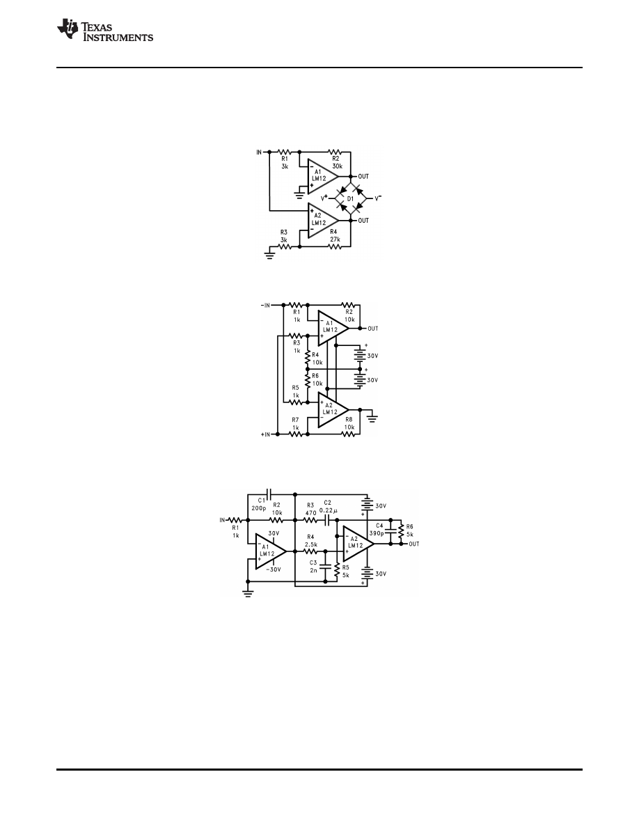
HIGH VOLTAGE AMPLIFIERS
The voltage swing delivered to the load can be doubled by using the bridge connection shown here. Output
clamping to the supplies can be provided by using a bridge-rectifier assembly.
One limitation of the standard bridge connection is that the load cannot be returned to ground. This can be
circumvented by operating the bridge with floating supplies, as shown above. For single-ended drive, either input
can be grounded.
This circuit shows how two amplifiers can be cascaded to double output swing. The advantage over the bridge is
that the output can be increased with any number of stages, although separate supplies are required for each.
Copyright © 1999-2013, Texas Instruments Incorporated
13
Product Folder Links:
OBSOLETE
SNOSBY8D - MAY 1999 - REVISED APRIL 2013
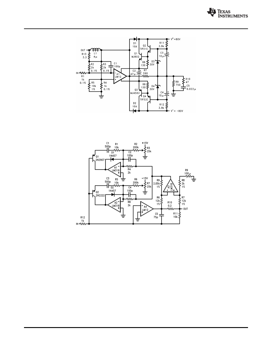
Discrete transistors can be used to increase output drive to ±70V at ±10A as shown above. With proper thermal
design, the IC will provide safe-area protection for the external transistors. Voltage gain is about thirty.
OPERATIONAL POWER SUPPLY
Note: Supply voltages for the LM318s are ±15V
External current limit can be provided for a power op amp as shown above. The positive and negative current
limits can be set precisely and independently. Fast response is assured by D
1
and D
2
. Adjustment range can be
set down to zero with potentiometers R
3
and R
7
. Alternately, the limit can be programmed from a voltage
supplied to R
2
and R
6
. This is the set up required for an operational power supply or voltage-programmable
power source.
14
Copyright © 1999-2013, Texas Instruments Incorporated
Product Folder Links:
OBSOLETE
SNOSBY8D - MAY 1999 - REVISED APRIL 2013
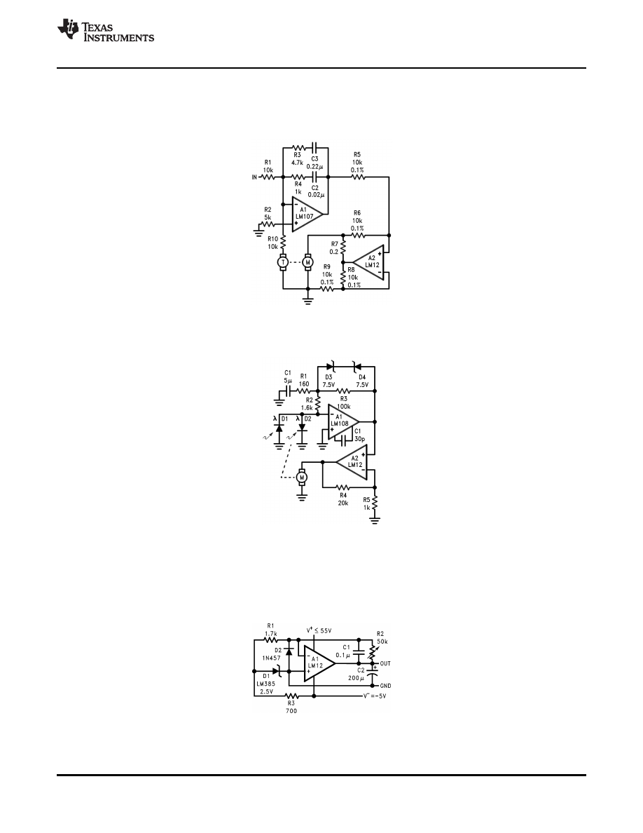
SERVO AMPLIFIERS
When making servo systems with a power op amp, there is a temptation to use it for frequency shaping to
stabilize the servo loop. Sometimes this works; other times there are better ways; and occasionally it just doesn't
fly. Usually it's a matter of how quickly and to what accuracy the servo must stabilize.
This motor/tachometer servo gives an output speed proportional to input voltage. A low-level op amp is used for
frequency shaping while the power op amp provides current drive to the motor. Current drive eliminates loop
phase shift due to motor inductance and makes high-performance servos easier to stabilize.
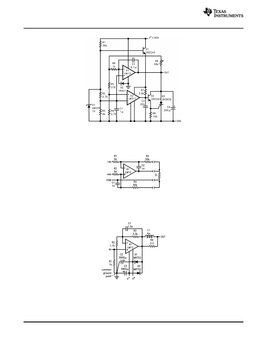
This position servo uses an op amp to develop the rate signal electrically instead of using a tachometer. In high-
performance servos, rate signals must be developed with large error signals well beyond saturation of the motor
drive. Using a separate op amp with a feedback clamp allows the rate signal to be developed properly with
position errors more than an order of magnitude beyond the loop-saturation level as long as the photodiode
sensors are positioned with this in mind.
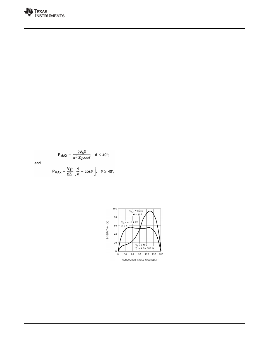
VOLTAGE REGULATORS
An op amp can be used as a positive or negative regulator. Unlike most regulators, it can sink current to absorb
energy dumped back into the output. This positive regulator has a 0-50V output range.
Copyright © 1999-2013, Texas Instruments Incorporated
15
Product Folder Links:
OBSOLETE
SNOSBY8D - MAY 1999 - REVISED APRIL 2013
Dual supplies are not required to use an op amp as a voltage regulator if zero output is not required. This 4V to
50V regulator operates from a single supply. Should the op amp not be able to absorb enough energy to control
an overvoltage condition, a SCR will crowbar the output.
REMOTE SENSING
Remote sensing as shown above allows the op amp to correct for dc drops in cables connecting the load. Even
so, cable drop will affect transient response. Degradation can be minimized by using twisted, heavy-gauge wires
on the output line. Normally, common and one input are connected together at the sending end.
AUDIO AMPLIFIERS
A power amplifier suitable for use in high-quality audio equipment is shown above. Harmonic distortion is about
0.01-percent. Intermodulation distortion (60 Hz/7 kHz, 4:1) measured 0.015-percent. Transient response and
saturation recovery are clean, and the 9 V/
μ
s slew rate of the LM12 virtually eliminates transient intermodulation
distortion. Using separate amplifiers to drive low- and high-frequency speakers gets rid of high-level crossover
networks and attenuators. Further, it prevents clipping on the low-frequency channel from distorting the high
frequencies.
16
Copyright © 1999-2013, Texas Instruments Incorporated
Product Folder Links:
OBSOLETE
SNOSBY8D - MAY 1999 - REVISED APRIL 2013
DETERMINING MAXIMUM DISSIPATION
It is a simple matter to establish power requirements for an op amp driving a resistive load at frequencies well
below 10 Hz. Maximum dissipation occurs when the output is at one-half the supply voltage with high-line
conditions. The individual output transistors must be rated to handle this power continuously at the maximum
expected case temperature. The power rating is limited by the maximum junction temperature as determined by
T
J
= T
C
+ P
DISS
Θ
JC
where
T
C
is the case temperature as measured at the center of the package bottom
P
DISS
is the maximum power dissipation
Θ
JC
is the thermal resistance at the operating voltage of the output transistor
(1)
Recommended maximum junction temperatures are 200 °C within the power transistor and 150 °C for the control
circuitry.
If there is ripple on the supply bus, it is valid to use the average value in worst-case calculations as long as the
peak rating of the power transistor is not exceeded at the ripple peak. With 120 Hz ripple, this is 1.5 times the
continuous power rating.
Dissipation requirements are not so easily established with time varying output signals, especially with reactive
loads. Both peak and continuous dissipation ratings must be taken into account, and these depend on the signal
waveform as well as load characteristics.
With a sine wave output, analysis is fairly straightforward. With supply voltages of ±V
S
, the maximum average
power dissipation of both output transistors is
where
Z
L
is the magnitude of the load impedance
Θ
its phase angle
(2)
Maximum average dissipation occurs below maximum output swing for
Θ
< 40 °.
The instantaneous power dissipation over the conducting half cycle of one output transistor is shown here. Power
dissipation is near zero on the other half cycle. The output level is that resulting in maximum peak and average
dissipation. Plots are given for a resistive and a series RL load. The latter is representative of a 4
Ω
loudspeaker
operating below resonance and would be the worst case condition in most audio applications. The peak
dissipation of each transistor is about four times average. In ac applications, power capability is often limited by
the peak ratings of the power transistor.
Copyright © 1999-2013, Texas Instruments Incorporated
17
Product Folder Links:

OBSOLETE
SNOSBY8D - MAY 1999 - REVISED APRIL 2013
The pulse thermal resistance of the LM12 is specified for constant power pulse duration. Establishing an exact
equivalency between constant-power pulses and those encountered in practice is not easy. However, for sine
waves, reasonable estimates can be made at any frequency by assuming a constant power pulse amplitude
given by:
where
Ï
= 60 °
Θ
is the absolute value of the phase angle of Z
L
(3)
Equivalent pulse width is t
ON
0.4
Ï
for
Θ
= 0 and t
ON
0.2
Ï
for
Θ ≥
20 °, where
Ï
is the period of the output
waveform.
DISSIPATION DRIVING MOTORS
A motor with a locked rotor looks like an inductance in series with a resistance, for purposes of determining
driver dissipation. With slow-response servos, the maximum signal amplitude at frequencies where motor
inductance is significant can be so small that motor inductance does not have to be taken into account. If this is
the case, the motor can be treated as a simple, resistive load as long as the rotor speed is low enough that the
back emf is small by comparison to the supply voltage of the driver transistor.
A permanent-magnet motor can build up a back emf that is equal to the output swing of the op amp driving it.
Reversing this motor from full speed requires the output drive transistor to operate, initially, along a loadline
based upon the motor resistance and total supply voltage. Worst case, this loadline will have to be within the
continuous dissipation rating of the drive transistor; but system dynamics may permit taking advantage of the
higher pulse ratings. Motor inductance can cause added stress if system response is fast.
Shunt- and series-wound motors can generate back emf's that are considerably more than the total supply
voltage, resulting in even higher peak dissipation than a permanent-magnet motor having the same locked-rotor
resistance.
VOLTAGE REGULATOR DISSIPATION
The pass transistor dissipation of a voltage regulator is easily determined in the operating mode. Maximum
continuous dissipation occurs with high line voltage and maximum load current. As discussed earlier, ripple
voltage can be averaged if peak ratings are not exceeded; however, a higher average voltage will be required to
insure that the pass transistor does not saturate at the ripple minimum.
Conditions during start-up can be more complex. If the input voltage increases slowly such that the regulator
does not go into current limit charging output capacitance, there are no problems. If not, load capacitance and
load characteristics must be taken into account. This is also the case if automatic restart is required in recovering
from overloads.
Automatic restart or start-up with fast-rising input voltages cannot be ensured unless the continuous dissipation
rating of the pass transistor is adequate to supply the load current continuously at all voltages below the
regulated output voltage. In this regard, the LM12 performs much better than IC regulators using foldback current
limit, especially with high-line input voltage above 20V.
18
Copyright © 1999-2013, Texas Instruments Incorporated
Product Folder Links:
OBSOLETE
SNOSBY8D - MAY 1999 - REVISED APRIL 2013
POWER LIMITING
Should the power ratings of the LM12 be exceeded, dynamic safe-area protection is activated. Waveforms with
this power limiting are shown for the LM12 driving ±26V at 30 Hz into 3
Ω
in series with 24 mH (
Θ
= 45 °). With an
inductive load, the output clamps to the supplies in power limit, as above. With resistive loads, the output voltage
drops in limit. Behavior with more complex RCL loads is between these extremes.
Secondary thermal limit is activated should the case temperature exceed 150 °C. This thermal limit shuts down
the IC completely (open output) until the case temperature drops to about 145 °C. Recovery may take several
seconds.
POWER SUPPLIES
Power op amps do not require regulated supplies. However, the worst-case output power is determined by the
low-line supply voltage in the ripple trough. The worst-case power dissipation is established by the average
supply voltage with high-line conditions. The loss in power output that can be ensured is the square of the ratio
of these two voltages.
Relatively simple off-line switching power supplies can provide voltage conversion, line isolation and 5-percent
regulation while reducing size and weight.
The regulation against ripple and line variations can provide a substantial increase in the power output that can
be specified under worst-case conditions. In addition, switching power supplies can convert low-voltage power
sources such as automotive batteries up to regulated, dual, high-voltage supplies optimized for powering power
op amps.
HEAT SINKING
A semiconductor manufacturer has no control over heat sink design. Temperature rating can only be based upon
case temperature as measured at the center of the package bottom. With power pulses of longer duration than
100 ms, case temperature is almost entirely dependent on heat sink design and the mounting of the IC to the
heat sink.
The design of heat sink is beyond the scope of this work. Convection-cooled heat sinks are available
commercially, and their manufacturers should be consulted for ratings. The preceding figure is a rough guide for
temperature rise as a function of fin area (both sides) available for convection cooling.
Copyright © 1999-2013, Texas Instruments Incorporated
19
Product Folder Links:

OBSOLETE
SNOSBY8D - MAY 1999 - REVISED APRIL 2013
Proper mounting of the IC is required to minimize the thermal drop between the package and the heat sink. The
heat sink must also have enough metal under the package to conduct heat from the center of the package
bottom to the fins without excessive temperature drop.
A thermal grease such as Wakefield type 120 or Thermalloy Thermacote should be used when mounting the
package to the heat sink. Without this compound, thermal resistance will be no better than 0.5 °C/W, and
probably much worse. With the compound, thermal resistance will be 0.2 °C/W or less, assuming under 0.005
inch combined flatness runout for the package and heat sink. Proper torquing of the mounting bolts is important.
Four to six inch-pounds is recommended.
Should it be necessary to isolate V
-
from the heat sink, an insulating washer is required. Hard washers like
berylium oxide, anodized aluminum and mica require the use of thermal compound on both faces. Two-mil mica
washers are most common, giving about 0.4 °C/W interface resistance with the compound. Silicone-rubber
washers are also available. A 0.5 °C/W thermal resistance is claimed without thermal compound. Experience has
shown that these rubber washers deteriorate and must be replaced should the IC be dismounted.
Isostrate insulating pads for four-lead TO-220 packages are available from Power Devices, Inc. Thermal grease
is not required, and the insulators should not be reused.
Definition of Terms
Input offset voltage: The absolute value of the voltage between the input terminals with the output voltage and
current at zero.
Input bias current: The absolute value of the average of the two input currents with the output voltage and
current at zero.
Input offset current: The absolute value of the difference in the two input currents with the output voltage and
current at zero.
Common-mode rejection: The ratio of the input voltage range to the change in offset voltage between the
extremes.
Supply-voltage rejection: The ratio of the specified supply-voltage change to the change in offset voltage
between the extremes.
Output saturation threshold: The output swing limit for a specified input drive beyond that required for zero
output. It is measured with respect to the supply to which the output is swinging.
Large signal voltage gain: The ratio of the output voltage swing to the differential input voltage required to
drive the output from zero to either swing limit. The output swing limit is the supply voltage less a specified
quasi-saturation voltage. A pulse of short enough duration to minimize thermal effects is used as a
measurement signal.
Thermal gradient feedback: The input offset voltage change caused by thermal gradients generated by
heating of the output transistors, but not the package. This effect is delayed by several milliseconds and
results in increased gain error below 100 Hz.
Output-current limit: The output current with a fixed output voltage and a large input overdrive. The limiting
current drops with time once the protection circuitry is activated.
Power dissipation rating: The power that can be dissipated for a specified time interval without activating the
protection circuitry. For time intervals in excess of 100 ms, dissipation capability is determined by heat
sinking of the IC package rather than by the IC itself.
Thermal resistance: The peak, junction-temperature rise, per unit of internal power dissipation, above the case
temperature as measured at the center of the package bottom. The dc thermal resistance applies when
one output transistor is operating continuously. The ac thermal resistance applies with the output
transistors conducting alternately at a high enough frequency that the peak capability of neither transistor
is exceeded.
Supply current: The current required from the power source to operate the amplifier with the output voltage
and current at zero.
20
Copyright © 1999-2013, Texas Instruments Incorporated
Product Folder Links:
OBSOLETE
SNOSBY8D - MAY 1999 - REVISED APRIL 2013
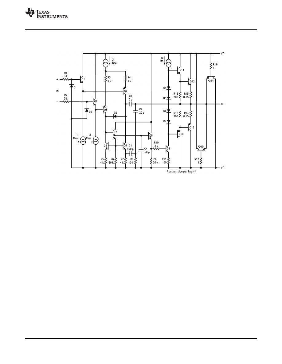
Equivalent Schematic
(excluding active protection circuitry)
Copyright © 1999-2013, Texas Instruments Incorporated
21
Product Folder Links:

OBSOLETE
SNOSBY8D - MAY 1999 - REVISED APRIL 2013
REVISION HISTORY
Changes from Revision C (April 2013) to Revision D
Page
Changed layout of National Data Sheet to TI format ..........................................................................................................
22
Copyright © 1999-2013, Texas Instruments Incorporated
Product Folder Links:

IMPORTANT NOTICE
Texas Instruments Incorporated and its subsidiaries (TI) reserve the right to make corrections, enhancements, improvements and other
changes to its semiconductor products and services per JESD46, latest issue, and to discontinue any product or service per JESD48, latest
issue. Buyers should obtain the latest relevant information before placing orders and should verify that such information is current and
complete. All semiconductor products (also referred to herein as components) are sold subject to TIs terms and conditions of sale
supplied at the time of order acknowledgment.
TI warrants performance of its components to the specifications applicable at the time of sale, in accordance with the warranty in TIs terms
and conditions of sale of semiconductor products. Testing and other quality control techniques are used to the extent TI deems necessary
to support this warranty. Except where mandated by applicable law, testing of all parameters of each component is not necessarily
performed.
TI assumes no liability for applications assistance or the design of Buyers products. Buyers are responsible for their products and
applications using TI components. To minimize the risks associated with Buyers products and applications, Buyers should provide
adequate design and operating safeguards.
TI does not warrant or represent that any license, either express or implied, is granted under any patent right, copyright, mask work right, or
other intellectual property right relating to any combination, machine, or process in which TI components or services are used. Information
published by TI regarding third-party products or services does not constitute a license to use such products or services or a warranty or
endorsement thereof. Use of such information may require a license from a third party under the patents or other intellectual property of the
third party, or a license from TI under the patents or other intellectual property of TI.
Reproduction of significant portions of TI information in TI data books or data sheets is permissible only if reproduction is without alteration
and is accompanied by all associated warranties, conditions, limitations, and notices. TI is not responsible or liable for such altered
documentation. Information of third parties may be subject to additional restrictions.
Resale of TI components or services with statements different from or beyond the parameters stated by TI for that component or service
voids all express and any implied warranties for the associated TI component or service and is an unfair and deceptive business practice.
TI is not responsible or liable for any such statements.
Buyer acknowledges and agrees that it is solely responsible for compliance with all legal, regulatory and safety-related requirements
concerning its products, and any use of TI components in its applications, notwithstanding any applications-related information or support
that may be provided by TI. Buyer represents and agrees that it has all the necessary expertise to create and implement safeguards which
anticipate dangerous consequences of failures, monitor failures and their consequences, lessen the likelihood of failures that might cause
harm and take appropriate remedial actions. Buyer will fully indemnify TI and its representatives against any damages arising out of the use
of any TI components in safety-critical applications.
In some cases, TI components may be promoted specifically to facilitate safety-related applications. With such components, TIs goal is to
help enable customers to design and create their own end-product solutions that meet applicable functional safety standards and
requirements. Nonetheless, such components are subject to these terms.
No TI components are authorized for use in FDA Class III (or similar life-critical medical equipment) unless authorized officers of the parties
have executed a special agreement specifically governing such use.
Only those TI components which TI has specifically designated as military grade or enhanced plastic are designed and intended for use in
military/aerospace applications or environments. Buyer acknowledges and agrees that any military or aerospace use of TI components
which have not been so designated is solely at the Buyer's risk, and that Buyer is solely responsible for compliance with all legal and
regulatory requirements in connection with such use.
TI has specifically designated certain components as meeting ISO/TS16949 requirements, mainly for automotive use. In any case of use of
non-designated products, TI will not be responsible for any failure to meet ISO/TS16949.
Products
Applications
Audio
Automotive and Transportation
Amplifiers
Communications and Telecom
Data Converters
Computers and Peripherals
DLP ® Products
Consumer Electronics
DSP
Energy and Lighting
Clocks and Timers
Industrial
Interface
Medical
Logic
Security
Power Mgmt
Space, Avionics and Defense
Microcontrollers
Video and Imaging
RFID
OMAP Applications Processors
TI E2E Community
Wireless Connectivity
Mailing Address: Texas Instruments, Post Office Box 655303, Dallas, Texas 75265
Copyright © 2013, Texas Instruments Incorporated
Document Outline

