| Secciones |
|---|
| Foros Electrónica |
|
|
| Boletines de correo |
 |
SNAS097C - MAY 1999 - REVISED APRIL 2013
LM1876 Overture™ Audio Power Amplifier Series
Dual 20W Audio Power Amplifier with Mute and Standby Modes
Check for Samples:
1
FEATURES
DESCRIPTION
The LM1876 is a stereo audio amplifier capable of
23
SPiKe Protection
delivering typically 20W per channel of continuous
Minimal Amount of External Components
average output power into a 4
Ω
or 8
Ω
load with less
Necessary
than 0.1% THD+N.
Quiet Fade-In/Out Mute Mode
Each amplifier has an independent smooth transition
Standby-Mode
fade-in/out mute and a power conserving standby
mode which can be controlled by external logic.
Isolated 15-Lead TO-220 Package (PFM)
Non-Isolated 15-lead TO-220 Package
The performance of the LM1876, utilizing its Self
Peak Instantaneous Temperature ( °Ke) ( SPiKe™)
Wide Supply Range 20V - 64V
protection circuitry, places it in a class above discrete
and hybrid amplifiers by providing an inherently,
APPLICATIONS
dynamically protected Safe Operating Area (SOA).
High-End Stereo TVs
SPiKe
protection
means
that
these
parts
are
safeguarded
at
the
output
against
overvoltage,
Component Stereo
undervoltage, overloads, including thermal runaway
Compact Stereo
and instantaneous temperature peaks.
KEY SPECIFICATIONS
THD+N at 1kHz at 2 x 15W continuous
averageoutput power into 4
Ω
or 8
Ω
: 0.1%
(max)
THD+N at 1kHz at continuous average output
power of 2 x 20W into 8
Ω
: 0.009% (typ)
Standby current: 4.2mA (typ)
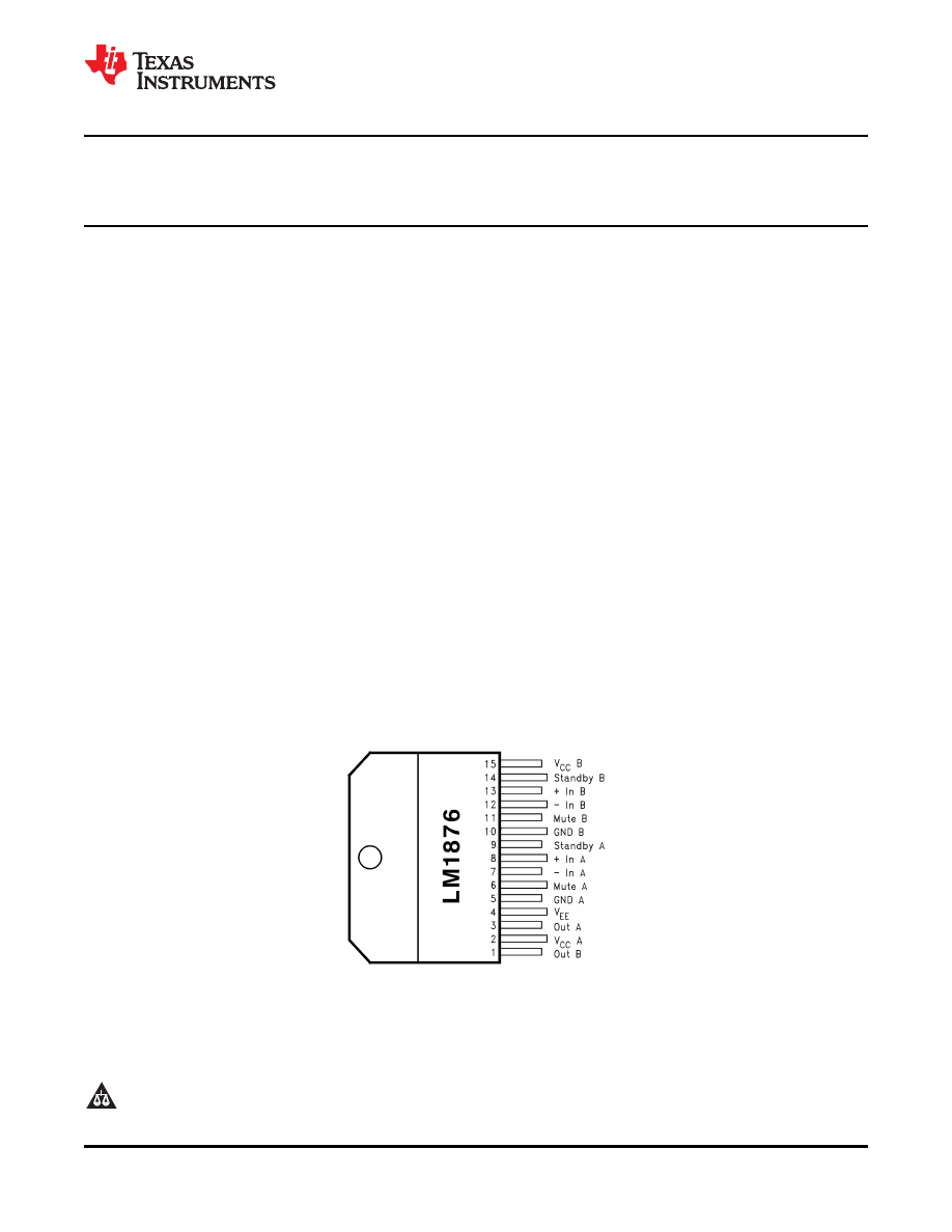
Connection Diagram
Figure 1. Plastic Package- Top View
Isolated Package (PFM)
See Package Number NDB0015B
Non-Isolated Package
See Package Number NDL0015A
1
Please be aware that an important notice concerning availability, standard warranty, and use in critical applications of
Texas Instruments semiconductor products and disclaimers thereto appears at the end of this data sheet.
2
Overture, SPiKe are trademarks of dcl_owner.
3
All other trademarks are the property of their respective owners.
PRODUCTION DATA information is current as of publication date.
Copyright © 1999-2013, Texas Instruments Incorporated
Products conform to specifications per the terms of the Texas
Instruments standard warranty. Production processing does not
necessarily include testing of all parameters.
SNAS097C - MAY 1999 - REVISED APRIL 2013
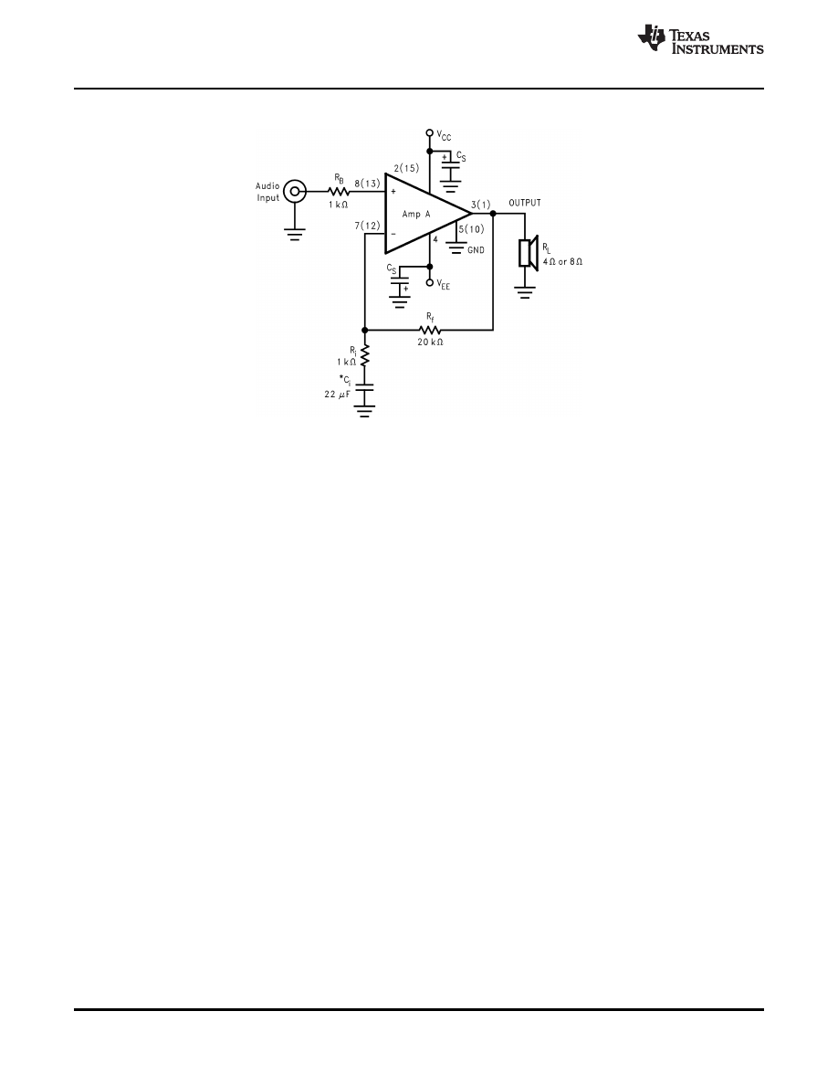
Typical Application
Numbers in parentheses represent pinout for amplifier B.
*Optional component dependent upon specific design requirements.
Figure 2. Typical Audio Amplifier Application Circuit
2
Copyright © 1999-2013, Texas Instruments Incorporated
Product Folder Links:

SNAS097C - MAY 1999 - REVISED APRIL 2013
These devices have limited built-in ESD protection. The leads should be shorted together or the device placed in conductive foam
during storage or handling to prevent electrostatic damage to the MOS gates.
Absolute Maximum Ratings
(1) (2) (3)
Supply Voltage |V
CC
| + |V
EE
| (No Input)
64V
Supply Voltage |V
CC
| + |V
EE
| (with Input)
64V
Common Mode Input Voltage
(V
CC
or V
EE
) and
|V
CC
| + |V
EE
|
≤
54V
Differential Input Voltage
54V
Output Current
Internally Limited
Power Dissipation
(4)
62.5W
ESD Susceptability
(5)
2000V
Junction Temperature
(6)
150 °C
Thermal Resistance
Isolated NDB-Package
Θ
JC
2 °C/W
Non-Isolated NDL-Package
Θ
JC
1 °C/W
Soldering Information
NDB Package (10 sec.)
260 °C
Storage Temperature
-
40 °C to +150 °C
(1)
Absolute Maximum Ratings indicate limits beyond which damage to the device may occur. Operating Ratings indicate conditions for
which the device is functional, but do not ensure specific performance limits. Electrical Characteristics state DC and AC electrical
specifications under particular test conditions which specify performance limits. This assumes that the device is within the Operating
Ratings. Specifications are not ensure for parameters where no limit is given, however, the typical value is a good indication of device
performance.
(2)
All voltages are measured with respect to the GND pins (5, 10), unless otherwise specified.
(3)
If Military/Aerospace specified devices are required, please contact the Texas Instruments Sales Office/ Distributors for availability and
specifications.
(4)
For operating at case temperatures above 25 °C, the device must be derated based on a 150 °C maximum junction temperature and a
thermal resistance of
Θ
JC
= 2 °C/W (junction to case) for the NDB package and
Θ
JC
= 1 °C/W for the NDL package. Refer to
in
(5)
Human body model, 100 pF discharged through a 1.5 k
Ω
resistor.
(6)
The operating junction temperature maximum is 150 °C, however, the instantaneous Safe Operating Area temperature is 250 °C.
Operating Ratings
(1) (2)
Temperature Range
T
MIN
≤
T
A
≤
T
MAX
-
20 °C
≤
T
A
≤
+85 °C
Supply Voltage |V
CC
| + |V
EE
|
(3)
20V to 64V
(1)
All voltages are measured with respect to the GND pins (5, 10), unless otherwise specified.
(2)
Absolute Maximum Ratings indicate limits beyond which damage to the device may occur. Operating Ratings indicate conditions for
which the device is functional, but do not ensure specific performance limits. Electrical Characteristics state DC and AC electrical
specifications under particular test conditions which specify performance limits. This assumes that the device is within the Operating
Ratings. Specifications are not ensure for parameters where no limit is given, however, the typical value is a good indication of device
performance.
(3)
Operation is specified up to 64V, however, distortion may be introduced from SPiKe Protection Circuitry if proper thermal considerations
are not taken into account. Refer to
for a complete explanation.
Copyright © 1999-2013, Texas Instruments Incorporated
3
Product Folder Links:
SNAS097C - MAY 1999 - REVISED APRIL 2013
Electrical Characteristics
(1) (2)
The following specifications apply for V
CC
= +22V, V
EE
=
-
22V with R
L
= 8
Ω
unless otherwise specified. Limits apply for T
A
=
25 °C.
Symbol
Parameter
Conditions
LM1876
Units
(Limits)
Typical
(3
Limit
(4)
)
|V
CC
| +
Power Supply Voltage
(5)
GND
-
V
EE
≥
9V
20
V (min)
|V
EE
|
64
V (max)
P
O
(6)
Output Power
THD + N = 0.1% (max),
(Continuous Average)
f = 1 kHz
|V
CC
| = |V
EE
| = 22V, R
L
= 8
Ω
20
15
W/ch (min)
|V
CC
| = |V
EE
| = 20V, R
L
= 4
Ω
(7)
22
15
W/ch (min)
THD + N
Total Harmonic Distortion
15 W/ch, R
L
= 8
Ω
0.08
%
Plus Noise
15 W/ch, R
L
= 4
Ω
, |V
CC
| = |V
EE
| = 20V
0.1
%
20 Hz
≤
f
≤
20 kHz, A
V
= 26 dB
X
talk
Channel Separation
f = 1 kHz, V
O
= 10.9 Vrms
80
dB
SR
(6)
Slew Rate
V
IN
= 1.414 Vrms, t
rise
= 2 ns
18
12
V/
μ
s (min)
I
total
(8)
Total Quiescent Power
Both Amplifiers V
CM
= 0V,
Supply Current
V
O
= 0V, I
O
= 0 mA
Standby: Off
50
80
mA (max)
Standby: On
4.2
6
mA (max)
V
OS
(8)
Input Offset Voltage
V
CM
= 0V, I
O
= 0 mA
2.0
15
mV (max)
I
B
Input Bias Current
V
CM
= 0V, I
O
= 0 mA
0.2
0.5
μ
A (max)
I
OS
Input Offset Current
V
CM
= 0V, I
O
= 0 mA
0.002
0.2
μ
A (max)
I
O
Output Current Limit
|V
CC
| = |V
EE
| = 10V, t
ON
= 10 ms,
3.5
2.9
Apk (min)
V
O
= 0V
V
OD
(8)
Output Dropout Voltage
(9)
|V
CC
-V
O
|, V
CC
= 20V, I
O
= +100 mA
1.8
2.3
V (max)
|V
O
-V
EE
|, V
EE
=
-
20V, I
O
=
-
100 mA
2.5
3.2
V (max)
PSRR
(8)
Power Supply Rejection Ratio
V
CC
= 25V to 10V, V
EE
=
-
25V,
115
85
dB (min)
V
CM
= 0V, I
O
= 0 mA
V
CC
= 25V, V
EE
=
-
25V to
-
10V
110
85
dB (min)
V
CM
= 0V, I
O
= 0 mA
CMRR
(8)
Common Mode Rejection Ratio
V
CC
= 35V to 10V, V
EE
=
-
10V to
-
35V,
110
80
dB (min)
V
CM
= 10V to
-
10V, I
O
= 0 mA
A
VOL
(8)
Open Loop Voltage Gain
R
L
= 2 k
Ω
,
Δ
V
O
= 20 V
110
90
dB (min)
GBWP
Gain Bandwidth Product
f
O
= 100 kHz, V
IN
= 50 mVrms
7.5
5
MHz (min)
(1)
All voltages are measured with respect to the GND pins (5, 10), unless otherwise specified.
(2)
Absolute Maximum Ratings indicate limits beyond which damage to the device may occur. Operating Ratings indicate conditions for
which the device is functional, but do not ensure specific performance limits. Electrical Characteristics state DC and AC electrical
specifications under particular test conditions which specify performance limits. This assumes that the device is within the Operating
Ratings. Specifications are not ensure for parameters where no limit is given, however, the typical value is a good indication of device
performance.
(3)
Typicals are measured at 25 °C and represent the parametric norm.
(4)
Limits are ensure that all parts are tested in production to meet the stated values.
(5)
V
EE
must have at least
-
9V at its pin with reference to ground in order for the under-voltage protection circuitry to be disabled. In
addition, the voltage differential between V
CC
and V
EE
must be greater than 14V.
(6)
AC Electrical Test; Refer to
(7)
For a 4
Ω
load, and with ±20V supplies, the LM1876 can deliver typically 22W of continuous average output power with less than 0.1%
(THD + N). With supplies above ±20V, the LM1876 cannot deliver more than 22W into a 4
Ω
due to current limiting of the output
transistors. Thus, increasing the power supply above ±20V will only increase the internal power dissipation, not the possible output
power. Increased power dissipation will require a larger heat sink as explained in
(8)
DC Electrical Test; Refer to
.
(9)
The output dropout voltage, V
OD
, is the supply voltage minus the clipping voltage. Refer to
, and
in
.
4
Copyright © 1999-2013, Texas Instruments Incorporated
Product Folder Links:
SNAS097C - MAY 1999 - REVISED APRIL 2013
Electrical Characteristics
(continued)
The following specifications apply for V
CC
= +22V, V
EE
=
-
22V with R
L
= 8
Ω
unless otherwise specified. Limits apply for T
A
=
25 °C.
Symbol
Parameter
Conditions
LM1876
Units
(Limits)
Typical
(3
Limit
(4)
)
e
IN
(6)
Input Noise
IHFA Weighting Filter
2.0
8
μ
V (max)
R
IN
= 600
Ω
(Input Referred)
SNR
Signal-to-Noise Ratio
P
O
= 1W, AWeighted,
98
dB
Measured at 1 kHz, R
S
= 25
Ω
P
O
= 15W, AWeighted
108
dB
Measured at 1 kHz, R
S
= 25
Ω
A
M
Mute Attenuation
Pin 6,11 at 2.5V
115
80
dB (min)
Standby Pin
V
IL
Standby Low Input Voltage
Not in Standby Mode
0.8
V (max)
V
IH
Standby High Input Voltage
In Standby Mode
2.0
2.5
V (min)
Mute pin
V
IL
Mute Low Input Voltage
Outputs Not Muted
0.8
V (max)
V
IH
Mute High Input Voltage
Outputs Muted
2.0
2.5
V (min)
Copyright © 1999-2013, Texas Instruments Incorporated
5
Product Folder Links:
SNAS097C - MAY 1999 - REVISED APRIL 2013
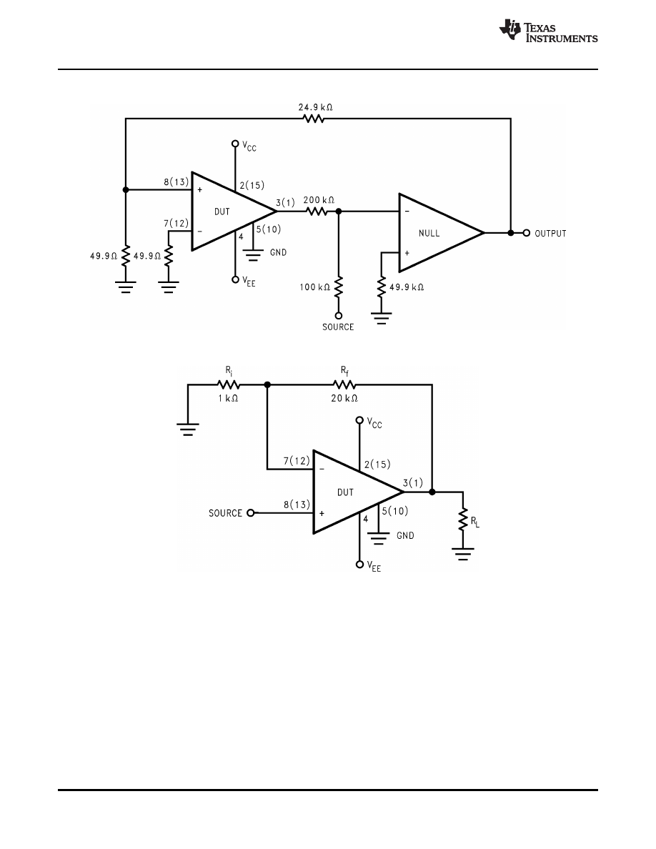
Test Circuit #1 (DC Electrical Test Circuit)
Test Circuit #2 (AC Electrical Test Circuit)
6
Copyright © 1999-2013, Texas Instruments Incorporated
Product Folder Links:
SNAS097C - MAY 1999 - REVISED APRIL 2013
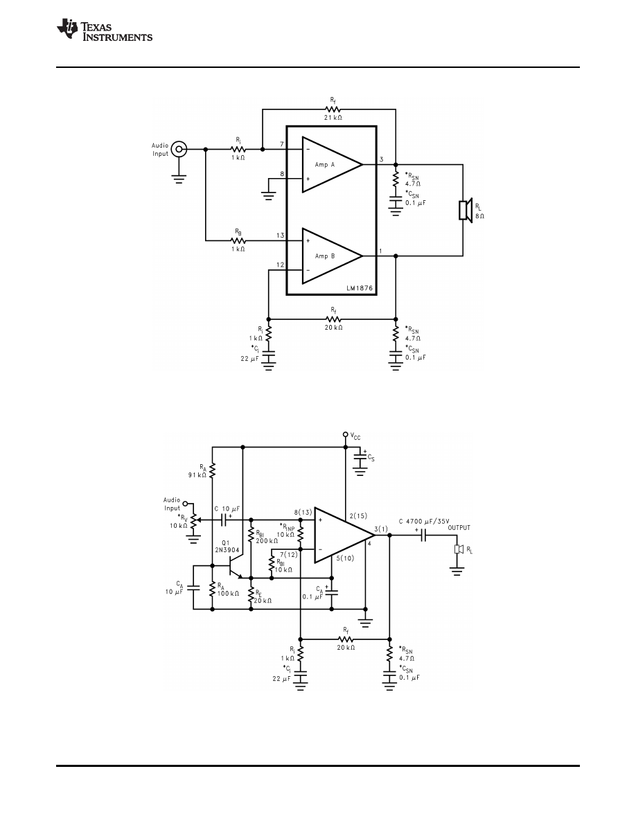
Bridged Amplifier Application Circuit
Figure 3. Bridged Amplifier Application Circuit
Single Supply Application Circuit
*Optional components dependent upon specific design requirements.
Figure 4. Single Supply Amplifier Application Circuit
Copyright © 1999-2013, Texas Instruments Incorporated
7
Product Folder Links:

SNAS097C - MAY 1999 - REVISED APRIL 2013
Auxiliary Amplifier Application Circuit
Figure 5. Special Audio Amplifier Application Circuit
Equivalent Schematic
(excluding active protection circuitry)
Figure 6. LM1876 (per Amp)
8
Copyright © 1999-2013, Texas Instruments Incorporated
Product Folder Links:
SNAS097C - MAY 1999 - REVISED APRIL 2013
(excluding active protection circuitry)
External Components Description
Components
Functional Description
1
R
B
Prevents currents from entering the amplifier's non-inverting input which may be passed through to the load upon
power down of the system due to the low input impedance of the circuitry when the undervoltage circuitry is off.
This phenomenon occurs when the supply voltages are below 1.5V.
2
R
i
Inverting input resistance to provide AC gain in conjunction with R
f
.
3
R
f
Feedback resistance to provide AC gain in conjunction with R
i
.
4
C
i
(1)
Feedback capacitor which ensures unity gain at DC. Also creates a highpass filter with R
i
at f
C
= 1/(2
Ï
R
i
C
i
).
5
C
S
Provides power supply filtering and bypassing. Refer to
for proper placement and selection
of bypass capacitors.
6
R
V
(1)
Acts as a volume control by setting the input voltage level.
7
R
IN
(1)
Sets the amplifier's input terminals DC bias point when C
IN
is present in the circuit. Also works with C
IN
to create a
highpass filter at f
C
= 1/(2
Ï
R
IN
C
IN
). Refer to
8
C
IN
(1)
Input capacitor which blocks the input signal's DC offsets from being passed onto the amplifier's inputs.
9
R
SN
(1)
Works with C
SN
to stabilize the output stage by creating a pole that reduces high frequency instabilities.
10
C
SN
(1)
Works with R
SN
to stabilize the output stage by creating a pole that reduces high frequency instabilities. The pole is
set at f
C
= 1/(2
Ï
R
SN
C
SN
). Refer to
11
L
(1)
Provides high impedance at high frequencies so that R may decouple a highly capacitive load and reduce the Q of
the series resonant circuit. Also provides a low impedance at low frequencies to short out R and pass audio signals
12
R
(1)
to the load. Refer to
.
13
R
A
Provides DC voltage biasing for the transistor Q1 in single supply operation.
14
C
A
Provides bias filtering for single supply operation.
15
R
INP
(1)
Limits the voltage difference between the amplifier's inputs for single supply operation. Refer to
for a more detailed explanation of the function of R
INP
.
16
R
BI
Provides input bias current for single supply operation. Refer to
for a more detailed
explanation of the function of R
BI
.
17
R
E
Establishes a fixed DC current for the transistor Q1 in single supply operation. This resistor stabilizes the half-
supply point along with C
A
.
(1)
Optional components dependent upon specific design requirements.
Copyright © 1999-2013, Texas Instruments Incorporated
9
Product Folder Links:
SNAS097C - MAY 1999 - REVISED APRIL 2013
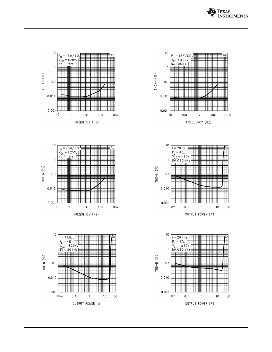
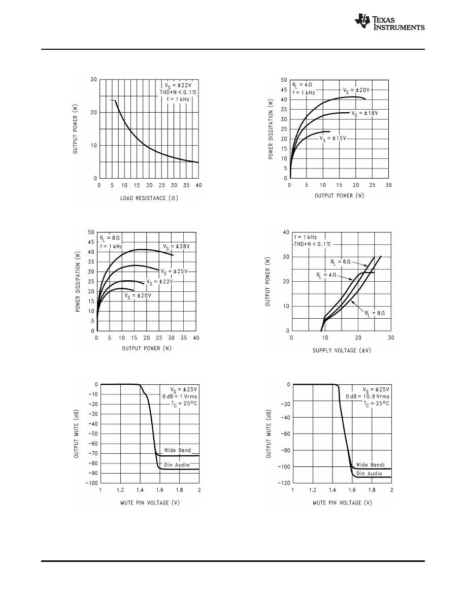
Typical Performance Characteristics
THD + N
THD + N
vs
vs
Frequency
Frequency
Figure 7.
Figure 8.
THD + N
vs
THD + N vs
Frequency
Output Power
Figure 9.
Figure 10.
THD + N vs
THD + N vs
Output Power
Output Power
Figure 11.
Figure 12.
10
Copyright © 1999-2013, Texas Instruments Incorporated
Product Folder Links:

SNAS097C - MAY 1999 - REVISED APRIL 2013
Typical Performance Characteristics (continued)
THD + N vs
THD + N vs
Output Power
Output Power
Figure 13.
Figure 14.
THD + N vs
Clipping Voltage vs
Output Power
Supply Voltage
Figure 15.
Figure 16.
Clipping Voltage vs
Clipping Voltage vs
Supply Voltage
Supply Voltage
Figure 17.
Figure 18.
Copyright © 1999-2013, Texas Instruments Incorporated
11
Product Folder Links:
SNAS097C - MAY 1999 - REVISED APRIL 2013
Typical Performance Characteristics (continued)
Output Power vs
Power Dissipation vs
Load Resistance
Output Power
Figure 19.
Figure 20.
Power Dissipation vs
Output Power vs
Output Power
Supply Voltage
Figure 21.
Figure .
Output Mute vs
Output Mute vs
Mute Pin Voltage
Mute Pin Voltage
Figure 22.
Figure 23.
12
Copyright © 1999-2013, Texas Instruments Incorporated
Product Folder Links:
SNAS097C - MAY 1999 - REVISED APRIL 2013
Typical Performance Characteristics (continued)
Channel Separation vs
Frequency
Pulse Response
Figure 24.
Figure 25.
Power Supply
Large Signal Response
Rejection Ratio
Figure 26.
Figure 27.
Common-Mode
Open Loop
Rejection Ratio
Frequency Response
Figure 28.
Figure 29.
Copyright © 1999-2013, Texas Instruments Incorporated
13
Product Folder Links:
SNAS097C - MAY 1999 - REVISED APRIL 2013
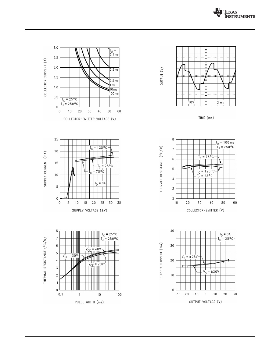
Typical Performance Characteristics (continued)
SPiKe Protection
Safe Area
Response
Figure 30.
Figure 31.
Supply Current vs
Pulse Thermal
Supply Voltage
Resistance
Figure 32.
Figure 33.
Pulse Thermal
Supply Current vs
Resistance
Output Voltage
Figure 34.
Figure 35.
14
Copyright © 1999-2013, Texas Instruments Incorporated
Product Folder Links:
SNAS097C - MAY 1999 - REVISED APRIL 2013
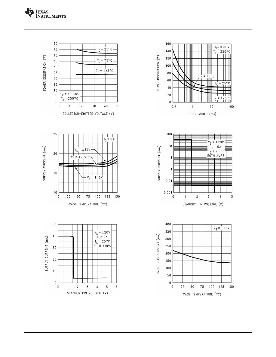
Typical Performance Characteristics (continued)
Pulse Power Limit
Pulse Power Limit
Figure 36.
Figure 37.
Supply Current vs
Supply Current (I
CC
) vs
Case Temperature
Standby Pin Voltage
Figure 38.
Figure 39.
Supply Current (I
EE
) vs
Input Bias Current vs
Standby Pin Voltage
Case Temperature
Figure 40.
Figure 41.
Copyright © 1999-2013, Texas Instruments Incorporated
15
Product Folder Links:

SNAS097C - MAY 1999 - REVISED APRIL 2013
Typical Performance Characteristics (continued)
Output Power/Channel vs
Output Power/Channel vs
Supply Voltage
Supply Voltage
f = 1kHz, R
L
= 4
Ω¦
, 80kHz BW
f = 1kHz, R
L
= 6
Ω¦
, 80kHz BW
Figure 42.
Figure 43.
Output Power/Channel vs
Supply Voltage
f = 1kHz, R
L
= 8
Ω¦
, 80kHz BW
Figure 44.
16
Copyright © 1999-2013, Texas Instruments Incorporated
Product Folder Links:

SNAS097C - MAY 1999 - REVISED APRIL 2013
APPLICATION INFORMATION
MUTE MODE
By placing a logic-high voltage on the mute pins, the signal going into the amplifiers will be muted. If the mute
pins are left floating or connected to a logic-low voltage, the amplifiers will be in a non-muted state. There are
two mute pins, one for each amplifier, so that one channel can be muted without muting the other if the
application requires such a configuration. Refer to
for
and
STANDBY MODE
The standby mode of the LM1876 allows the user to drastically reduce power consumption when the amplifiers
are idle. By placing a logic-high voltage on the standby pins, the amplifiers will go into Standby Mode. In this
mode, the current drawn from the V
CC
supply is typically less than 10
μ
A total for both amplifiers. The current
drawn from the V
EE
supply is typically 4.2 mA. Clearly, there is a significant reduction in idle power consumption
when using the standby mode. There are two Standby pins, so that one channel can be put in standby mode
without putting the other amplifier in standby if the application requires such flexibility. Refer to
for
and
.
UNDER-VOLTAGE PROTECTION
Upon system power-up, the under-voltage protection circuitry allows the power supplies and their corresponding
capacitors to come up close to their full values before turning on the LM1876 such that no DC output spikes
occur. Upon turn-off, the output of the LM1876 is brought to ground before the power supplies such that no
transients occur at power-down.
OVER-VOLTAGE PROTECTION
The LM1876 contains over-voltage protection circuitry that limits the output current to approximately 3.5 Apk
while also providing voltage clamping, though not through internal clamping diodes. The clamping effect is quite
the same, however, the output transistors are designed to work alternately by sinking large current spikes.
SPiKe PROTECTION
The LM1876 is protected from instantaneous peak-temperature stressing of the power transistor array. The
in
shows the area of device operation where SPiKe Protection
Circuitry is not enabled. The waveform to the right of the SOA graph exemplifies how the dynamic protection will
cause waveform distortion when enabled.
THERMAL PROTECTION
The LM1876 has a sophisticated thermal protection scheme to prevent long-term thermal stress of the device.
When the temperature on the die reaches 165 °C, the LM1876 shuts down. It starts operating again when the die
temperature drops to about 155 °C, but if the temperature again begins to rise, shutdown will occur again at
165 °C. Therefore, the device is allowed to heat up to a relatively high temperature if the fault condition is
temporary, but a sustained fault will cause the device to cycle in a Schmitt Trigger fashion between the thermal
shutdown temperature limits of 165 °C and 155 °C. This greatly reduces the stress imposed on the IC by thermal
cycling, which in turn improves its reliability under sustained fault conditions.
Since the die temperature is directly dependent upon the heat sink used, the heat sink should be chosen such
that thermal shutdown will not be reached during normal operation. Using the best heat sink possible within the
cost and space constraints of the system will improve the long-term reliability of any power semiconductor
device, as discussed in
DETERMlNlNG MAXIMUM POWER DISSIPATION
Power dissipation within the integrated circuit package is a very important parameter requiring a thorough
understanding if optimum power output is to be obtained. An incorrect maximum power dissipation calculation
may result in inadequate heat sinking causing thermal shutdown and thus limiting the output power.
Copyright © 1999-2013, Texas Instruments Incorporated
17
Product Folder Links:

SNAS097C - MAY 1999 - REVISED APRIL 2013
exemplifies the theoretical maximum power dissipation point of each amplifier where V
CC
is the total
supply voltage.
P
DMAX
= V
CC
2/2
Ï
2
R
L
(1)
Thus by knowing the total supply voltage and rated output load, the maximum power dissipation point can be
calculated. The package dissipation is twice the number which results from
since there are two
amplifiers in each LM1876. Refer to
and
in
which show
the actual full range of power dissipation not just the maximum theoretical point that results from
DETERMINING THE CORRECT HEAT SINK
The choice of a heat sink for a high-power audio amplifier is made entirely to keep the die temperature at a level
such that the thermal protection circuitry does not operate under normal circumstances.
The thermal resistance from the die (junction) to the outside air (ambient) is a combination of three thermal
resistances,
Θ
JC
,
Θ
CS
, and
Θ
SA
. In addition, the thermal resistance,
Θ
JC
(junction to case), of the LM1876TF is
2 °C/W and the LM1876T is 1 °C/W. Using Thermalloy Thermacote thermal compound, the thermal resistance,
Θ
CS
(case to sink), is about 0.2 °C/W. Since convection heat flow (power dissipation) is analogous to current flow,
thermal resistance is analogous to electrical resistance, and temperature drops are analogous to voltage drops,
the power dissipation out of the LM1876 is equal to the following:
P
DMAX
= (T
JMAX
-
T
AMB
)/
Θ
JA
where
T
JMAX
= 150 °C
T
AMB
is the system ambient temperature
Θ
JA
=
Θ
JC
+
Θ
CS
+
Θ
SA
(2)
Once the maximum package power dissipation has been calculated using
, the maximum thermal
resistance,
Θ
SA
, (heat sink to ambient) in °C/W for a heat sink can be calculated. This calculation is made using
which is derived by solving for
Θ
SA
in
Θ
SA
= [(T
JMAX
-
T
AMB
)
-
P
DMAX
(
Θ
JC
+
Θ
CS
)]/P
DMAX
(3)
Again it must be noted that the value of
Θ
SA
is dependent upon the system designer's amplifier requirements. If
the ambient temperature that the audio amplifier is to be working under is higher than 25 °C, then the thermal
resistance for the heat sink, given all other things are equal, will need to be smaller.
SUPPLY BYPASSING
The LM1876 has excellent power supply rejection and does not require a regulated supply. However, to improve
system performance as well as eliminate possible oscillations, the LM1876 should have its supply leads
bypassed with low-inductance capacitors having short leads that are located close to the package terminals.
Inadequate power supply bypassing will manifest itself by a low frequency oscillation known as motorboating or
by high frequency instabilities. These instabilities can be eliminated through multiple bypassing utilizing a large
tantalum or electrolytic capacitor (10
μ
F or larger) which is used to absorb low frequency variations and a small
ceramic capacitor (0.1
μ
F) to prevent any high frequency feedback through the power supply lines.
If adequate bypassing is not provided, the current in the supply leads which is a rectified component of the load
current may be fed back into internal circuitry. This signal causes distortion at high frequencies requiring that the
supplies be bypassed at the package terminals with an electrolytic capacitor of 470
μ
F or more.
BRIDGED AMPLIFIER APPLICATION
The LM1876 has two operational amplifiers internally, allowing for a few different amplifier configurations. One of
these configurations is referred to as bridged mode and involves driving the load differentially through the
LM1876's outputs. This configuration is shown in
. Bridged mode operation is different from the classical
single-ended amplifier configuration where one side of its load is connected to ground.
A bridge amplifier design has a distinct advantage over the single-ended configuration, as it provides differential
drive to the load, thus doubling output swing for a specified supply voltage. Consequently, theoretically four times
the output power is possible as compared to a single-ended amplifier under the same conditions. This increase in
attainable output power assumes that the amplifier is not current limited or clipped.
18
Copyright © 1999-2013, Texas Instruments Incorporated
Product Folder Links:
SNAS097C - MAY 1999 - REVISED APRIL 2013
A direct consequence of the increased power delivered to the load by a bridge amplifier is an increase in internal
power dissipation. For each operational amplifier in a bridge configuration, the internal power dissipation will
increase by a factor of two over the single ended dissipation. Thus, for an audio power amplifier such as the
LM1876, which has two operational amplifiers in one package, the package dissipation will increase by a factor
of four. To calculate the LM1876's maximum power dissipation point for a bridged load, multiply
by a
factor of four.
This value of P
DMAX
can be used to calculate the correct size heat sink for a bridged amplifier application. Since
the internal dissipation for a given power supply and load is increased by using bridged-mode, the heatsink's
Θ
SA
will have to decrease accordingly as shown by
. Refer to
for a more detailed discussion of proper heat sinking for a given application.
SINGLE-SUPPLY AMPLIFIER APPLICATION
The typical application of the LM1876 is a split supply amplifier. But as shown in
, the LM1876 can also
be used in a single power supply configuration. This involves using some external components to create a half-
supply bias which is used as the reference for the inputs and outputs. Thus, the signal will swing around half-
supply much like it swings around ground in a split-supply application. Along with proper circuit biasing, a few
other considerations must be accounted for to take advantage of all of the LM1876 functions.
The LM1876 possesses a mute and standby function with internal logic gates that are half-supply referenced.
Thus, to enable either the Mute or Standby function, the voltage at these pins must be a minimum of 2.5V above
half-supply. In single-supply systems, devices such as microprocessors and simple logic circuits used to control
the mute and standby functions, are usually referenced to ground, not half-supply. Thus, to use these devices to
control the logic circuitry of the LM1876, a level shifter, like the one shown in
must be employed. A
level shifter is not needed in a split-supply configuration since ground is also half-supply.
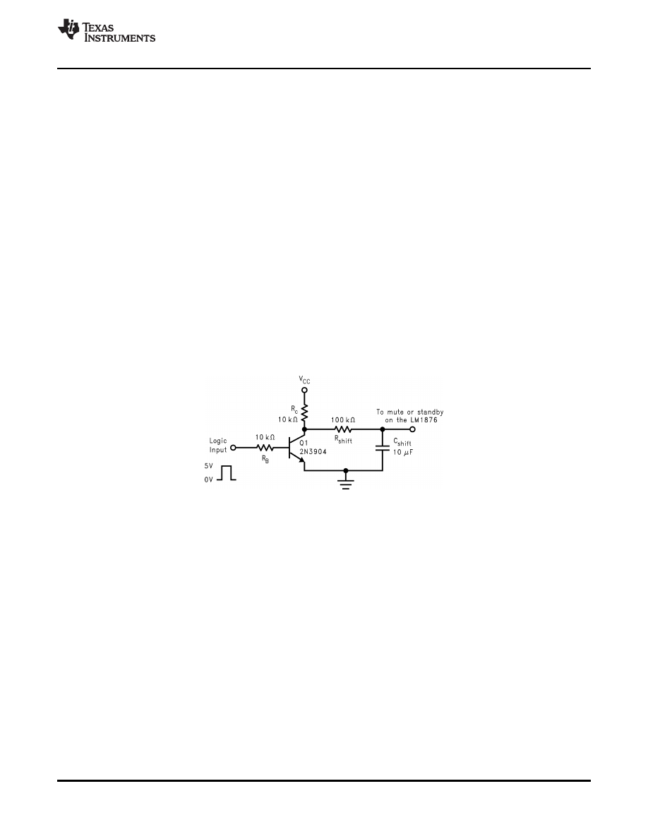
Figure 45. Level Shift Circuit
When the voltage at the Logic Input node is 0V, the 2N3904 is off and thus resistor R
c
pulls up mute or standby
input to the supply. This enables the mute or standby function. When the Logic Input is 5V, the 2N3904 is on
and consequently, the voltage at the collector is essentially 0V. This will disable the mute or standby function,
and thus the amplifier will be in its normal mode of operation. R
shift
, along with C
shift
, creates an RC time constant
that reduces transients when the mute or standby functions are enabled or disabled. Additionally, R
shift
limits the
current supplied by the internal logic gates of the LM1876 which insures device reliability. Refer to
and
in
for a more detailed description of these functions.
CLICKS AND POPS
In the typical application of the LM1876 as a split-supply audio power amplifier, the IC exhibits excellent click
and pop performance when utilizing the mute and standby modes. In addition, the device employs Under-
Voltage Protection, which eliminates unwanted power-up and power-down transients. The basis for these
functions are a stable and constant half-supply potential. In a split-supply application, ground is the stable half-
supply potential. But in a single-supply application, the half-supply needs to charge up just like the supply rail,
V
CC
. This makes the task of attaining a clickless and popless turn-on more challenging. Any uneven charging of
the amplifier inputs will result in output clicks and pops due to the differential input topology of the LM1876.
Copyright © 1999-2013, Texas Instruments Incorporated
19
Product Folder Links:
SNAS097C - MAY 1999 - REVISED APRIL 2013
To achieve a transient free power-up and power-down, the voltage seen at the input terminals should be ideally
the same. Such a signal will be common-mode in nature, and will be rejected by the LM1876. In
the
resistor R
INP
serves to keep the inputs at the same potential by limiting the voltage difference possible between
the two nodes. This should significantly reduce any type of turn-on pop, due to an uneven charging of the
amplifier inputs. This charging is based on a specific application loading and thus, the system designer may need
to adjust these values for optimal performance.
As shown in
the resistors labeled R
BI
help bias up the LM1876 off the half-supply node at the emitter of
the 2N3904. But due to the input and output coupling capacitors in the circuit, along with the negative feedback,
there are two different values of R
BI
, namely 10 k
Ω
and 200 k
Ω
. These resistors bring up the inputs at the same
rate resulting in a popless turn-on. Adjusting these resistors values slightly may reduce pops resulting from
power supplies that ramp extremely quick or exhibit overshoot during system turn-on.
AUDIO POWER AMPLlFIER DESIGN
Design a 15W/8
Ω
Audio Amplifier
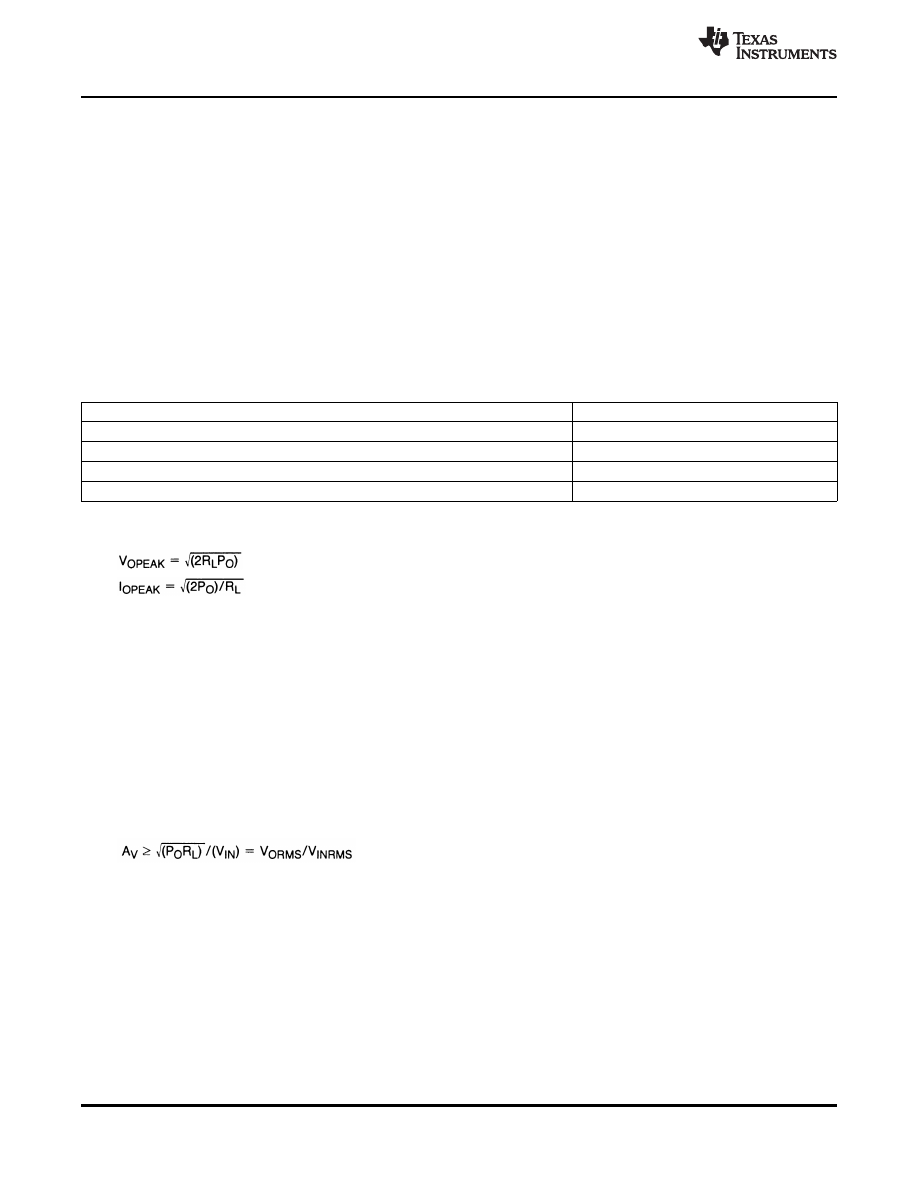
Given:
Power Output
15 Wrms
Load Impedance
8
Ω
Input Level
1 Vrms(max)
Input Impedance
47 k
Ω
Bandwidth
20 Hz
-
20 kHz ±0.25 dB
A designer must first determine the power supply requirements in terms of both voltage and current needed to
obtain the specified output power. V
OPEAK
can be determined from
and I
OPEAK
from
(4)
(5)
To determine the maximum supply voltage the following conditions must be considered. Add the dropout voltage
to the peak output swing V
OPEAK
, to get the supply rail at a current of I
OPEAK
. The regulation of the supply
determines the unloaded voltage which is usually about 15% higher. The supply voltage will also rise 10% during
high line conditions. Therefore the maximum supply voltage is obtained from the following equation.
Max supplies
± (V
OPEAK
+ V
OD
) (1 + regulation) (1.1)
(6)
For 15W of output power into an 8
Ω
load, the required V
OPEAK
is 15.49V. A minimum supply rail of 20.5V results
from adding V
OPEAK
and V
OD
. With regulation, the maximum supplies are ±26V and the required I
OPEAK
is 1.94A
from
It should be noted that for a dual 15W amplifier into an 8
Ω
load the I
OPEAK
drawn from the
supplies is twice 1.94 Apk or 3.88 Apk. At this point it is a good idea to check the Power Output vs Supply
Voltage to ensure that the required output power is obtainable from the device while maintaining low THD+N. In
addition, the designer should verify that with the required power supply voltage and load impedance, that the
required heatsink value
Θ
SA
is feasible given system cost and size constraints. Once the heatsink issues have
been addressed, the required gain can be determined from
.
(7)
From
the minimum A
V
is:
A
V
≥
11.
By selecting a gain of 21, and with a feedback resistor, R
f
= 20 k
Ω
, the value of R
i
follows from
R
i
= R
f
(A
V
-
1)
(8)
Thus with R
i
= 1 k
Ω
a non-inverting gain of 21 will result. Since the desired input impedance was 47 k
Ω
, a value
of 47 k
Ω
was selected for R
IN
. The final design step is to address the bandwidth requirements which must be
stated as a pair of
-
3 dB frequency points. Five times away from a
-
3 dB point is 0.17 dB down from passband
response which is better than the required ±0.25 dB specified. This fact results in a low and high frequency pole
of 4 Hz and 100 kHz respectively. As stated in
, R
i
in conjunction with C
i
create
a high-pass filter.
C
i
≥
1/(2
Ï
* 1 k
Ω
* 4 Hz) = 39.8
μ
F;
use 39
μ
F.
(9)
20
Copyright © 1999-2013, Texas Instruments Incorporated
Product Folder Links:

SNAS097C - MAY 1999 - REVISED APRIL 2013
The high frequency pole is determined by the product of the desired high frequency pole, f
H
, and the gain, A
V
.
With a A
V
= 21 and f
H
= 100 kHz, the resulting GBWP is 2.1 MHz, which is less than the minimum GBWP of the
LM1876 of 5 MHz. This will ensure that the high frequency response of the amplifier will be no worse than 0.17
dB down at 20 kHz which is well within the bandwidth requirements of the design.
Copyright © 1999-2013, Texas Instruments Incorporated
21
Product Folder Links:

SNAS097C - MAY 1999 - REVISED APRIL 2013
REVISION HISTORY
Changes from Revision B (April 2013) to Revision C
Page
Changed layout of National Data Sheet to TI format ..........................................................................................................
22
Copyright © 1999-2013, Texas Instruments Incorporated
Product Folder Links:
PACKAGE OPTION ADDENDUM
www.ti.com
6-May-2016
Addendum-Page 1
PACKAGING INFORMATION
Orderable Device
Status
(1)
Package Type Package
Drawing
Pins Package
Qty
Eco Plan
(2)
Lead/Ball Finish
(6)
MSL Peak Temp
(3)
Op Temp ( °C)
Device Marking
(4/5)
Samples
LM1876T
LIFEBUY
TO-220
NDL
15
20
TBD
Call TI
Call TI
-20 to 85
LM1876T
LM1876T/NOPB
LIFEBUY
TO-220
NDL
15
20
Green (RoHS
& no Sb/Br)
CU SN
Level-1-NA-UNLIM
-20 to 85
LM1876T
LM1876TF
LIFEBUY
TO-220
NDB
15
20
TBD
Call TI
Call TI
-20 to 85
LM1876TF
LM1876TF/NOPB
NRND
TO-220
NDB
15
20
Pb-Free (RoHS
Exempt)
CU SN
Level-1-NA-UNLIM
-20 to 85
LM1876TF
(1)
The marketing status values are defined as follows:
ACTIVE: Product device recommended for new designs.
LIFEBUY: TI has announced that the device will be discontinued, and a lifetime-buy period is in effect.
NRND: Not recommended for new designs. Device is in production to support existing customers, but TI does not recommend using this part in a new design.
PREVIEW: Device has been announced but is not in production. Samples may or may not be available.
OBSOLETE: TI has discontinued the production of the device.
(2)
Eco Plan - The planned eco-friendly classification: Pb-Free (RoHS), Pb-Free (RoHS Exempt), or Green (RoHS & no Sb/Br) - please check
for the latest availability
information and additional product content details.
TBD: The Pb-Free/Green conversion plan has not been defined.
Pb-Free (RoHS): TI's terms "Lead-Free" or "Pb-Free" mean semiconductor products that are compatible with the current RoHS requirements for all 6 substances, including the requirement that
lead not exceed 0.1% by weight in homogeneous materials. Where designed to be soldered at high temperatures, TI Pb-Free products are suitable for use in specified lead-free processes.
Pb-Free (RoHS Exempt): This component has a RoHS exemption for either 1) lead-based flip-chip solder bumps used between the die and package, or 2) lead-based die adhesive used between
the die and leadframe. The component is otherwise considered Pb-Free (RoHS compatible) as defined above.
Green (RoHS & no Sb/Br): TI defines "Green" to mean Pb-Free (RoHS compatible), and free of Bromine (Br) and Antimony (Sb) based flame retardants (Br or Sb do not exceed 0.1% by weight
in homogeneous material)
(3)
MSL, Peak Temp. - The Moisture Sensitivity Level rating according to the JEDEC industry standard classifications, and peak solder temperature.
(4)
There may be additional marking, which relates to the logo, the lot trace code information, or the environmental category on the device.
(5)
Multiple Device Markings will be inside parentheses. Only one Device Marking contained in parentheses and separated by a "~" will appear on a device. If a line is indented then it is a continuation
of the previous line and the two combined represent the entire Device Marking for that device.
(6)
Lead/Ball Finish - Orderable Devices may have multiple material finish options. Finish options are separated by a vertical ruled line. Lead/Ball Finish values may wrap to two lines if the finish
value exceeds the maximum column width.
Important Information and Disclaimer:The information provided on this page represents TI's knowledge and belief as of the date that it is provided. TI bases its knowledge and belief on information
provided by third parties, and makes no representation or warranty as to the accuracy of such information. Efforts are underway to better integrate information from third parties. TI has taken and
PACKAGE OPTION ADDENDUM
www.ti.com
6-May-2016
Addendum-Page 2
continues to take reasonable steps to provide representative and accurate information but may not have conducted destructive testing or chemical analysis on incoming materials and chemicals.
TI and TI suppliers consider certain information to be proprietary, and thus CAS numbers and other limited information may not be available for release.
In no event shall TI's liability arising out of such information exceed the total purchase price of the TI part(s) at issue in this document sold by TI to Customer on an annual basis.
MECHANICAL DATA
NDL0015A
www.ti.com
TA15A (Rev B)
MECHANICAL DATA
NDB0015B
www.ti.com
TF15B (REV B)

IMPORTANT NOTICE
Texas Instruments Incorporated and its subsidiaries (TI) reserve the right to make corrections, enhancements, improvements and other
changes to its semiconductor products and services per JESD46, latest issue, and to discontinue any product or service per JESD48, latest
issue. Buyers should obtain the latest relevant information before placing orders and should verify that such information is current and
complete. All semiconductor products (also referred to herein as components) are sold subject to TIs terms and conditions of sale
supplied at the time of order acknowledgment.
TI warrants performance of its components to the specifications applicable at the time of sale, in accordance with the warranty in TIs terms
and conditions of sale of semiconductor products. Testing and other quality control techniques are used to the extent TI deems necessary
to support this warranty. Except where mandated by applicable law, testing of all parameters of each component is not necessarily
performed.
TI assumes no liability for applications assistance or the design of Buyers products. Buyers are responsible for their products and
applications using TI components. To minimize the risks associated with Buyers products and applications, Buyers should provide
adequate design and operating safeguards.
TI does not warrant or represent that any license, either express or implied, is granted under any patent right, copyright, mask work right, or
other intellectual property right relating to any combination, machine, or process in which TI components or services are used. Information
published by TI regarding third-party products or services does not constitute a license to use such products or services or a warranty or
endorsement thereof. Use of such information may require a license from a third party under the patents or other intellectual property of the
third party, or a license from TI under the patents or other intellectual property of TI.
Reproduction of significant portions of TI information in TI data books or data sheets is permissible only if reproduction is without alteration
and is accompanied by all associated warranties, conditions, limitations, and notices. TI is not responsible or liable for such altered
documentation. Information of third parties may be subject to additional restrictions.
Resale of TI components or services with statements different from or beyond the parameters stated by TI for that component or service
voids all express and any implied warranties for the associated TI component or service and is an unfair and deceptive business practice.
TI is not responsible or liable for any such statements.
Buyer acknowledges and agrees that it is solely responsible for compliance with all legal, regulatory and safety-related requirements
concerning its products, and any use of TI components in its applications, notwithstanding any applications-related information or support
that may be provided by TI. Buyer represents and agrees that it has all the necessary expertise to create and implement safeguards which
anticipate dangerous consequences of failures, monitor failures and their consequences, lessen the likelihood of failures that might cause
harm and take appropriate remedial actions. Buyer will fully indemnify TI and its representatives against any damages arising out of the use
of any TI components in safety-critical applications.
In some cases, TI components may be promoted specifically to facilitate safety-related applications. With such components, TIs goal is to
help enable customers to design and create their own end-product solutions that meet applicable functional safety standards and
requirements. Nonetheless, such components are subject to these terms.
No TI components are authorized for use in FDA Class III (or similar life-critical medical equipment) unless authorized officers of the parties
have executed a special agreement specifically governing such use.
Only those TI components which TI has specifically designated as military grade or enhanced plastic are designed and intended for use in
military/aerospace applications or environments. Buyer acknowledges and agrees that any military or aerospace use of TI components
which have not been so designated is solely at the Buyer's risk, and that Buyer is solely responsible for compliance with all legal and
regulatory requirements in connection with such use.
TI has specifically designated certain components as meeting ISO/TS16949 requirements, mainly for automotive use. In any case of use of
non-designated products, TI will not be responsible for any failure to meet ISO/TS16949.
Products
Applications
Audio
Automotive and Transportation
Amplifiers
Communications and Telecom
Data Converters
Computers and Peripherals
DLP ® Products
Consumer Electronics
DSP
Energy and Lighting
Clocks and Timers
Industrial
Interface
Medical
Logic
Security
Power Mgmt
Space, Avionics and Defense
Microcontrollers
Video and Imaging
RFID
OMAP Applications Processors
TI E2E Community
Wireless Connectivity
Mailing Address: Texas Instruments, Post Office Box 655303, Dallas, Texas 75265
Copyright © 2016, Texas Instruments Incorporated
Document Outline

