| Secciones |
|---|
| Foros Electrónica |
|
|
| Boletines de correo |
 |
, ,
SNOSBT3I - JANUARY 2000 - REVISED DECEMBER 2014
LMx58-N Low-Power, Dual-Operational Amplifiers
1 Features
3 Description
The LM158 series consists of two independent, high
1
Available in 8-Bump DSBGA Chip-Sized Package,
gain, internally frequency compensated operational
(See AN-1112,
)
amplifiers which were designed specifically to operate
Internally Frequency Compensated for Unity Gain
from a single power supply over a wide range of
Large DC Voltage Gain:
100 dB
voltages. Operation from split power supplies is also
possible and the low power supply current drain is
Wide Bandwidth (Unity Gain):
1 MHz
independent of the magnitude of the power supply
(Temperature Compensated)
voltage.
Wide Power Supply Range:
Application areas include transducer amplifiers, dc
-
Single Supply:
3V to 32V
gain blocks and all the conventional op-amp circuits
-
Or Dual Supplies:
±1.5V to ±16V
which now can be more easily implemented in single
Very Low Supply Current Drain (500
power supply systems. For example, the LM158
series can be directly operated off of the standard
μA)Essentially Independent of Supply Voltage
3.3-V power supply voltage which is used in digital
Low Input Offset Voltage:
2 mV
systems and will easily provide the required interface
Input Common-Mode Voltage Range Includes
electronics without requiring the additional ±15V
Ground
power supplies.
Differential Input Voltage Range Equal to the
The LM358 and LM2904 are available in a chip sized
Power Supply Voltage
package
(8-Bump
DSBGA)
using
TI's
DSBGA
Large Output Voltage Swing
package technology.
Unique Characteristics:
Device
-
In the Linear Mode the Input Common-Mode
PART NUMBER
PACKAGE
BODY SIZE (NOM)
Voltage Range Includes Ground and the
TO-CAN (8)
9.08 mm x 9.09 mm
Output Voltage Can Also Swing to Ground,
LM158-N
CDIP (8)
10.16 mm x 6.502 mm
even though Operated from Only a Single
LM258-N
TO-CAN (8)
9.08 mm x 9.09 mm
Power Supply Voltage.
DSBGA (8)
1.31 mm x 1.31 mm
-
The Unity Gain Cross Frequency is
LM2904-N
SOIC (8)
4.90 mm x 3.91 mm
Temperature Compensated.
PDIP (8)
9.81 mm x 6.35 mm
-
The Input Bias Current is also Temperature
TO-CAN (8)
9.08 mm x 9.09 mm
Compensated.
DSBGA (8)
1.31 mm x 1.31 mm
Advantages:
LM358-N
SOIC (8)
4.90 mm x 3.91 mm
-
Two Internally Compensated Op Amps
PDIP (8)
9.81 mm x 6.35 mm
-
Eliminates Need for Dual Supplies
(1) For all available packages, see the orderable addendum at
-
Allows Direct Sensing Near GND and V
OUT
the end of the datasheet.
Also Goes to GND
-
Compatible with All Forms of Logic
Voltage Controlled Oscillator (VCO)
-
Power Drain Suitable for Battery Operation
2 Applications
Active Filters
General Signal Conditioning and Amplification
4- to 20-mA Current Loop Transmitters
1
An IMPORTANT NOTICE at the end of this data sheet addresses availability, warranty, changes, use in safety-critical applications,
intellectual property matters and other important disclaimers. PRODUCTION DATA.

, , ,
SNOSBT3I - JANUARY 2000 - REVISED DECEMBER 2014
Table of Contents
7.3
Feature Description.................................................
1
Features ..................................................................
7.4
Device Functional Modes........................................
2
Applications ...........................................................
8
Application and Implementation ........................
3
Description .............................................................
8.1
Application Information............................................
4
Revision History.....................................................
8.2
Typical Applications ................................................
5
Pin Configuration and Functions .........................
9
Power Supply Recommendations ......................
6
Specifications.........................................................
10
Layout...................................................................
6.1
Absolute Maximum Ratings ......................................
10.1
Layout Guidelines .................................................
6.2
ESD Ratings ............................................................
10.2
Layout Example ....................................................
6.3
Recommended Operating Conditions .......................
11
Device and Documentation Support .................
6.4
Thermal Information ..................................................
11.1
Related Links ........................................................
6.5
Electrical Characteristics: LM158A, LM358A, LM158,
LM258 ........................................................................
11.2
Trademarks ...........................................................
6.6
Electrical Characteristics: LM358, LM2904...............
11.3
Electrostatic Discharge Caution ............................
6.7
Typical Characteristics ..............................................
11.4
Glossary ................................................................
7
Detailed Description ............................................
12
Mechanical, Packaging, and Orderable
Information ...........................................................
7.1
Overview .................................................................
7.2
Functional Block Diagram .......................................
4 Revision History
NOTE: Page numbers for previous revisions may differ from page numbers in the current version.
Changes from Revision H (March 2013) to Revision I
Page
Added Pin Configuration and Functions section, ESD Ratings table, Feature Description section, Device Functional
Modes, Application and Implementation section, Power Supply Recommendations section, Layout section, Device
and Documentation Support section, and Mechanical, Packaging, and Orderable Information section ..............................
Changes from Revision G (March 2013) to Revision H
Page
Changed layout of National Data Sheet to TI format ...........................................................................................................
2
Copyright © 2000-2014, Texas Instruments Incorporated
Product Folder Links:
, ,
SNOSBT3I - JANUARY 2000 - REVISED DECEMBER 2014
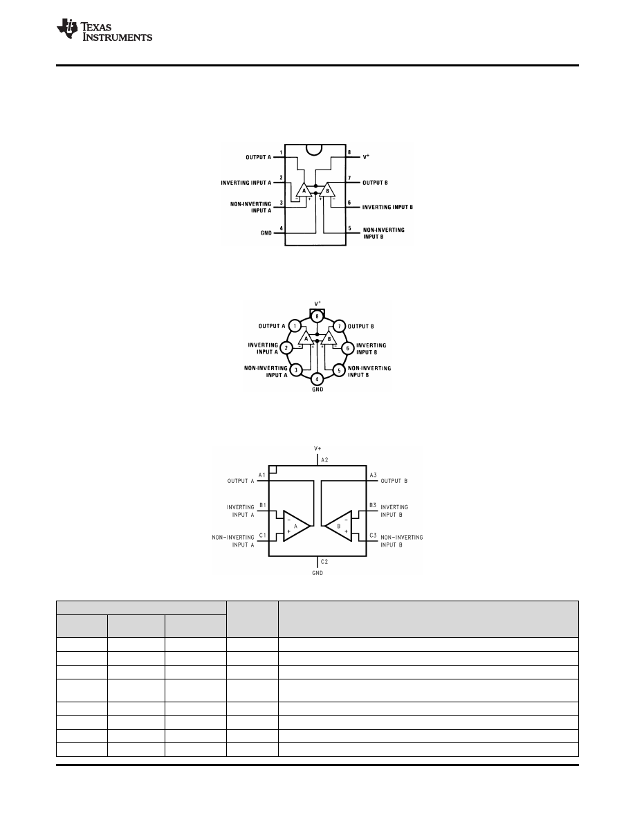
5 Pin Configuration and Functions
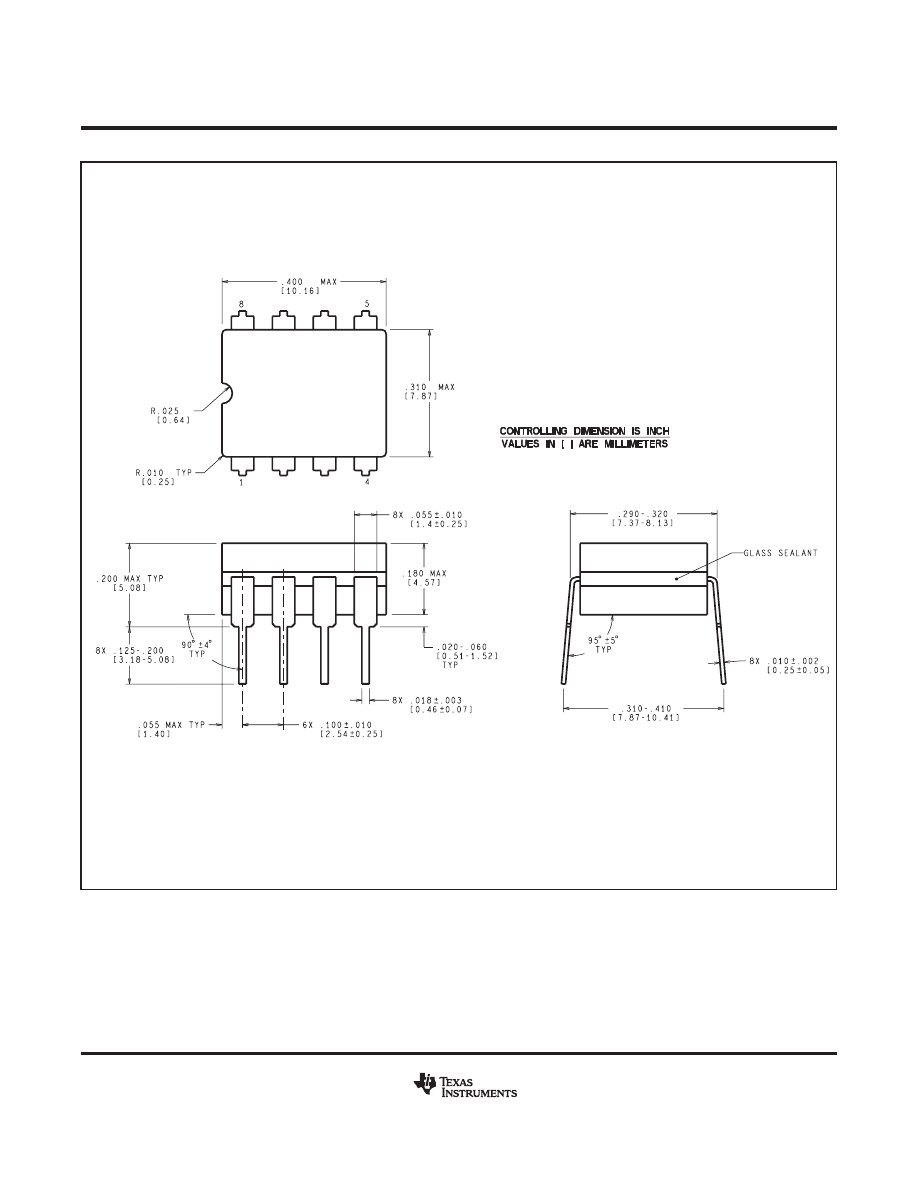
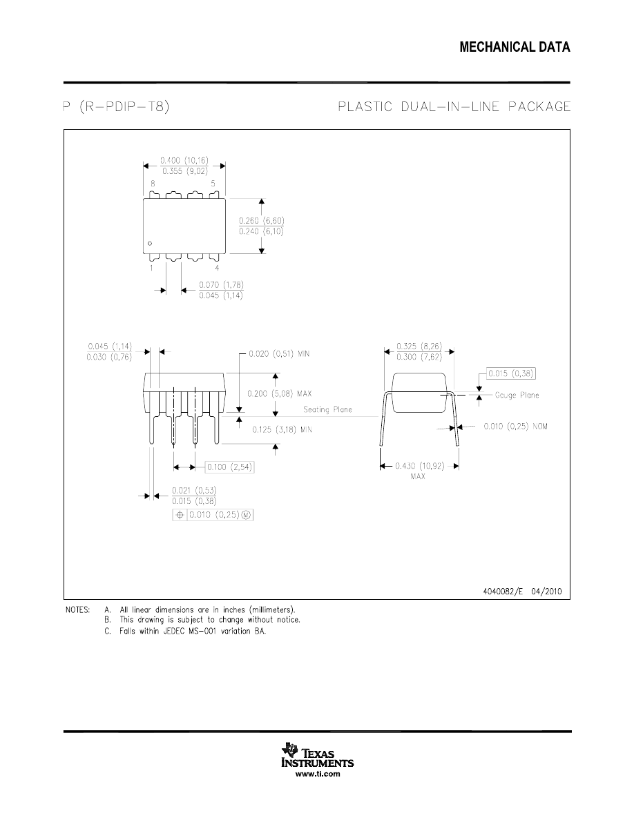
D, P, and NAB Package
8-Pin SOIC, PDIP, and CDIP
Top View
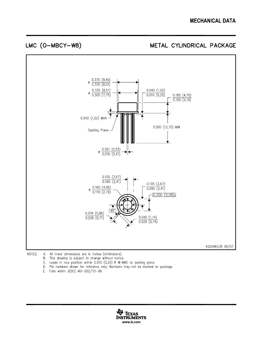
LMC Package
8-Pin TO-99
Top View
YPB Package
8-Pin DSBGA
Top View
Pin Functions
PIN
TYPE
DESCRIPTION
D/P/LMC
DSBGA NO.
NAME
NO.
1
A1
OUTA
O
Output , Channel A
2
B1
-INA
I
Inverting Input, Channel A
3
C1
+INA
I
Non-Inverting Input, Channel A
Ground for Single supply configurations. negative supply for dual supply
4
C2
GND / V-
P
configurations
5
C3
+INB
I
Output, Channel B
6
B3
-INB
I
Inverting Input, Channel B
7
A3
OUTB
O
Non-Inverting Input, Channel B
8
A2
V+
P
Positive Supply
Copyright © 2000-2014, Texas Instruments Incorporated
3
Product Folder Links:
, , ,
SNOSBT3I - JANUARY 2000 - REVISED DECEMBER 2014
6 Specifications
6.1 Absolute Maximum Ratings
See
(1) (2) (3)
.
LM158, LM258,
LM358, LM158A,
LM2904
UNIT
LM258A, LM358A
MIN
MAX
MIN
MAX
Supply Voltage, V
+
32
26
V
Differential Input Voltage
32
26
V
Input Voltage
-0.3
32
-0.3
26
V
Power Dissipation
(4)
PDIP (P)
830
830
mW
TO-99 (LMC)
550
mW
SOIC (D)
530
530
mW
DSBGA (YPB)
435
mW
Output Short-Circuit to V
+
≤ 15 V and T
A
= 25 °C
Continuous
Continuou
GND
(One
s
Amplifier)
(5)
Input Current (V
IN
<
-0.3V)
(6)
50
50
mA
Temperature
-55
125
°C
PDIP Package (P): Soldering (10 seconds)
260
260
°C
SOIC Package (D)
Vapor Phase (60
215
215
°C
seconds)
Infrared (15 seconds)
220
220
°C
Lead Temperature
PDIP (P): (Soldering, 10 seconds)
260
260
°C
TO-99 (LMC): (Soldering, 10 seconds)
300
300
°C
Storage temperature, T
stg
-65
150
-65
150
°C
(1)
Absolute Maximum Ratings indicate limits beyond which damage to the device may occur. Recommended Operating Conditions indicate
conditions for which the device is intended to be functional, but specific performance is not ensured. For ensured specifications and the
test conditions, see the Electrical Characteristics.
(2)
Refer to RETS158AX for LM158A military specifications and to RETS158X for LM158 military specifications.
(3)
If Military/Aerospace specified devices are required, please contact the TI Sales Office/Distributors for availability and specifications.
(4)
For operating at high temperatures, the LM358/LM358A, LM2904 must be derated based on a 125 °C maximum junction temperature
and a thermal resistance of 120 °C/W for PDIP, 182 °C/W for TO-99, 189 °C/W for SOIC package, and 230 °C/W for DSBGA, which
applies for the device soldered in a printed circuit board, operating in a still air ambient. The LM258/LM258A and LM158/LM158A can be
derated based on a +150 °C maximum junction temperature. The dissipation is the total of both amplifiersuse external resistors, where
possible, to allow the amplifier to saturate or to reduce the power which is dissipated in the integrated circuit.
(5)
Short circuits from the output to V
+
can cause excessive heating and eventual destruction. When considering short circuits to ground,
the maximum output current is approximately 40 mA independent of the magnitude of V
+
. At values of supply voltage in excess of +15
V, continuous short-circuits can exceed the power dissipation ratings and cause eventual destruction. Destructive dissipation can result
from simultaneous shorts on all amplifiers.
(6)
This input current will only exist when the voltage at any of the input leads is driven negative. It is due to the collector-base junction of
the input PNP transistors becoming forward biased and thereby acting as input diode clamps. In addition to this diode action, there is
also lateral NPN parasitic transistor action on the IC chip. This transistor action can cause the output voltages of the op amps to go to
the V
+
voltage level (or to ground for a large overdrive) for the time duration that an input is driven negative. This is not destructive and
normal output states will re-establish when the input voltage, which was negative, again returns to a value greater than
-0.3 V (at 25 °C).
6.2 ESD Ratings
VALUE
UNIT
V
(ESD)
Electrostatic discharge
Human-body model (HBM), per ANSI/ESDA/JEDEC JS-001
(1)
±250
V
(1)
JEDEC document JEP155 states that 500-V HBM allows safe manufacturing with a standard ESD control process.
4
Copyright © 2000-2014, Texas Instruments Incorporated
Product Folder Links:
, ,
SNOSBT3I - JANUARY 2000 - REVISED DECEMBER 2014
6.3 Recommended Operating Conditions
over operating free-air temperature range (unless otherwise noted)
MIN
MAX
UNIT
Supply Voltage (V+ - V-):LM158. LM258, LM358
3 ( ±1.5)
32 ( ±16)
V
Supply Voltage (V+ - V-):LM2904
3 ( ±1.5)
26 ( ±13)
V
Operating Temperature: LM158
-55
125
°C
Operating Temperature: LM258
-25
85
°C
Operating Temperature: LM358
0
70
°C
Operating Temperature: LM2904
-40
85
°C
6.4 Thermal Information
LM158-N,
LM158-N
LM2904-N, LM358-N
LM258-N,
LM358-N
THERMAL METRIC
(1)
UNIT
LMC
NAB
YPB
D
P
8 PINS
R
ΘJA
Junction-to-ambient thermal resistance
155
132
230
189
120
°C/W
(1)
For more information about traditional and new thermal metrics, see the IC Package Thermal Metrics application report,
6.5 Electrical Characteristics: LM158A, LM358A, LM158, LM258
V
+
= +5.0 V, See
(1)
, unless otherwise stated
LM158A
LM358A
LM158, LM258
PARAMETER
TEST CONDITIONS
UNIT
MIN
TYP
MAX
MIN
TYP
MAX
MIN
TYP
MAX
Input Offset Voltage
See
(2)
, T
A
= 25 °C
1
2
2
3
2
5
mV
Input Bias Current
I
IN(+)
or I
IN(
-)
, T
A
= 25 °C,
20
50
45
100
45
150
nA
V
CM
= 0 V,
(3)
Input Offset Current
I
IN(+)
- I
IN(
-)
, V
CM
= 0V, T
A
=
2
10
5
30
3
30
nA
25 °C
Input Common-Mode
V
+
= 30 V,
(4)
V
+
-1.
0
0
V
+
-1.5
0
V
+
-1.5
V
Voltage Range
(LM2904, V
+
= 26V), T
A
=
5
25 °C
Supply Current
Over Full Temperature
Range
R
L
=
on All Op Amps
V
+
= 30V (LM2904 V
+
= 26V)
1
2
1
2
1
2
mA
V
+
= 5V
0.5
1.2
0.5
1.2
0.5
1.2
mA
Large Signal Voltage Gain
V
+
= 15 V, T
A
= 25 °C,
R
L
≥ 2 kΩ, (For V
O
= 1 V to
50
100
25
100
50
100
V/mV
11 V)
Common-Mode
T
A
= 25 °C,
70
85
65
85
70
85
dB
Rejection Ratio
V
CM
= 0 V to V
+
-1.5 V
Power Supply
V
+
= 5 V to 30 V
65
100
65
100
65
100
dB
Rejection Ratio
(LM2904, V
+
= 5 V to 26 V),
T
A
= 25 °C
(1)
These specifications are limited to -55 °C
≤ T
A
≤ +125 °C for the LM158/LM158A. With the LM258/LM258A, all temperature specifications
are limited to
-25 °C ≤ T
A
≤ 85 °C, the LM358/LM358A temperature specifications are limited to 0 °C ≤ T
A
≤ 70 °C, and the LM2904
specifications are limited to -40 °C
≤ T
A
≤ 85 °C.
(2)
V
O
1.4 V, R
S
= 0
Ω with V
+
from 5 V to 30 V; and over the full input common-mode range (0 V to V
+
-1.5 V) at 25 °C. For LM2904, V
+
from 5 V to 26 V.
(3)
The direction of the input current is out of the IC due to the PNP input stage. This current is essentially constant, independent of the
state of the output so no loading change exists on the input lines.
(4)
The input common-mode voltage of either input signal voltage should not be allowed to go negative by more than 0.3 V (at 25 °C). The
upper end of the common-mode voltage range is V
+
-1.5 V (at 25 °C), but either or both inputs can go to 32 V without damage (26 V for
LM2904), independent of the magnitude of V
+
.
Copyright © 2000-2014, Texas Instruments Incorporated
5
Product Folder Links:
, , ,
SNOSBT3I - JANUARY 2000 - REVISED DECEMBER 2014
Electrical Characteristics: LM158A, LM358A, LM158, LM258 (continued)
V
+
= +5.0 V, See
unless otherwise stated
LM158A
LM358A
LM158, LM258
PARAMETER
TEST CONDITIONS
UNIT
MIN
TYP
MAX
MIN
TYP
MAX
MIN
TYP
MAX
Power Supply
V
+
= 5 V to 30 V
65
100
65
100
65
100
dB
Rejection Ratio
(LM2904, V
+
= 5 V to 26 V),
T
A
= 25 °C
Amplifier-to-Amplifier
f = 1 kHz to 20 kHz, T
A
=
-120
-120
-120
dB
Coupling
25 °C (Input Referred), See
(5)
Output Current
Source
V
IN
+
= 1 V,
V
IN
-
= 0 V,
20
40
20
40
20
40
mA
V
+
= 15 V,
V
O
= 2 V, T
A
= 25 °C
Sink
V
IN
-
= 1 V, V
IN
+
= 0 V
V
+
= 15 V, T
A
= 25 °C,
10
20
10
20
10
20
mA
V
O
= 2 V
V
IN
-
= 1 V,
V
IN
+
= 0 V
12
50
12
50
12
50
μA
T
A
= 25 °C, V
O
= 200 mV,
V
+
= 15 V
Short Circuit to Ground
T
A
= 25 °C, See
(6)
, V
+
= 15 V
40
60
40
60
40
60
mA
Input Offset Voltage
See
(2)
4
5
7
mV
Input Offset Voltage Drift
R
S
= 0
Ω
7
15
7
20
7
μV/ °C
Input Offset Current
I
IN(+)
- I
IN(
-)
30
75
100
nA
Input Offset Current Drift
R
S
= 0
Ω
10
200
10
300
10
pA/ °C
Input Bias Current
I
IN(+)
or I
IN(
-)
40
100
40
200
40
300
nA
Input Common-Mode
V
+
= 30 V, See
(4)
(LM2904,
0
V
+
-2
0
V
+
-2
0
V
+
-2
V
Voltage Range
V
+
= 26 V)
Large Signal Voltage Gain
V
+
= +15 V
(V
O
= 1 V to 11 V)
25
15
25
V/mV
R
L
≥ 2 kΩ
Output
V
OH
V
+
= +30 V
R
L
= 2
26
26
26
V
k
Ω
Voltage
R
L
=
27
28
27
28
27
28
V
(LM2904, V
+
= 26 V)
10 k
Ω
Swing
V
OL
V
+
= 5V, R
L
= 10 k
Ω
5
20
5
20
5
20
mV
Output Current
Source
V
IN
+
= +1 V, V
IN
-
= 0 V,
10
20
10
20
10
20
mA
V
+
= 15 V, V
O
= 2 V
Sink
V
IN
-
= +1 V, V
IN
+
= 0 V,
10
15
5
8
5
8
mA
V
+
= 15 V, V
O
= 2 V
(5)
Due to proximity of external components, insure that coupling is not originating via stray capacitance between these external parts. This
typically can be detected as this type of capacitance increases at higher frequencies.
(6)
Short circuits from the output to V
+
can cause excessive heating and eventual destruction. When considering short circuits to ground,
the maximum output current is approximately 40 mA independent of the magnitude of V
+
. At values of supply voltage in excess of +15
V, continuous short-circuits can exceed the power dissipation ratings and cause eventual destruction. Destructive dissipation can result
from simultaneous shorts on all amplifiers.
6
Copyright © 2000-2014, Texas Instruments Incorporated
Product Folder Links:
, ,
SNOSBT3I - JANUARY 2000 - REVISED DECEMBER 2014
6.6 Electrical Characteristics: LM358, LM2904
V
+
= +5.0 V, See
(1)
, unless otherwise stated
LM358
LM2904
PARAMETER
TEST CONDITIONS
UNIT
MIN
TYP
MAX
MIN
TYP
MAX
Input Offset Voltage
See
(2)
, T
A
= 25 °C
2
7
2
7
mV
Input Bias Current
I
IN(+)
or I
IN(
-)
, T
A
= 25 °C,
45
250
45
250
nA
V
CM
= 0 V, See
(3)
Input Offset Current
I
IN(+)
- I
IN(
-)
, V
CM
= 0 V, T
A
= 25 °C
5
50
5
50
nA
Input Common-Mode
V
+
= 30 V, See
(4)
V
+
-1.
0
0
V
+
-1.5
V
Voltage Range
(LM2904, V
+
= 26 V), T
A
= 25 °C
5
Supply Current
Over Full Temperature Range
R
L
=
on All Op Amps
V
+
= 30 V (LM2904 V
+
= 26 V)
1
2
1
2
mA
V
+
= 5 V
0.5
1.2
0.5
1.2
mA
Large Signal Voltage
V
+
= 15V, T
A
= 25 °C,
Gain
R
L
≥ 2 kΩ, (For V
O
= 1 V to 11 V)
25
100
25
100
V/mV
Common-Mode
T
A
= 25 °C,
65
85
50
70
dB
Rejection Ratio
V
CM
= 0 V to V
+
-1.5 V
Power Supply
V
+
= 5 V to 30 V
65
100
50
100
dB
Rejection Ratio
(LM2904, V
+
= 5 V to 26 V), T
A
= 25 °C
Amplifier-to-Amplifier Coupling
f = 1 kHz to 20 kHz, T
A
= 25 °C
-120
-120
dB
(Input Referred), See
(5)
Output Current
Source
V
IN
+
= 1 V,
V
IN
-
= 0 V,
20
40
20
40
mA
V
+
= 15 V,
V
O
= 2 V, T
A
= 25 °C
Sink
V
IN
-
= 1 V, V
IN
+
= 0 V
V
+
= 15V, T
A
= 25 °C,
10
20
10
20
mA
V
O
= 2 V
V
IN
-
= 1 V,
V
IN
+
= 0 V
12
50
12
50
μA
T
A
= 25 °C, V
O
= 200 mV,
V
+
= 15 V
Short Circuit to Ground
T
A
= 25 °C, See
(6)
, V
+
= 15 V
40
60
40
60
mA
Input Offset Voltage
See
(2)
9
10
mV
Input Offset Voltage Drift
R
S
= 0
Ω
7
7
μV/ °C
Input Offset Current
I
IN(+)
- I
IN(
-)
150
45
200
nA
Input Offset Current Drift
R
S
= 0
Ω
10
10
pA/ °C
Input Bias Current
I
IN(+)
or I
IN(
-)
40
500
40
500
nA
(1)
These specifications are limited to -55 °C
≤ T
A
≤ +125 °C for the LM158/LM158A. With the LM258/LM258A, all temperature specifications
are limited to
-25 °C ≤ T
A
≤ 85 °C, the LM358/LM358A temperature specifications are limited to 0 °C ≤ T
A
≤ 70 °C, and the LM2904
specifications are limited to -40 °C
≤ T
A
≤ 85 °C.
(2)
V
O
1.4 V, R
S
= 0
Ω with V
+
from 5 V to 30 V; and over the full input common-mode range (0 V to V
+
-1.5 V) at 25 °C. For LM2904, V
+
from 5 V to 26 V.
(3)
The direction of the input current is out of the IC due to the PNP input stage. This current is essentially constant, independent of the
state of the output so no loading change exists on the input lines.
(4)
The input common-mode voltage of either input signal voltage should not be allowed to go negative by more than 0.3 V (at 25 °C). The
upper end of the common-mode voltage range is V
+
-1.5 V (at 25 °C), but either or both inputs can go to 32 V without damage (26 V for
LM2904), independent of the magnitude of V
+
.
(5)
Due to proximity of external components, insure that coupling is not originating via stray capacitance between these external parts. This
typically can be detected as this type of capacitance increases at higher frequencies.
(6)
Short circuits from the output to V
+
can cause excessive heating and eventual destruction. When considering short circuits to ground,
the maximum output current is approximately 40 mA independent of the magnitude of V
+
. At values of supply voltage in excess of +15
V, continuous short-circuits can exceed the power dissipation ratings and cause eventual destruction. Destructive dissipation can result
from simultaneous shorts on all amplifiers.
Copyright © 2000-2014, Texas Instruments Incorporated
7
Product Folder Links:
, , ,
SNOSBT3I - JANUARY 2000 - REVISED DECEMBER 2014
Electrical Characteristics: LM358, LM2904 (continued)
V
+
= +5.0 V, See
unless otherwise stated
LM358
LM2904
PARAMETER
TEST CONDITIONS
UNIT
MIN
TYP
MAX
MIN
TYP
MAX
Input Common-Mode
V
+
= 30 V, See
(4)
(LM2904, V
+
= 26 V)
0
V
+
-2
0
V
+
-2
V
Voltage Range
Large Signal Voltage Gain
V
+
= +15 V
(V
O
= 1 V to 11 V)
15
15
V/mV
R
L
≥ 2 kΩ
Output
V
OH
V
+
= 30 V
R
L
= 2 k
Ω
26
22
V
Voltage
(LM2904, V
+
= 26 V)
R
L
= 10 k
Ω
27
28
23
24
V
Swing
V
OL
V
+
= 5 V, R
L
= 10 k
Ω
5
20
5
100
mV
Output Current
Source
V
IN
+
= 1 V, V
IN
-
= 0 V,
10
20
10
20
mA
V
+
= 15 V, V
O
= 2 V
Sink
V
IN
-
= 1 V, V
IN
+
= 0 V,
5
8
5
8
mA
V
+
= 15 V, V
O
= 2 V
8
Copyright © 2000-2014, Texas Instruments Incorporated
Product Folder Links:
, ,
SNOSBT3I - JANUARY 2000 - REVISED DECEMBER 2014
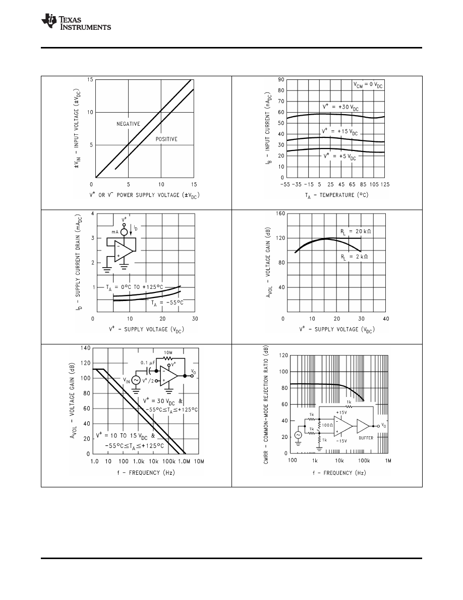
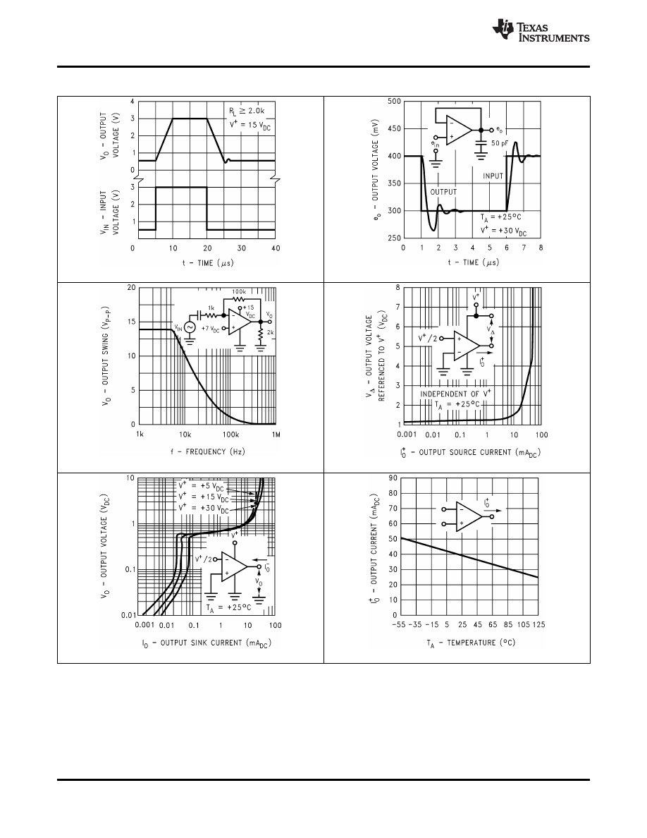
6.7 Typical Characteristics
Figure 1. Input Voltage Range
Figure 2. Input Current
Figure 3. Supply Current
Figure 4. Voltage Gain
Figure 6. Common-Mode Rejection Ratio
Figure 5. Open Loop Frequency Response
Copyright © 2000-2014, Texas Instruments Incorporated
9
Product Folder Links:
, , ,
SNOSBT3I - JANUARY 2000 - REVISED DECEMBER 2014
Typical Characteristics (continued)
Figure 8. Voltage Follower Pulse Response (Small Signal)
Figure 7. Voltage Follower Pulse Response
Figure 9. Large Signal Frequency Response
Figure 10. Output Characteristics Current Sourcing
Figure 11. Output Characteristics Current Sinking
Figure 12. Current Limiting
10
Copyright © 2000-2014, Texas Instruments Incorporated
Product Folder Links:
, ,
SNOSBT3I - JANUARY 2000 - REVISED DECEMBER 2014
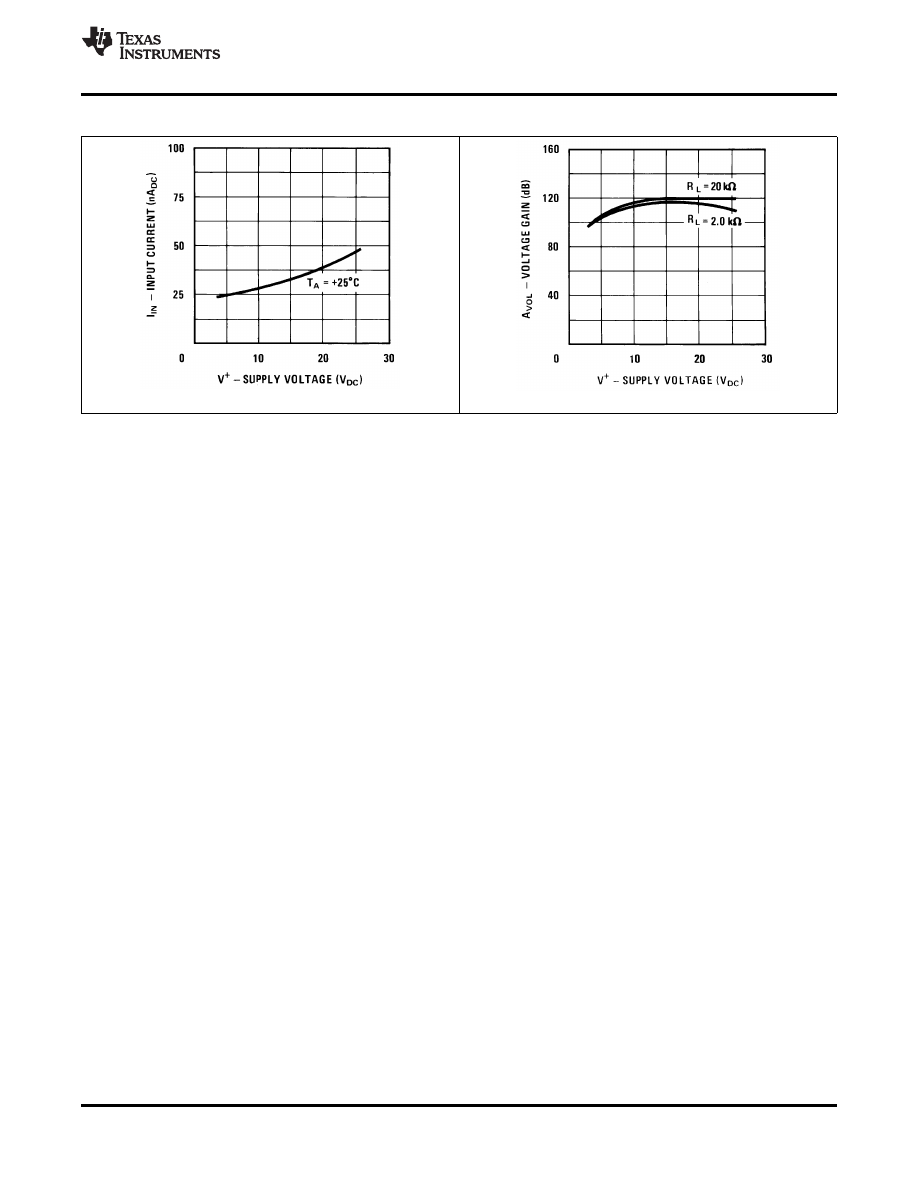
Typical Characteristics (continued)
Figure 13. Input Current (LM2902 Only)
Figure 14. Voltage Gain (LM2902 Only)
Copyright © 2000-2014, Texas Instruments Incorporated
11
Product Folder Links:
, , ,
SNOSBT3I - JANUARY 2000 - REVISED DECEMBER 2014
7 Detailed Description
7.1 Overview
The LM158 series are operational amplifiers which can operate with only a single power supply voltage, have
true-differential inputs, and remain in the linear mode with an input common-mode voltage of 0 V
DC
. These
amplifiers operate over a wide range of power supply voltage with little change in performance characteristics. At
25 °C amplifier operation is possible down to a minimum supply voltage of 2.3 V
DC
.
Large differential input voltages can be easily accommodated and, as input differential voltage protection diodes
are not needed, no large input currents result from large differential input voltages. The differential input voltage
may be larger than V
+
without damaging the device. Protection should be provided to prevent the input voltages
from going negative more than
-0.3 V
DC
(at 25 °C). An input clamp diode with a resistor to the IC input terminal
can be used.
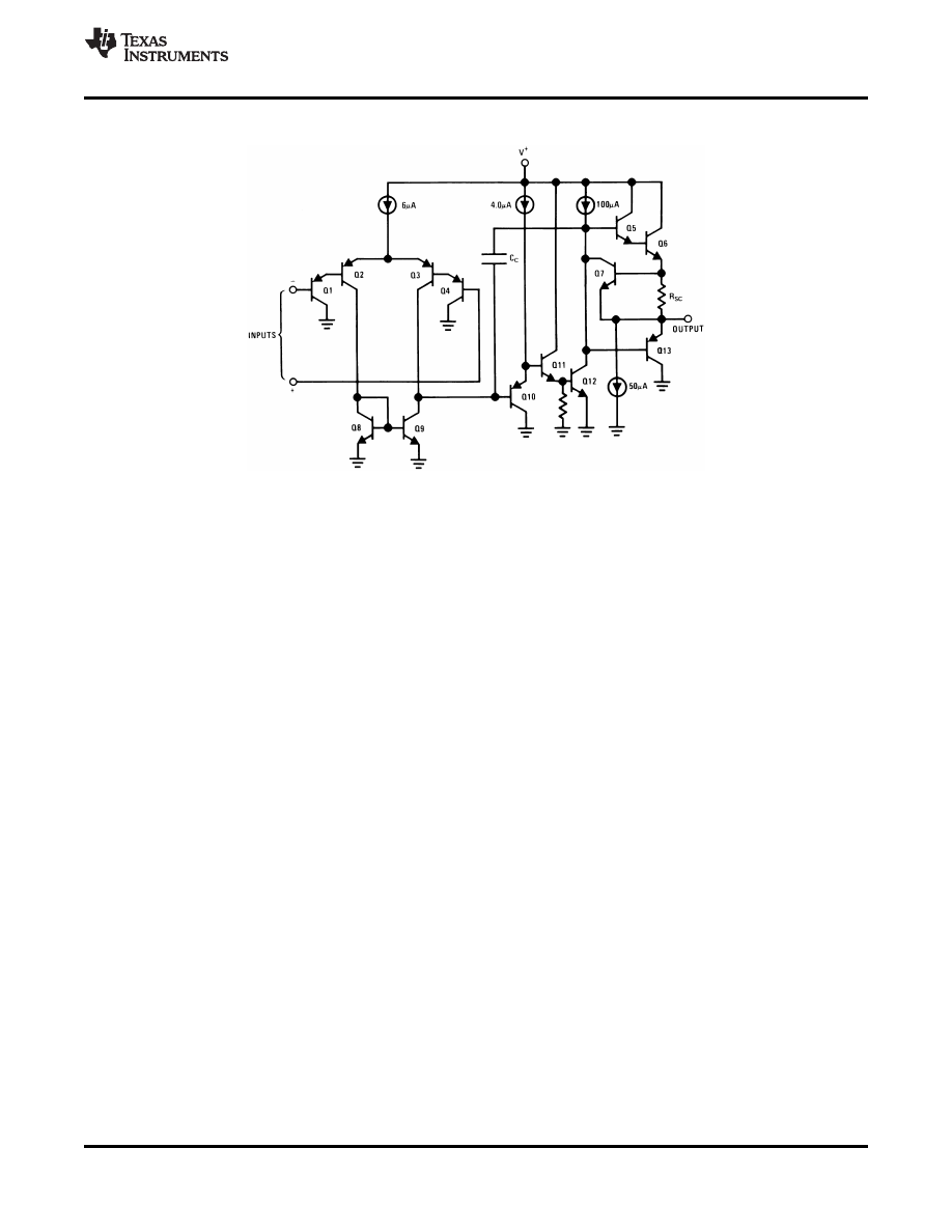
7.2 Functional Block Diagram
Figure 15. (Each Amplifier)
7.3 Feature Description
The amplifier's differential inputs consist of a non-inverting input (+IN) and an inverting input (-IN). The amplifer
amplifies only the difference in voltage between the two inpus, which is called the differential input voltage. The
output voltage of the op-amp Vout is given by Equation 1:
VOUT = AOL (IN+ - IN-)
where
AOL is the open-loop gain of the amplifier, typically around 100dB (100,000x, or 10uV per Volt).
(1)
To reduce the power supply current drain, the amplifiers have a class A output stage for small signal levels which
converts to class B in a large signal mode. This allows the amplifiers to both source and sink large output
currents. Therefore both NPN and PNP external current boost transistors can be used to extend the power
capability of the basic amplifiers. The output voltage needs to raise approximately 1 diode drop above ground to
bias the on-chip vertical PNP transistor for output current sinking applications.
For ac applications, where the load is capacitively coupled to the output of the amplifier, a resistor should be
used, from the output of the amplifier to ground to increase the class A bias current and prevent crossover
distortion. Where the load is directly coupled, as in dc applications, there is no crossover distortion.
Capacitive loads which are applied directly to the output of the amplifier reduce the loop stability margin. Values
of 50 pF can be accommodated using the worst-case non-inverting unity gain connection. Large closed loop
gains or resistive isolation should be used if larger load capacitance must be driven by the amplifier.
The bias network of the LM158 establishes a drain current which is independent of the magnitude of the power
supply voltage over the range of 3 V
DC
to 30 V
DC
.
Output short circuits either to ground or to the positive power supply should be of short time duration. Units can
be destroyed, not as a result of the short circuit current causing metal fusing, but rather due to the large increase
in IC chip power dissipation which will cause eventual failure due to excessive junction temperatures. Putting
direct short-circuits on more than one amplifier at a time will increase the total IC power dissipation to destructive
levels, if not properly protected with external dissipation limiting resistors in series with the output leads of the
amplifiers. The larger value of output source current which is available at 25 °C provides a larger output current
capability at elevated temperatures (see
than a standard IC op amp.
12
Copyright © 2000-2014, Texas Instruments Incorporated
Product Folder Links:
, ,
SNOSBT3I - JANUARY 2000 - REVISED DECEMBER 2014
7.4 Device Functional Modes
Figure 16. Schematic Diagram
The circuits presented in the
emphasize operation on only a single power
supply voltage. If complementary power supplies are available, all of the standard op-amp circuits can be used.
In general, introducing a pseudo-ground (a bias voltage reference of V
+
/2) will allow operation above and below
this value in single power supply systems. Many application circuits are shown which take advantage of the wide
input common-mode voltage range which includes ground. In most cases, input biasing is not required and input
voltages which range to ground can easily be accommodated.
Copyright © 2000-2014, Texas Instruments Incorporated
13
Product Folder Links:
, , ,
SNOSBT3I - JANUARY 2000 - REVISED DECEMBER 2014
8 Application and Implementation
NOTE
Information in the following applications sections is not part of the TI component
specification, and TI does not warrant its accuracy or completeness. TIs customers are
responsible for determining suitability of components for their purposes. Customers should
validate and test their design implementation to confirm system functionality.
8.1 Application Information
The LM158 family bring performance, economy, and ease-of-use to a wide variety of op-amp applications.
8.2 Typical Applications
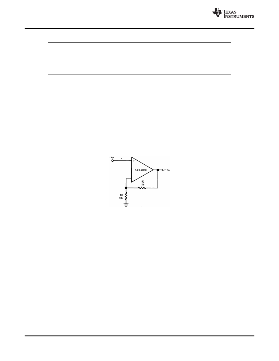
8.2.1 Noninverting DC Gain
shows a high input impedance non-inverting circuit. This circuit gives a closed-loop gain equal to the
ratio of the sum of R1 and R2 to R1 and a closed-loop 3 dB bandwidth equal to the amplifier unity-gain frequency
divided by the closed-loop gain. This design has the benefit of a very high input impedance, which is equal to the
differential input impedance multiplied by loop gain. (Open loop gain/Closed loop gain.) In DC coupled
applications, input impedance is not as important as input current and its voltage drop across the source
resistance. Note that the amplifier output will go into saturation if the input is allowed to float. This may be
important if the amplifier must be switched from source to source.
*R not needed due to temperature independent I
IN
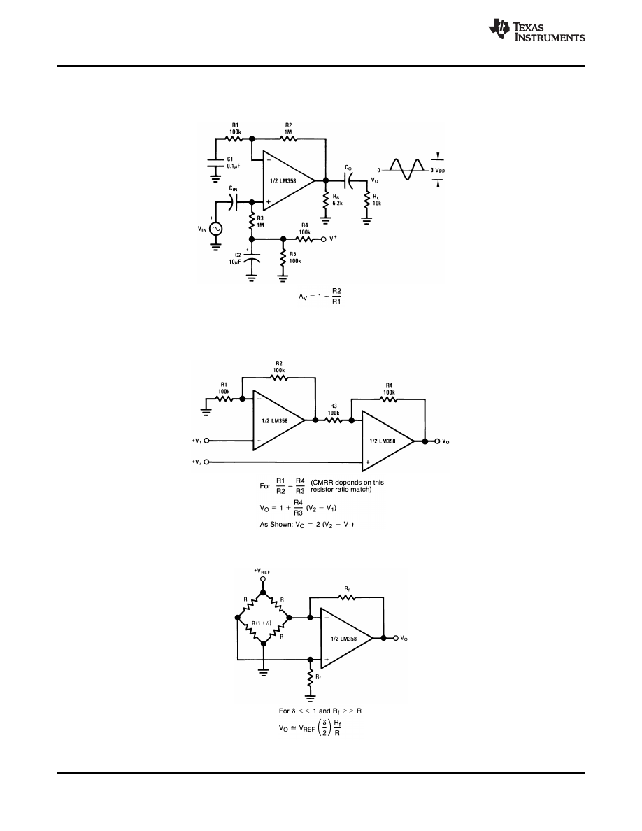
Figure 17. Non-Inverting DC Gain (0-V Output)
8.2.1.1 Design Requirements
For this example application, the supply voltage is +5V, and 100x ±5% of noninverting gain is necessary. Signal
input impedance is approx 10k
Ω.
8.2.1.2 Detailed Design Procedure
Using the equation for a non-inverting amplifier configuration ; G = 1+ R2/R1, set R1 to 10k
Ω, and R2 to 99x the
value of R1, which would be 990k
Ω. Replacing the 990kΩ with a 1MΩ will result in a gain of 101, which is within
the desired gain tolerance.
The gain-frequency characteristic of the amplifier and its feedback network must be such that oscillation does not
occur. To meet this condition, the phase shift through amplifier and feedback network must never exceed 180 °
for any frequency where the gain of the amplifier and its feedback network is greater than unity. In practical
applications, the phase shift should not approach 180 ° since this is the situation of conditional stability. Obviously
the most critical case occurs when the attenuation of the feedback network is zero.
14
Copyright © 2000-2014, Texas Instruments Incorporated
Product Folder Links:
, ,
SNOSBT3I - JANUARY 2000 - REVISED DECEMBER 2014
Typical Applications (continued)
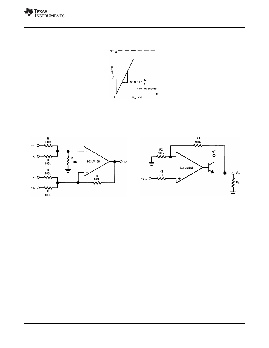
8.2.1.3 Application Curve
Figure 18. Transfer Curve for Non-Inverting Configuration
8.2.2 System Examples
8.2.2.1 Typical Single-Supply Applications
(V
+
= 5.0 V
DC
)
V
O
= 0 V
DC
for V
IN
= 0 V
DC
Where: V
O
= V
1
+ V
2
- V
3
- V
4
A
V
= 10
(V
1
+ V
2
)
≥ (V
3
+ V
4
) to keep V
O
> 0 V
DC
Figure 19. DC Summing Amplifier
Figure 20. Power Amplifier
(V
IN'S
≥ 0 V
DC
and V
O
≥ 0 V
DC
)
Copyright © 2000-2014, Texas Instruments Incorporated
15
Product Folder Links:
, , ,
SNOSBT3I - JANUARY 2000 - REVISED DECEMBER 2014
Typical Applications (continued)
(V
+
= 5.0 V
DC
)
f
o
= 1 kHz
Q = 50
A
v
= 100 (40 dB)
Figure 21. BI-QUAD RC Active Bandpass Filter
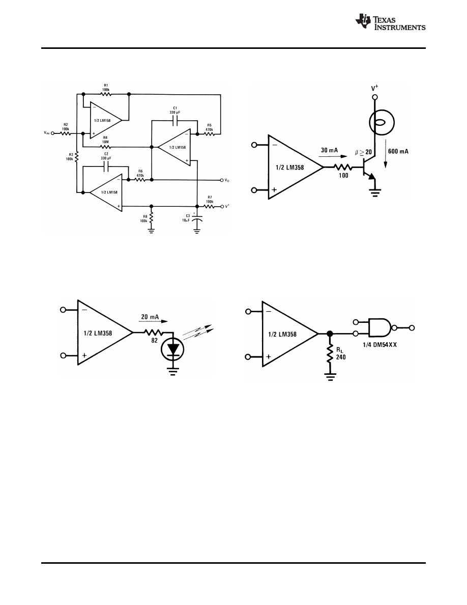
Figure 22. Lamp Driver
Figure 23. LED Driver
Figure 24. Driving TTL
16
Copyright © 2000-2014, Texas Instruments Incorporated
Product Folder Links:
, ,
SNOSBT3I - JANUARY 2000 - REVISED DECEMBER 2014
Typical Applications (continued)
(V
+
= 5.0 V
DC
)
V
O
= V
IN
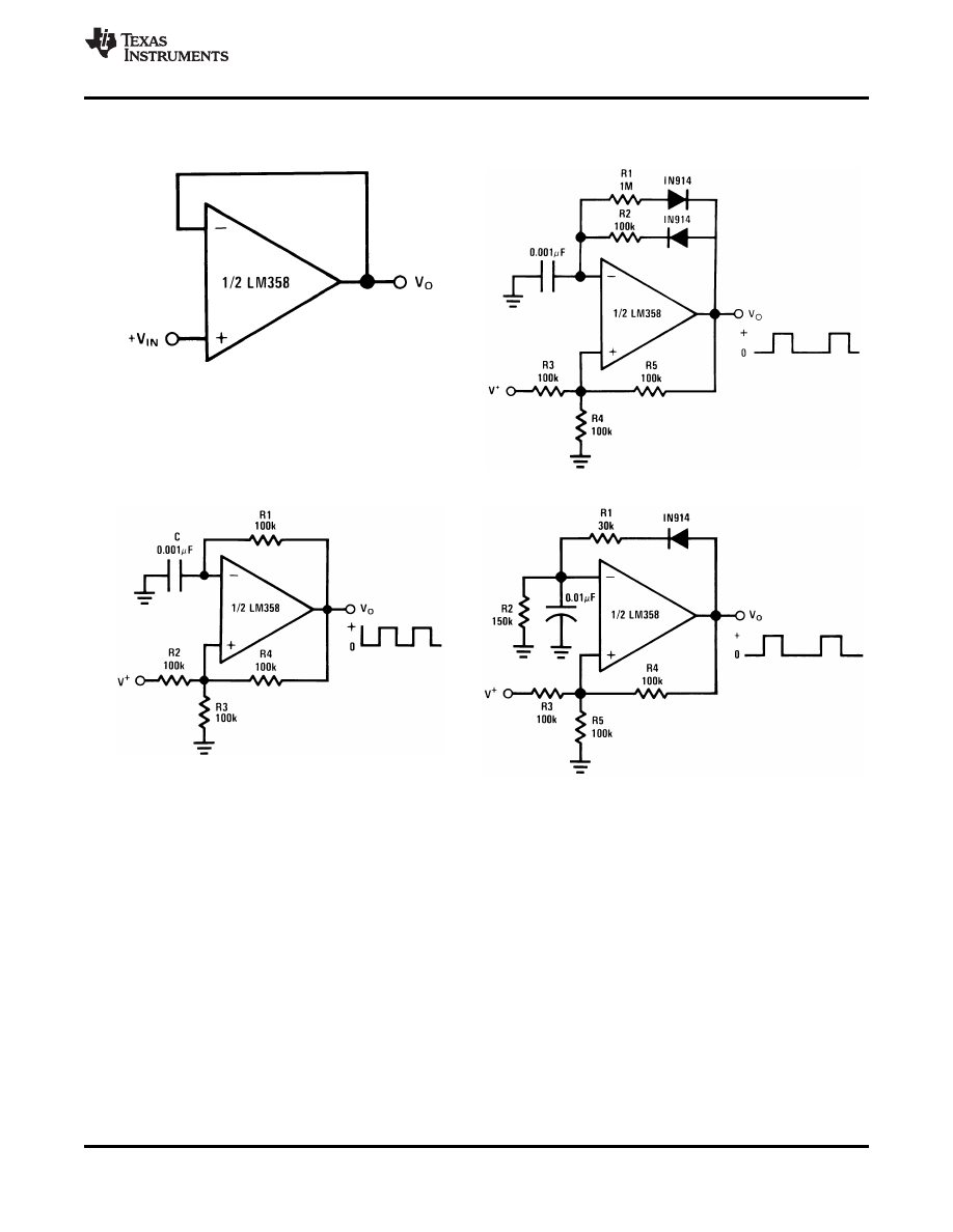
Figure 25. Voltage Follower
Figure 26. Pulse Generator
Figure 27. Squarewave Oscillator
Figure 28. Pulse Generator
Copyright © 2000-2014, Texas Instruments Incorporated
17
Product Folder Links:
, , ,
SNOSBT3I - JANUARY 2000 - REVISED DECEMBER 2014
Typical Applications (continued)
(V
+
= 5.0 V
DC
)
HIGH Z
IN
I
O
= 1 amp/volt V
IN
LOW Z
OUT
(Increase R
E
for I
O
small)
Figure 29. Low Drift Peak Detector
Figure 30. High Compliance Current Sink
*WIDE CONTROL VOLTAGE RANGE: 0 V
DC
≤ V
C
≤
2 (V
+
-1.5V
DC
)
Figure 31. Comparator with Hysteresis
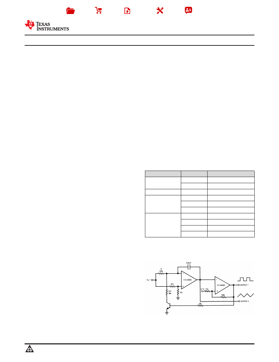
Figure 32. Voltage Controlled Oscillator (VCO)
18
Copyright © 2000-2014, Texas Instruments Incorporated
Product Folder Links:
, ,
SNOSBT3I - JANUARY 2000 - REVISED DECEMBER 2014
Typical Applications (continued)
(V
+
= 5.0 V
DC
)
f
o
= 1 kHz
Q = 1
A
V
= 2
Figure 33. Ground Referencing a Differential Input
Figure 34. DC Coupled Low-Pass RC Active Filter
Signal
f
o
= 1 kHz
Q = 25
Figure 35. Bandpass Active Filter
Figure 36. Photo Voltaic-Cell Amplifier
Copyright © 2000-2014, Texas Instruments Incorporated
19
Product Folder Links:
, , ,
SNOSBT3I - JANUARY 2000 - REVISED DECEMBER 2014
Typical Applications (continued)
(V
+
= 5.0 V
DC
)
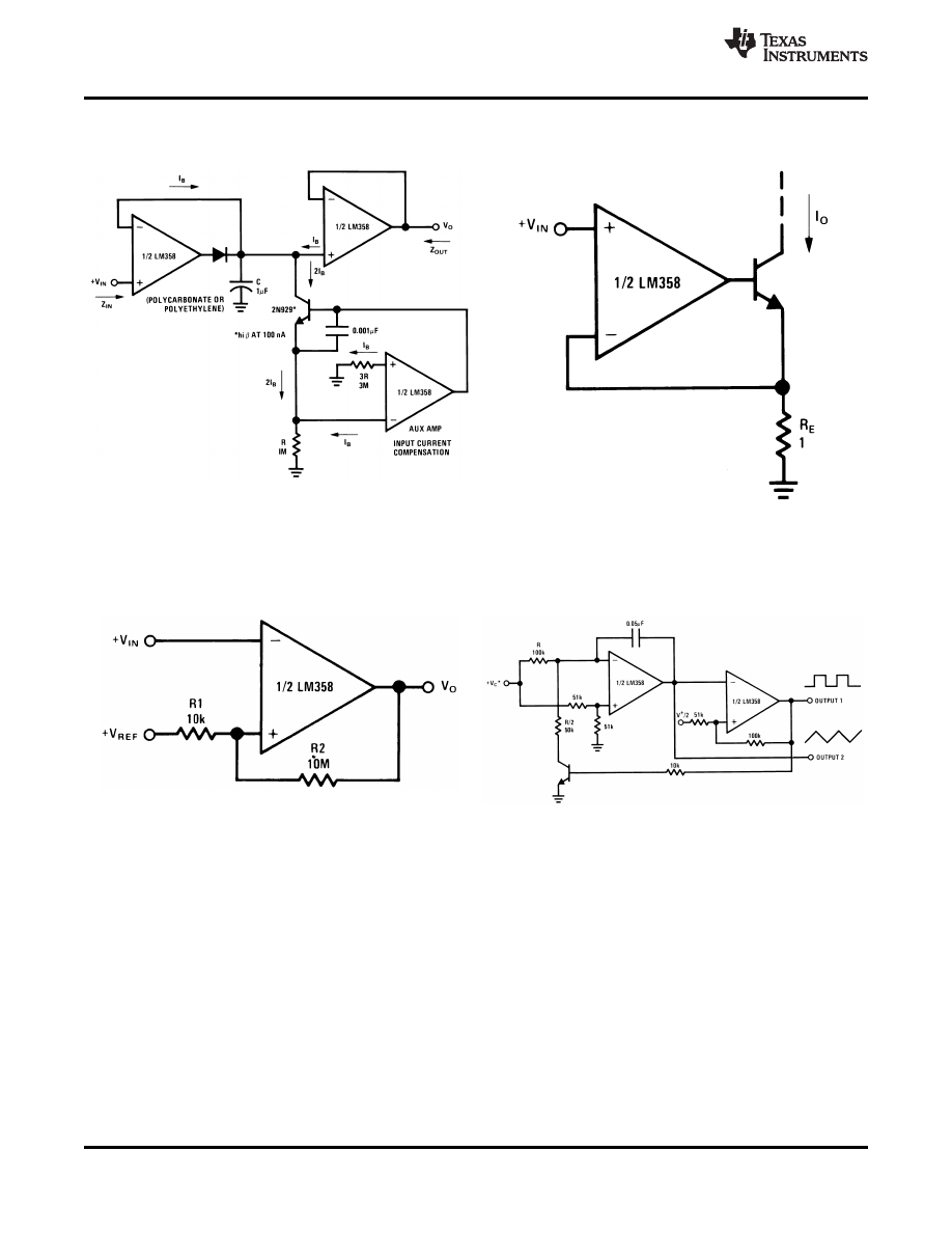
Figure 37. Using Symmetrical Amplifiers to Reduce Input Current (General Concept)
Figure 38. Fixed Current Sources
20
Copyright © 2000-2014, Texas Instruments Incorporated
Product Folder Links:
, ,
SNOSBT3I - JANUARY 2000 - REVISED DECEMBER 2014
Typical Applications (continued)
(V
+
= 5.0 V
DC
)
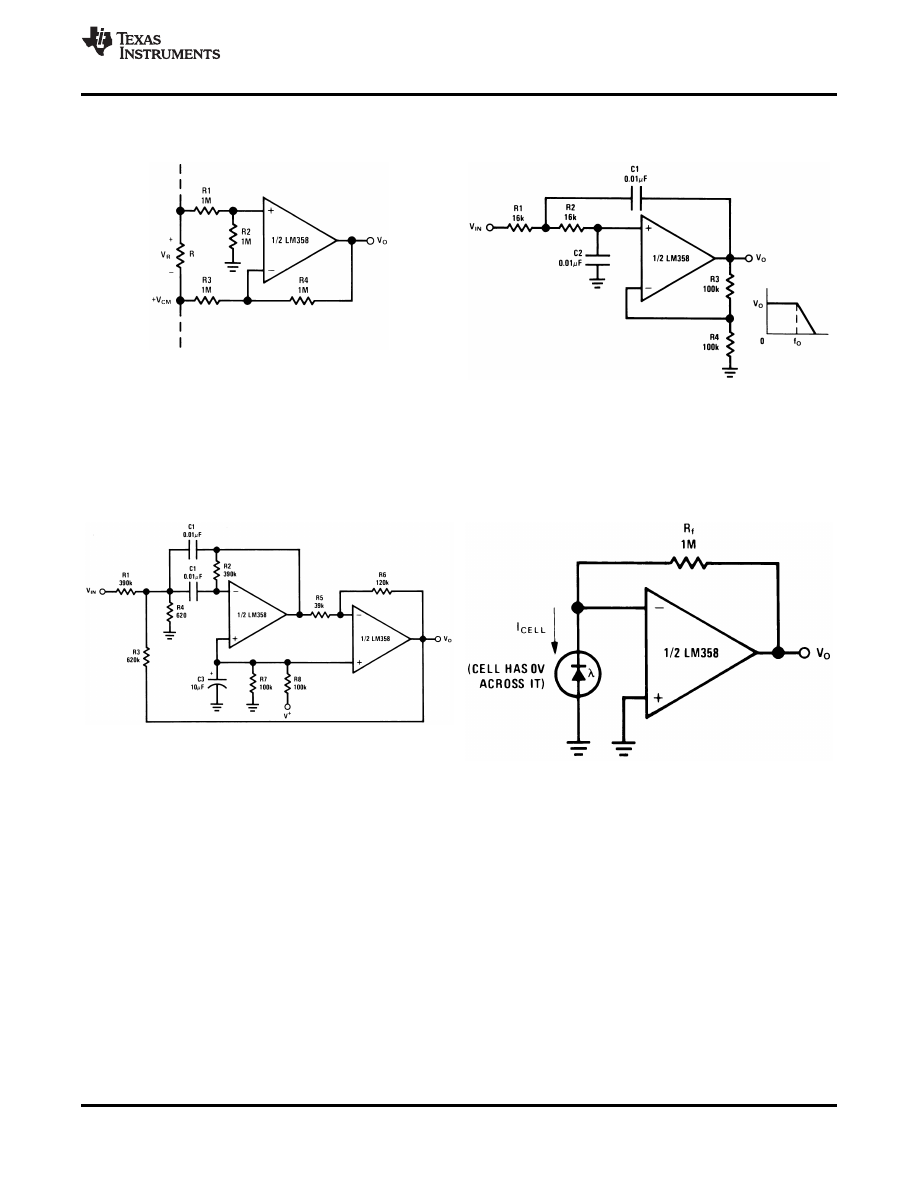
*(Increase R1 for I
L
small)
V
L
≤ V
+
-2V
Figure 39. Current Monitor
Figure 40. AC Coupled Inverting Amplifier
Copyright © 2000-2014, Texas Instruments Incorporated
21
Product Folder Links:
, , ,
SNOSBT3I - JANUARY 2000 - REVISED DECEMBER 2014
Typical Applications (continued)
(V
+
= 5.0 V
DC
)
A
v
= 11 (As Shown)
Figure 41. AC Coupled Non-Inverting Amplifier
Figure 42. High Input Z, DC Differential Amplifier
Figure 43. Bridge Current Amplifier
22
Copyright © 2000-2014, Texas Instruments Incorporated
Product Folder Links:
, ,
SNOSBT3I - JANUARY 2000 - REVISED DECEMBER 2014
Typical Applications (continued)
(V
+
= 5.0 V
DC
)
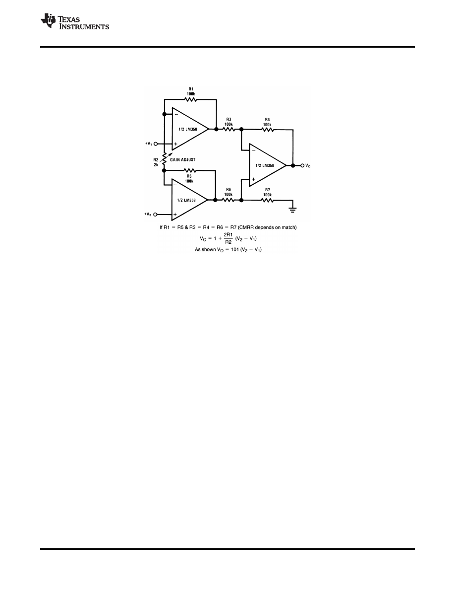
Figure 44. High Input Z Adjustable-Gain DC Instrumentation Amplifier
Copyright © 2000-2014, Texas Instruments Incorporated
23
Product Folder Links:
, , ,
SNOSBT3I - JANUARY 2000 - REVISED DECEMBER 2014
9 Power Supply Recommendations
For proper operation, the power supplies must be properly decoupled. For decoupling the supply pins it is
suggested that 10 nF capacitors be placed as close as possible to the op-amp power supply pins. For single
supply, place a capacitor between V+ and V
-supply leads. For dual supplies, place one capacitor between
V+ and ground, and one capacitor between V- and ground.
Precautions should be taken to insure that the power supply for the integrated circuit never becomes
reversed in polarity or that the unit is not inadvertently installed backwards in a test socket as an unlimited
current surge through the resulting forward diode within the IC could cause fusing of the internal conductors
and result in a destroyed unit.
10 Layout
10.1 Layout Guidelines
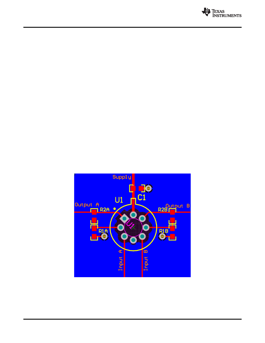
For single-ended supply configurations, the V+ pin should be bypassed to ground with a low ESR capacitor. The
optimum placement is closest to the V+ pin. Care should be taken to minimize the loop area formed by the
bypass capacitor connection between V+ and ground. The ground pin should be connected to the PCB ground
plane at the pin of the device. The feedback components should be placed as close to the device as possible to
minimize stray parasitics.
For dual supply configurations, both the V+ pin and V- pin should be bypassed to ground with a low ESR
capacitor. The optimum placement is closest to the corresponding supply pin. Care should be taken to minimize
the loop area formed by the bypass capacitor connection between V+ or V- and ground. The feedback
components should be placed as close to the device as possible to minimize stray parasitics.
For both configurations, as ground plane underneath the device is recommended.
10.2 Layout Example
Figure 45. Layout Example
24
Copyright © 2000-2014, Texas Instruments Incorporated
Product Folder Links:
, ,
SNOSBT3I - JANUARY 2000 - REVISED DECEMBER 2014
11 Device and Documentation Support
11.1 Related Links
The table below lists quick access links. Categories include technical documents, support and community
resources, tools and software, and quick access to sample or buy.
Table 1. Related Links
TECHNICAL
TOOLS &
SUPPORT &
PARTS
PRODUCT FOLDER
SAMPLE & BUY
DOCUMENTS
SOFTWARE
COMMUNITY
LM158-N
LM258-N
LM2904-N
LM358-N
11.2 Trademarks
All trademarks are the property of their respective owners.
11.3 Electrostatic Discharge Caution
These devices have limited built-in ESD protection. The leads should be shorted together or the device placed in conductive foam
during storage or handling to prevent electrostatic damage to the MOS gates.
11.4 Glossary
TI Glossary.
This glossary lists and explains terms, acronyms, and definitions.
12 Mechanical, Packaging, and Orderable Information
The following pages include mechanical, packaging, and orderable information. This information is the most
current data available for the designated devices. This data is subject to change without notice and revision of
this document. For browser-based versions of this data sheet, refer to the left-hand navigation.
Copyright © 2000-2014, Texas Instruments Incorporated
25
Product Folder Links:
PACKAGE OPTION ADDENDUM
www.ti.com
19-Mar-2015
Addendum-Page 1
PACKAGING INFORMATION
Orderable Device
Status
(1)
Package Type Package
Drawing
Pins Package
Qty
Eco Plan
(2)
Lead/Ball Finish
(6)
MSL Peak Temp
(3)
Op Temp ( °C)
Device Marking
(4/5)
Samples
LM158AH
ACTIVE
TO-99
LMC
8
500
TBD
Call TI
Call TI
-55 to 125
( LM158AH ~
LM158AH)
LM158AH/NOPB
ACTIVE
TO-99
LMC
8
500
Green (RoHS
& no Sb/Br)
Call TI
Level-1-NA-UNLIM
-55 to 125
( LM158AH ~
LM158AH)
LM158H
ACTIVE
TO-99
LMC
8
500
TBD
Call TI
Call TI
-55 to 125
( LM158H ~ LM158H)
LM158H/NOPB
ACTIVE
TO-99
LMC
8
500
Green (RoHS
& no Sb/Br)
Call TI
Level-1-NA-UNLIM
-55 to 125
( LM158H ~ LM158H)
LM158J
ACTIVE
CDIP
NAB
8
40
TBD
Call TI
Call TI
-55 to 125
LM158J
LM258H
ACTIVE
TO-99
LMC
8
500
TBD
Call TI
Call TI
-25 to 85
( LM258H ~ LM258H)
LM258H/NOPB
ACTIVE
TO-99
LMC
8
500
Green (RoHS
& no Sb/Br)
Call TI
Level-1-NA-UNLIM
-25 to 85
( LM258H ~ LM258H)
LM2904ITP/NOPB
ACTIVE
DSBGA
YPB
8
250
Green (RoHS
& no Sb/Br)
SNAGCU
Level-1-260C-UNLIM
-40 to 85
A
09
LM2904ITPX/NOPB
ACTIVE
DSBGA
YPB
8
3000
Green (RoHS
& no Sb/Br)
SNAGCU
Level-1-260C-UNLIM
-40 to 85
A
09
LM2904M
NRND
SOIC
D
8
95
TBD
Call TI
Call TI
-40 to 85
LM
2904M
LM2904M/NOPB
ACTIVE
SOIC
D
8
95
Green (RoHS
& no Sb/Br)
CU SN
Level-1-260C-UNLIM
-40 to 85
LM
2904M
LM2904MX
NRND
SOIC
D
8
2500
TBD
Call TI
Call TI
-40 to 85
LM
2904M
LM2904MX/NOPB
ACTIVE
SOIC
D
8
2500
Green (RoHS
& no Sb/Br)
CU SN
Level-1-260C-UNLIM
-40 to 85
LM
2904M
LM2904N/NOPB
ACTIVE
PDIP
P
8
40
Green (RoHS
& no Sb/Br)
CU SN
Level-1-NA-UNLIM
-40 to 85
LM
2904N
LM358AM
NRND
SOIC
D
8
95
TBD
Call TI
Call TI
0 to 70
LM
358AM
LM358AM/NOPB
ACTIVE
SOIC
D
8
95
Green (RoHS
& no Sb/Br)
CU SN
Level-1-260C-UNLIM
0 to 70
LM
358AM
LM358AMX
NRND
SOIC
D
8
2500
TBD
Call TI
Call TI
0 to 70
LM
358AM
PACKAGE OPTION ADDENDUM
www.ti.com
19-Mar-2015
Addendum-Page 2
Orderable Device
Status
(1)
Package Type Package
Drawing
Pins Package
Qty
Eco Plan
(2)
Lead/Ball Finish
(6)
MSL Peak Temp
(3)
Op Temp ( °C)
Device Marking
(4/5)
Samples
LM358AMX/NOPB
ACTIVE
SOIC
D
8
2500
Green (RoHS
& no Sb/Br)
CU SN
Level-1-260C-UNLIM
0 to 70
LM
358AM
LM358AN/NOPB
ACTIVE
PDIP
P
8
40
Green (RoHS
& no Sb/Br)
CU SN
Level-1-NA-UNLIM
0 to 70
LM
358AN
LM358H/NOPB
ACTIVE
TO-99
LMC
8
500
Green (RoHS
& no Sb/Br)
Call TI
Level-1-NA-UNLIM
0 to 70
( LM358H ~ LM358H)
LM358M
NRND
SOIC
D
8
95
TBD
Call TI
Call TI
0 to 70
LM
358M
LM358M/NOPB
ACTIVE
SOIC
D
8
95
Green (RoHS
& no Sb/Br)
CU SN
Level-1-260C-UNLIM
0 to 70
LM
358M
LM358MX
NRND
SOIC
D
8
2500
TBD
Call TI
Call TI
0 to 70
LM
358M
LM358MX/NOPB
ACTIVE
SOIC
D
8
2500
Green (RoHS
& no Sb/Br)
CU SN
Level-1-260C-UNLIM
0 to 70
LM
358M
LM358N/NOPB
ACTIVE
PDIP
P
8
40
Green (RoHS
& no Sb/Br)
CU SN
Level-1-NA-UNLIM
0 to 70
LM
358N
LM358TP/NOPB
ACTIVE
DSBGA
YPB
8
250
Green (RoHS
& no Sb/Br)
SNAGCU
Level-1-260C-UNLIM
0 to 70
A
07
LM358TPX/NOPB
ACTIVE
DSBGA
YPB
8
3000
Green (RoHS
& no Sb/Br)
SNAGCU
Level-1-260C-UNLIM
0 to 70
A
07
(1)
The marketing status values are defined as follows:
ACTIVE: Product device recommended for new designs.
LIFEBUY: TI has announced that the device will be discontinued, and a lifetime-buy period is in effect.
NRND: Not recommended for new designs. Device is in production to support existing customers, but TI does not recommend using this part in a new design.
PREVIEW: Device has been announced but is not in production. Samples may or may not be available.
OBSOLETE: TI has discontinued the production of the device.
(2)
Eco Plan - The planned eco-friendly classification: Pb-Free (RoHS), Pb-Free (RoHS Exempt), or Green (RoHS & no Sb/Br) - please check
for the latest availability
information and additional product content details.
TBD: The Pb-Free/Green conversion plan has not been defined.
Pb-Free (RoHS): TI's terms "Lead-Free" or "Pb-Free" mean semiconductor products that are compatible with the current RoHS requirements for all 6 substances, including the requirement that
lead not exceed 0.1% by weight in homogeneous materials. Where designed to be soldered at high temperatures, TI Pb-Free products are suitable for use in specified lead-free processes.
Pb-Free (RoHS Exempt): This component has a RoHS exemption for either 1) lead-based flip-chip solder bumps used between the die and package, or 2) lead-based die adhesive used between
the die and leadframe. The component is otherwise considered Pb-Free (RoHS compatible) as defined above.
Green (RoHS & no Sb/Br): TI defines "Green" to mean Pb-Free (RoHS compatible), and free of Bromine (Br) and Antimony (Sb) based flame retardants (Br or Sb do not exceed 0.1% by weight
in homogeneous material)
PACKAGE OPTION ADDENDUM
www.ti.com
19-Mar-2015
Addendum-Page 3
(3)
MSL, Peak Temp. - The Moisture Sensitivity Level rating according to the JEDEC industry standard classifications, and peak solder temperature.
(4)
There may be additional marking, which relates to the logo, the lot trace code information, or the environmental category on the device.
(5)
Multiple Device Markings will be inside parentheses. Only one Device Marking contained in parentheses and separated by a "~" will appear on a device. If a line is indented then it is a continuation
of the previous line and the two combined represent the entire Device Marking for that device.
(6)
Lead/Ball Finish - Orderable Devices may have multiple material finish options. Finish options are separated by a vertical ruled line. Lead/Ball Finish values may wrap to two lines if the finish
value exceeds the maximum column width.
Important Information and Disclaimer:The information provided on this page represents TI's knowledge and belief as of the date that it is provided. TI bases its knowledge and belief on information
provided by third parties, and makes no representation or warranty as to the accuracy of such information. Efforts are underway to better integrate information from third parties. TI has taken and
continues to take reasonable steps to provide representative and accurate information but may not have conducted destructive testing or chemical analysis on incoming materials and chemicals.
TI and TI suppliers consider certain information to be proprietary, and thus CAS numbers and other limited information may not be available for release.
In no event shall TI's liability arising out of such information exceed the total purchase price of the TI part(s) at issue in this document sold by TI to Customer on an annual basis.
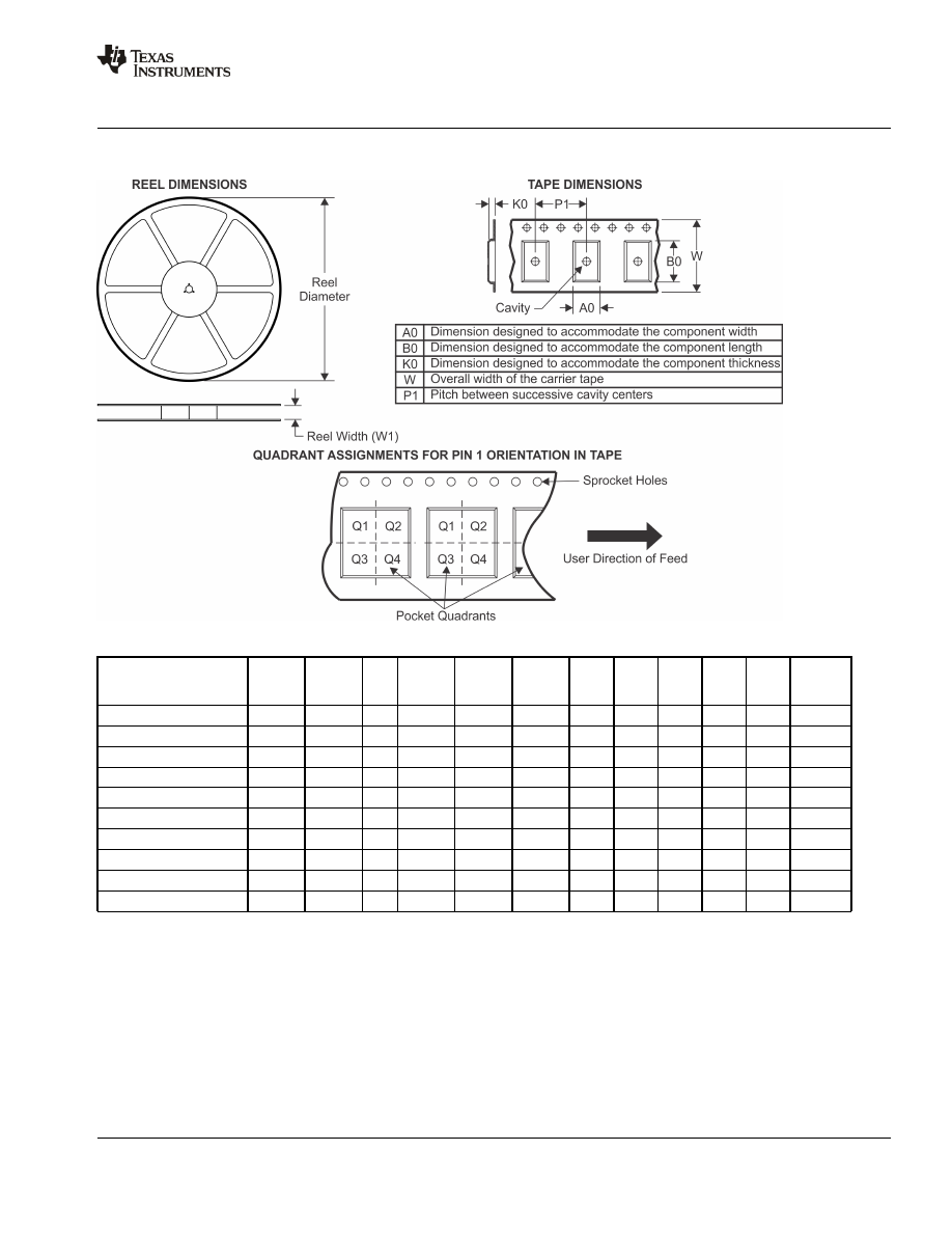
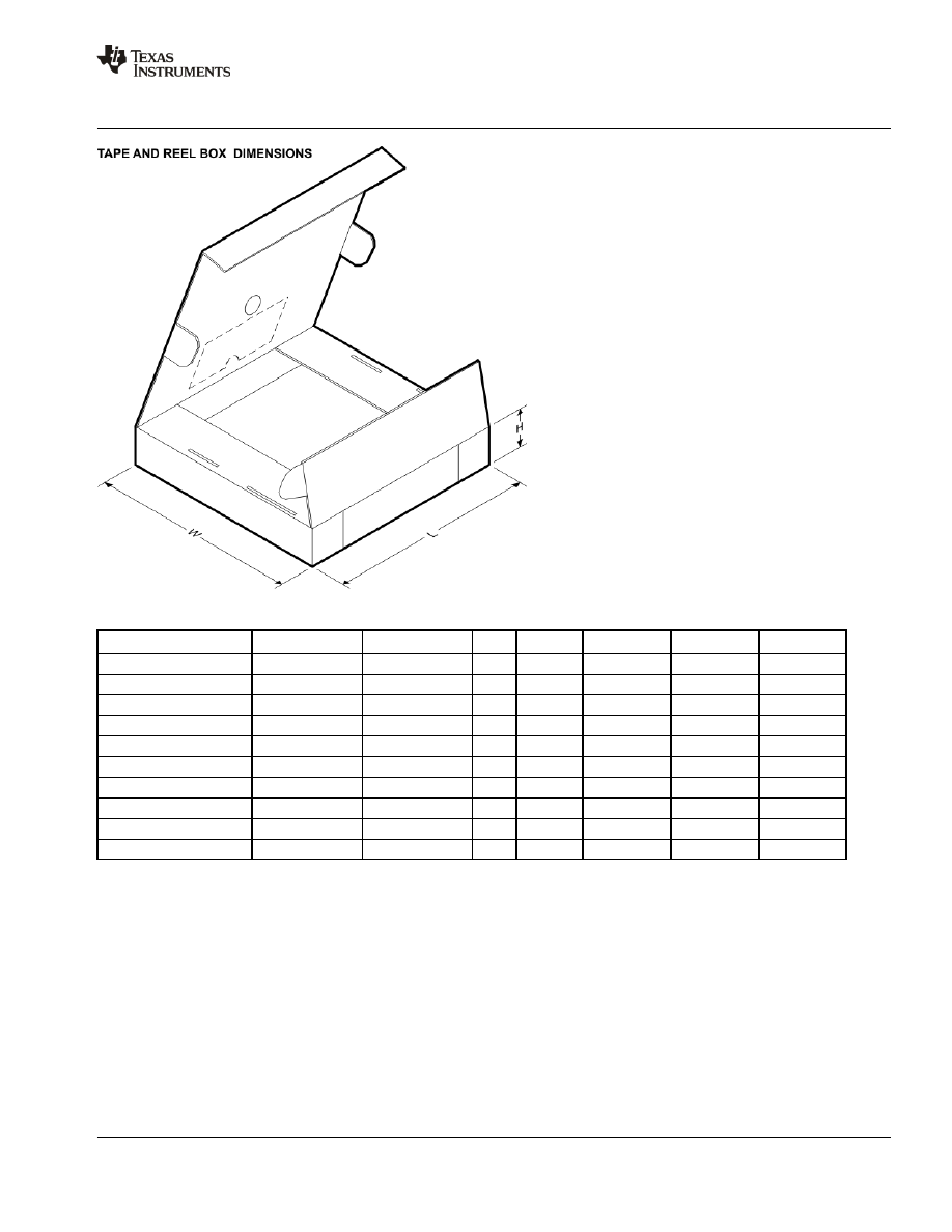
TAPE AND REEL INFORMATION
*All dimensions are nominal
Device
Package
Type
Package
Drawing
Pins
SPQ
Reel
Diameter
(mm)
Reel
Width
W1 (mm)
A0
(mm)
B0
(mm)
K0
(mm)
P1
(mm)
W
(mm)
Pin1
Quadrant
LM2904ITP/NOPB
DSBGA
YPB
8
250
178.0
8.4
1.5
1.5
0.66
4.0
8.0
Q1
LM2904ITPX/NOPB
DSBGA
YPB
8
3000
178.0
8.4
1.5
1.5
0.66
4.0
8.0
Q1
LM2904MX
SOIC
D
8
2500
330.0
12.4
6.5
5.4
2.0
8.0
12.0
Q1
LM2904MX/NOPB
SOIC
D
8
2500
330.0
12.4
6.5
5.4
2.0
8.0
12.0
Q1
LM358AMX
SOIC
D
8
2500
330.0
12.4
6.5
5.4
2.0
8.0
12.0
Q1
LM358AMX/NOPB
SOIC
D
8
2500
330.0
12.4
6.5
5.4
2.0
8.0
12.0
Q1
LM358MX
SOIC
D
8
2500
330.0
12.4
6.5
5.4
2.0
8.0
12.0
Q1
LM358MX/NOPB
SOIC
D
8
2500
330.0
12.4
6.5
5.4
2.0
8.0
12.0
Q1
LM358TP/NOPB
DSBGA
YPB
8
250
178.0
8.4
1.5
1.5
0.66
4.0
8.0
Q1
LM358TPX/NOPB
DSBGA
YPB
8
3000
178.0
8.4
1.5
1.5
0.66
4.0
8.0
Q1
PACKAGE MATERIALS INFORMATION
www.ti.com
7-Oct-2014
Pack Materials-Page 1
*All dimensions are nominal
Device
Package Type
Package Drawing
Pins
SPQ
Length (mm)
Width (mm)
Height (mm)
LM2904ITP/NOPB
DSBGA
YPB
8
250
210.0
185.0
35.0
LM2904ITPX/NOPB
DSBGA
YPB
8
3000
210.0
185.0
35.0
LM2904MX
SOIC
D
8
2500
367.0
367.0
35.0
LM2904MX/NOPB
SOIC
D
8
2500
367.0
367.0
35.0
LM358AMX
SOIC
D
8
2500
367.0
367.0
35.0
LM358AMX/NOPB
SOIC
D
8
2500
367.0
367.0
35.0
LM358MX
SOIC
D
8
2500
367.0
367.0
35.0
LM358MX/NOPB
SOIC
D
8
2500
367.0
367.0
35.0
LM358TP/NOPB
DSBGA
YPB
8
250
210.0
185.0
35.0
LM358TPX/NOPB
DSBGA
YPB
8
3000
210.0
185.0
35.0
PACKAGE MATERIALS INFORMATION
www.ti.com
7-Oct-2014
Pack Materials-Page 2
MECHANICAL DATA
NAB0008A
www.ti.com
J08A (Rev M)
MECHANICAL DATA
YPB0008
www.ti.com
TPA08XXX (Rev A)
0.5 ±0.045
D
E
4215100/A 12/12
A. All linear dimensions are in millimeters. Dimensioning and tolerancing per ASME Y14.5M-1994.
B. This drawing is subject to change without notice.
NOTES:
D: Max =
E: Max =
1.337 mm, Min =
1.337 mm, Min =
1.276 mm
1.276 mm

IMPORTANT NOTICE
Texas Instruments Incorporated and its subsidiaries (TI) reserve the right to make corrections, enhancements, improvements and other
changes to its semiconductor products and services per JESD46, latest issue, and to discontinue any product or service per JESD48, latest
issue. Buyers should obtain the latest relevant information before placing orders and should verify that such information is current and
complete. All semiconductor products (also referred to herein as components) are sold subject to TIs terms and conditions of sale
supplied at the time of order acknowledgment.
TI warrants performance of its components to the specifications applicable at the time of sale, in accordance with the warranty in TIs terms
and conditions of sale of semiconductor products. Testing and other quality control techniques are used to the extent TI deems necessary
to support this warranty. Except where mandated by applicable law, testing of all parameters of each component is not necessarily
performed.
TI assumes no liability for applications assistance or the design of Buyers products. Buyers are responsible for their products and
applications using TI components. To minimize the risks associated with Buyers products and applications, Buyers should provide
adequate design and operating safeguards.
TI does not warrant or represent that any license, either express or implied, is granted under any patent right, copyright, mask work right, or
other intellectual property right relating to any combination, machine, or process in which TI components or services are used. Information
published by TI regarding third-party products or services does not constitute a license to use such products or services or a warranty or
endorsement thereof. Use of such information may require a license from a third party under the patents or other intellectual property of the
third party, or a license from TI under the patents or other intellectual property of TI.
Reproduction of significant portions of TI information in TI data books or data sheets is permissible only if reproduction is without alteration
and is accompanied by all associated warranties, conditions, limitations, and notices. TI is not responsible or liable for such altered
documentation. Information of third parties may be subject to additional restrictions.
Resale of TI components or services with statements different from or beyond the parameters stated by TI for that component or service
voids all express and any implied warranties for the associated TI component or service and is an unfair and deceptive business practice.
TI is not responsible or liable for any such statements.
Buyer acknowledges and agrees that it is solely responsible for compliance with all legal, regulatory and safety-related requirements
concerning its products, and any use of TI components in its applications, notwithstanding any applications-related information or support
that may be provided by TI. Buyer represents and agrees that it has all the necessary expertise to create and implement safeguards which
anticipate dangerous consequences of failures, monitor failures and their consequences, lessen the likelihood of failures that might cause
harm and take appropriate remedial actions. Buyer will fully indemnify TI and its representatives against any damages arising out of the use
of any TI components in safety-critical applications.
In some cases, TI components may be promoted specifically to facilitate safety-related applications. With such components, TIs goal is to
help enable customers to design and create their own end-product solutions that meet applicable functional safety standards and
requirements. Nonetheless, such components are subject to these terms.
No TI components are authorized for use in FDA Class III (or similar life-critical medical equipment) unless authorized officers of the parties
have executed a special agreement specifically governing such use.
Only those TI components which TI has specifically designated as military grade or enhanced plastic are designed and intended for use in
military/aerospace applications or environments. Buyer acknowledges and agrees that any military or aerospace use of TI components
which have not been so designated is solely at the Buyer's risk, and that Buyer is solely responsible for compliance with all legal and
regulatory requirements in connection with such use.
TI has specifically designated certain components as meeting ISO/TS16949 requirements, mainly for automotive use. In any case of use of
non-designated products, TI will not be responsible for any failure to meet ISO/TS16949.
Products
Applications
Audio
Automotive and Transportation
Amplifiers
Communications and Telecom
Data Converters
Computers and Peripherals
DLP ® Products
Consumer Electronics
DSP
Energy and Lighting
Clocks and Timers
Industrial
Interface
Medical
Logic
Security
Power Mgmt
Space, Avionics and Defense
Microcontrollers
Video and Imaging
RFID
OMAP Applications Processors
TI E2E Community
Wireless Connectivity
Mailing Address: Texas Instruments, Post Office Box 655303, Dallas, Texas 75265
Copyright © 2016, Texas Instruments Incorporated
Document Outline

