| Secciones |
|---|
| Foros Electrónica |
|
|
| Boletines de correo |
 |
SNAS546C - DECEMBER 1994 - REVISED APRIL 2013
LM380 2.5W Audio Power Amplifier
Check for Samples:
1
FEATURES
DESCRIPTION
The LM380 is a power audio amplifier for consumer
Wide Supply Voltage Range: 10V-22V
applications. In order to hold system cost to a
Low Quiescent Power Drain: 0.13W (V
S
= 18V)
minimum, gain is internally fixed at 34 dB. A unique
Voltage Gain Fixed at 50
input stage allows ground referenced input signals.
The output automatically self-centers to one-half the
High Peak Current Capability: 1.3A
supply voltage.
Input Referenced to GND
The output is short circuit proof with internal thermal
High Input Impedance: 150k
Ω¦
limiting. The package outline is standard dual-in-line.
Low Distortion
The LM380N uses a copper lead frame. The center
Quiescent Output Voltage is at One-Half of the
three pins on either side comprise a heat sink. This
Supply Voltage
makes the device easy to use in standard PC layouts.
Standard Dual-In-Line Package
Uses
include
simple
phonograph
amplifiers,
intercoms, line drivers, teaching machine outputs,
alarms, ultrasonic drivers, TV sound systems, AM-FM
radio, small servo drivers, power converters, etc.
A selected part for more power on higher supply
voltages is available as the LM384. For more
information see
.
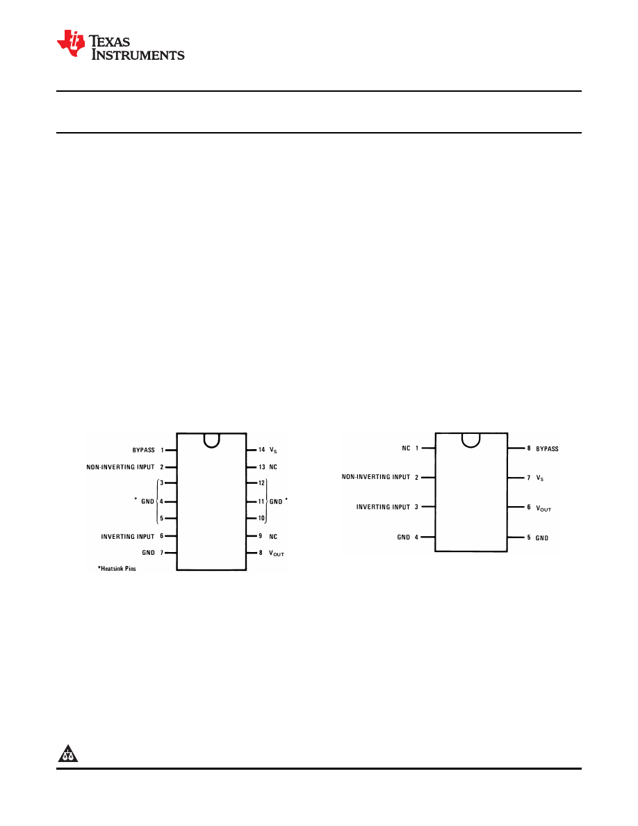
Connection Diagrams
(Dual-In-Line Packages, Top View)
Figure 1. 14-Pin PDIP
Figure 2. 8-Pin PDIP
See NFF0014A Package
See P Package
1
Please be aware that an important notice concerning availability, standard warranty, and use in critical applications of
Texas Instruments semiconductor products and disclaimers thereto appears at the end of this data sheet.
PRODUCTION DATA information is current as of publication date.
Copyright © 1994-2013, Texas Instruments Incorporated
Products conform to specifications per the terms of the Texas
Instruments standard warranty. Production processing does not
necessarily include testing of all parameters.
SNAS546C - DECEMBER 1994 - REVISED APRIL 2013
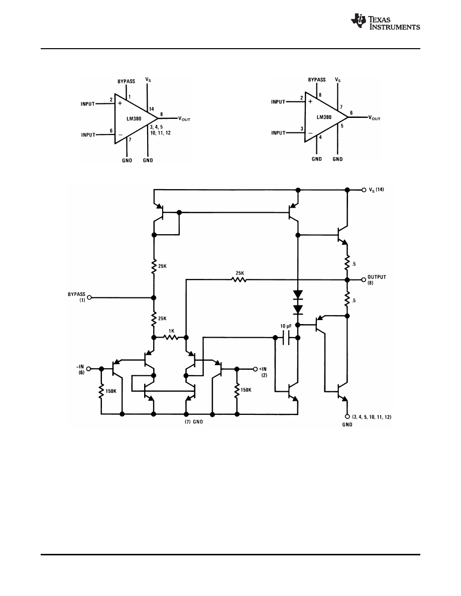
Block and Schematic Diagrams
Figure 3. 14-Pin PDIP
Figure 4. 8-Pin PDIP
Figure 5.
2
Copyright © 1994-2013, Texas Instruments Incorporated
Product Folder Links:
SNAS546C - DECEMBER 1994 - REVISED APRIL 2013
These devices have limited built-in ESD protection. The leads should be shorted together or the device placed in conductive foam
during storage or handling to prevent electrostatic damage to the MOS gates.
Absolute Maximum Ratings
(1) (2)
Supply Voltage
22V
Peak Current
1.3A
Package Dissipation
14-Pin PDIP
(3)
8.3W
8-Pin PDIP
(3)
1.67W
Input Voltage
±0.5V
Storage Temperature
-
65 °C to +150 °C
Operating Temperature
0 °C to +70 °C
Junction Temperature
+150 °C
Lead Temperature (Soldering, 10 sec.)
+260 °C
ESD rating to be determined
Thermal Resistance
Θ
JC
(14-Pin PDIP)
30 °C/W
Θ
JC
(8-Pin PDIP)
37 °C/W
Θ
JA
(14-Pin PDIP)
79 °C/W
Θ
JA
(8-Pin PDIP)
107 °C/W
(1)
"Absolute Maximum Ratings" indicate limits beyond which damage to the device may occur. Operating Ratings indicate conditions for
which the device is functional, but do not ensure specific performance limits.
(2)
If Military/Aerospace specified devices are required, please contact the Texas Instruments Sales Office/Distributors for availability and
specifications.
(3)
The package is to be derated at 15 °C/W junction to heat sink pins for 14-pin pkg; 75 °C/W for 8-pin.
Electrical Characteristics
(1)
Symbol
Parameter
Conditions
Min
Typ
Max
Units
P
OUT(RMS)
Output Power
R
L
= 8
Ω
, THD = 3%
(2) (3)
2.5
W
A
V
Gain
40
50
60
V/V
V
OUT
Output Voltage Swing
R
L
= 8
Ω
14
V
p-p
Z
IN
Input Resistance
150k
Ω
THD
Total Harmonic Distortion
See
(3) (4)
0.2
%
PSRR
Power Supply Rejection Ratio
See
(5)
38
dB
V
S
Supply Voltage
10
22
V
BW
Bandwidth
P
OUT
= 2W, R
L
= 8
Ω
100k
Hz
I
Q
Quiescent Supply Current
7
25
mA
V
OUTQ
Quiescent Output Voltage
8
9.0
10
V
I
BIAS
Bias Current
Inputs Floating
100
nA
I
SC
Short Circuit Current
1.3
A
(1)
V
S
= 18V and T
A
= 25 °C unless otherwise specified.
(2)
With device Pins 3, 4, 5, 10, 11, 12 soldered into a 1/16
³
epoxy glass board with 2 ounce copper foil with a minimum surface of 6 square
inches.
(3)
C
BYPASS
= 0.47
μ
fd on Pin 1.
(4)
The maximum junction temperature of the LM380 is 150 °C.
(5)
Rejection ratio referred to the output with C
BYPASS
= 5
μ
F.
Copyright © 1994-2013, Texas Instruments Incorporated
3
Product Folder Links:
SNAS546C - DECEMBER 1994 - REVISED APRIL 2013
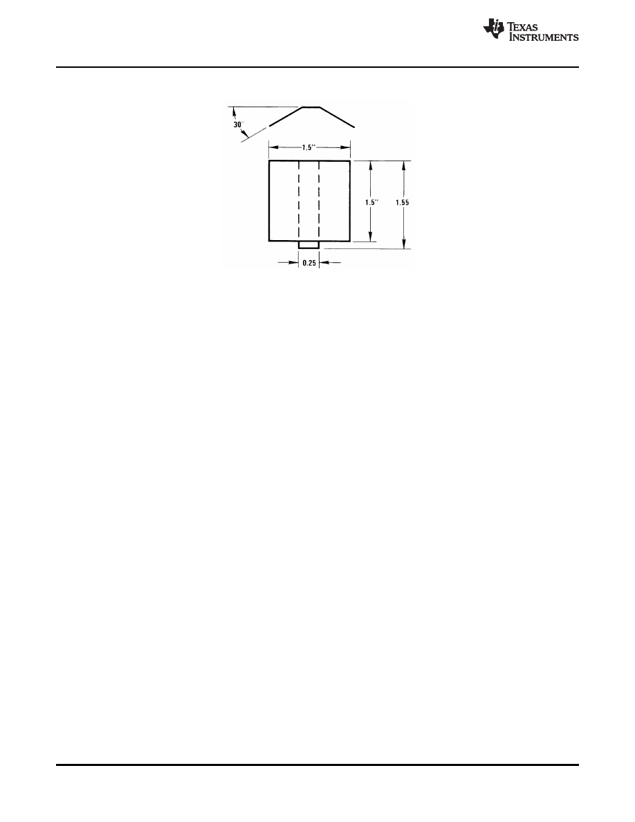
Heat Sink Dimensions
Staver Heat Sink #V-7
Staver Company
41 Saxon Ave.
P.O. Drawer H
Bayshore, NY 11706
Tel: (516) 666-8000
Copper Wings
2 Required
Soldered to
Pins 3, 4, 5,
10, 11, 12
Thickness 0.04
Inches
4
Copyright © 1994-2013, Texas Instruments Incorporated
Product Folder Links:
SNAS546C - DECEMBER 1994 - REVISED APRIL 2013
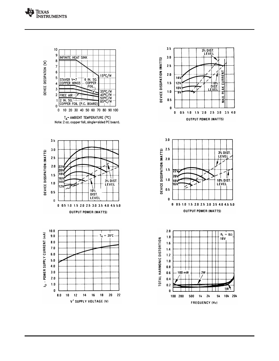
Typical Performance Characteristics
Maximum Device Dissipation vs Ambient Temperature
Device Dissipation vs Output Power4
Ω
Load
Figure 6.
Figure 7.
Device Dissipation vs Output Power8
Ω
Load
Device Dissipation vsOutput Power16
Ω
Load
Figure 8.
Figure 9.
Power Supply Current vs Supply Voltage
Total Harmonic Distortion vs Frequency
Figure 10.
Figure 11.
Copyright © 1994-2013, Texas Instruments Incorporated
5
Product Folder Links:

SNAS546C - DECEMBER 1994 - REVISED APRIL 2013
Typical Performance Characteristics (continued)
Output Voltage Gain and Phase vs Frequency
Total Harmonic Distortion vs Output Power
Figure 12.
Figure 13.
Device Dissipation vs Output Power
Supply Decoupling vs Frequency
Figure 14.
Figure 15.
6
Copyright © 1994-2013, Texas Instruments Incorporated
Product Folder Links:
SNAS546C - DECEMBER 1994 - REVISED APRIL 2013
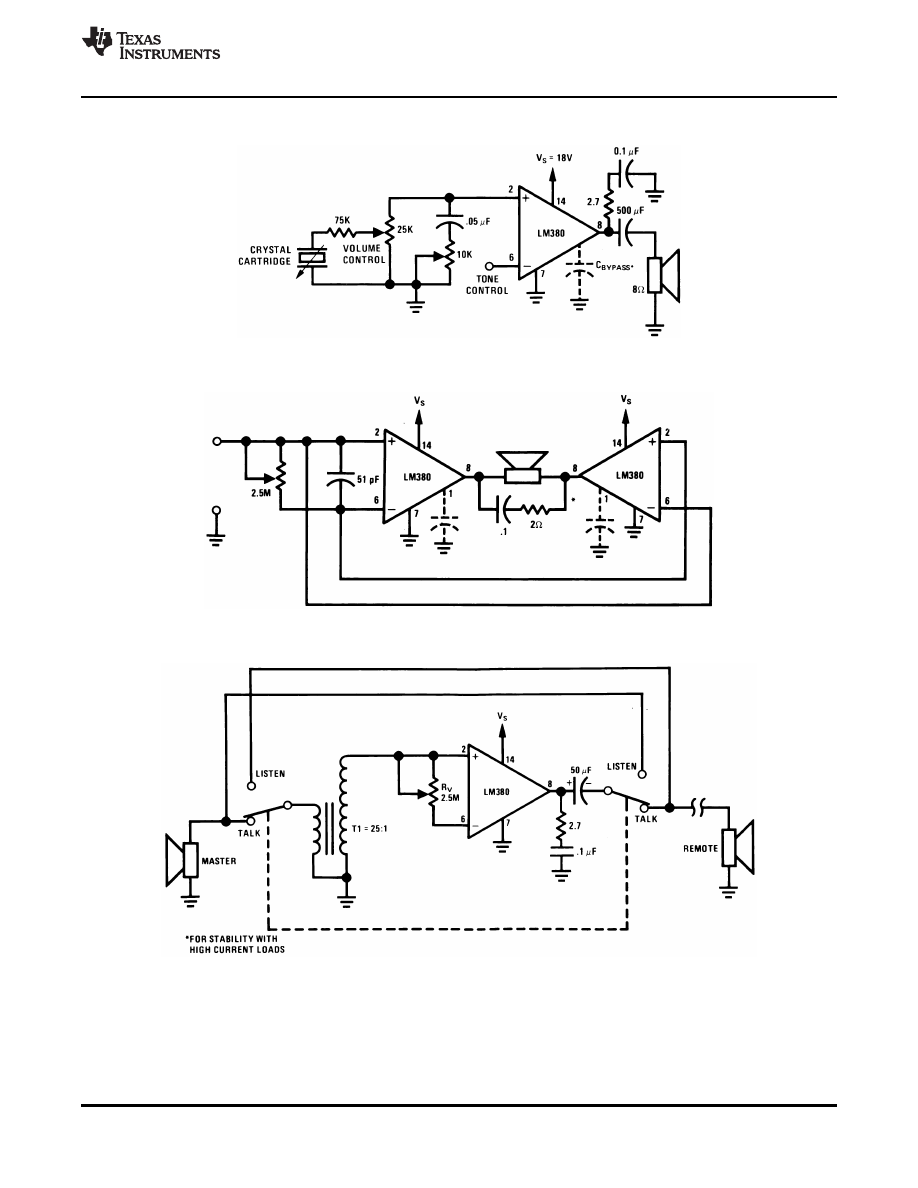
Typical Applications
Figure 16. Phono Amplifier
Figure 17. Bridge Amplifier
Figure 18. Intercom
Copyright © 1994-2013, Texas Instruments Incorporated
7
Product Folder Links:
SNAS546C - DECEMBER 1994 - REVISED APRIL 2013
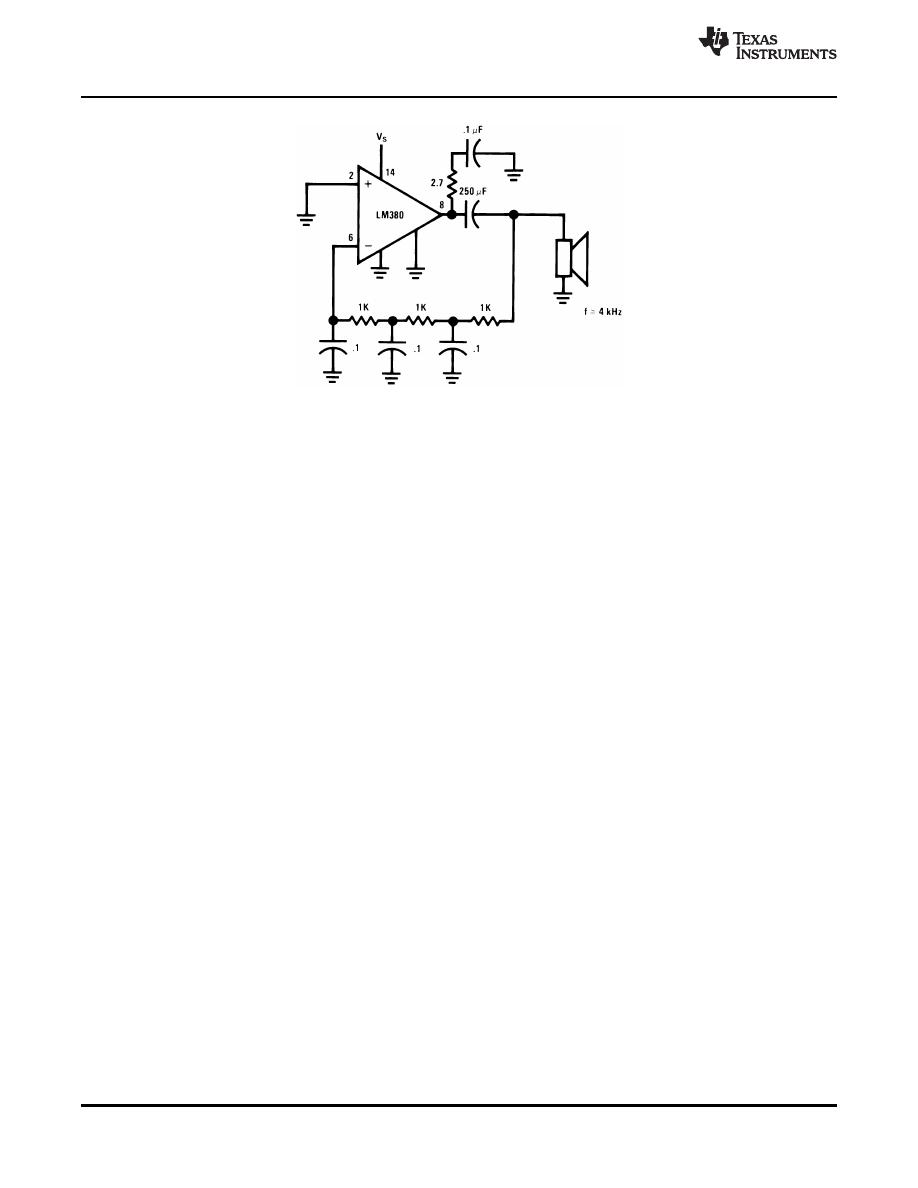
Figure 19. Phase Shift Oscillator
8
Copyright © 1994-2013, Texas Instruments Incorporated
Product Folder Links:
SNAS546C - DECEMBER 1994 - REVISED APRIL 2013
REVISION HISTORY
Changes from Revision B (April 2013) to Revision C
Page
Changed layout of National Data Sheet to TI format ............................................................................................................
Copyright © 1994-2013, Texas Instruments Incorporated
9
Product Folder Links:
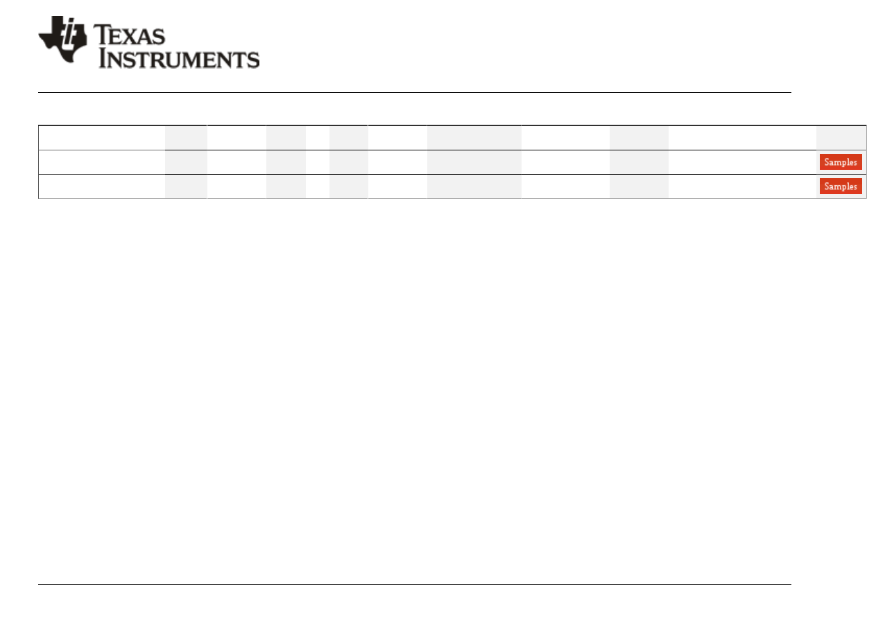
PACKAGE OPTION ADDENDUM
www.ti.com
30-Jun-2016
Addendum-Page 1
PACKAGING INFORMATION
Orderable Device
Status
(1)
Package Type Package
Drawing
Pins Package
Qty
Eco Plan
(2)
Lead/Ball Finish
(6)
MSL Peak Temp
(3)
Op Temp ( °C)
Device Marking
(4/5)
Samples
LM380N-8/NOPB
ACTIVE
PDIP
P
8
40
Green (RoHS
& no Sb/Br)
CU SN
Level-1-NA-UNLIM
0 to 70
LM
380N-8
LM380N/NOPB
ACTIVE
PDIP
NFF
14
25
Green (RoHS
& no Sb/Br)
CU SN
Level-1-NA-UNLIM
0 to 70
LM380N
(1)
The marketing status values are defined as follows:
ACTIVE: Product device recommended for new designs.
LIFEBUY: TI has announced that the device will be discontinued, and a lifetime-buy period is in effect.
NRND: Not recommended for new designs. Device is in production to support existing customers, but TI does not recommend using this part in a new design.
PREVIEW: Device has been announced but is not in production. Samples may or may not be available.
OBSOLETE: TI has discontinued the production of the device.
(2)
Eco Plan - The planned eco-friendly classification: Pb-Free (RoHS), Pb-Free (RoHS Exempt), or Green (RoHS & no Sb/Br) - please check
for the latest availability
information and additional product content details.
TBD: The Pb-Free/Green conversion plan has not been defined.
Pb-Free (RoHS): TI's terms "Lead-Free" or "Pb-Free" mean semiconductor products that are compatible with the current RoHS requirements for all 6 substances, including the requirement that
lead not exceed 0.1% by weight in homogeneous materials. Where designed to be soldered at high temperatures, TI Pb-Free products are suitable for use in specified lead-free processes.
Pb-Free (RoHS Exempt): This component has a RoHS exemption for either 1) lead-based flip-chip solder bumps used between the die and package, or 2) lead-based die adhesive used between
the die and leadframe. The component is otherwise considered Pb-Free (RoHS compatible) as defined above.
Green (RoHS & no Sb/Br): TI defines "Green" to mean Pb-Free (RoHS compatible), and free of Bromine (Br) and Antimony (Sb) based flame retardants (Br or Sb do not exceed 0.1% by weight
in homogeneous material)
(3)
MSL, Peak Temp. - The Moisture Sensitivity Level rating according to the JEDEC industry standard classifications, and peak solder temperature.
(4)
There may be additional marking, which relates to the logo, the lot trace code information, or the environmental category on the device.
(5)
Multiple Device Markings will be inside parentheses. Only one Device Marking contained in parentheses and separated by a "~" will appear on a device. If a line is indented then it is a continuation
of the previous line and the two combined represent the entire Device Marking for that device.
(6)
Lead/Ball Finish - Orderable Devices may have multiple material finish options. Finish options are separated by a vertical ruled line. Lead/Ball Finish values may wrap to two lines if the finish
value exceeds the maximum column width.
Important Information and Disclaimer:The information provided on this page represents TI's knowledge and belief as of the date that it is provided. TI bases its knowledge and belief on information
provided by third parties, and makes no representation or warranty as to the accuracy of such information. Efforts are underway to better integrate information from third parties. TI has taken and
continues to take reasonable steps to provide representative and accurate information but may not have conducted destructive testing or chemical analysis on incoming materials and chemicals.
TI and TI suppliers consider certain information to be proprietary, and thus CAS numbers and other limited information may not be available for release.
PACKAGE OPTION ADDENDUM
www.ti.com
30-Jun-2016
Addendum-Page 2
In no event shall TI's liability arising out of such information exceed the total purchase price of the TI part(s) at issue in this document sold by TI to Customer on an annual basis.
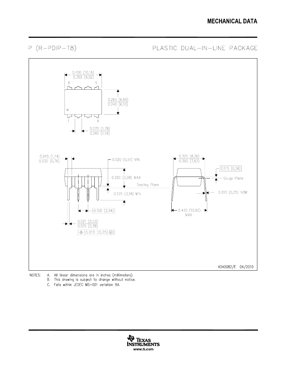
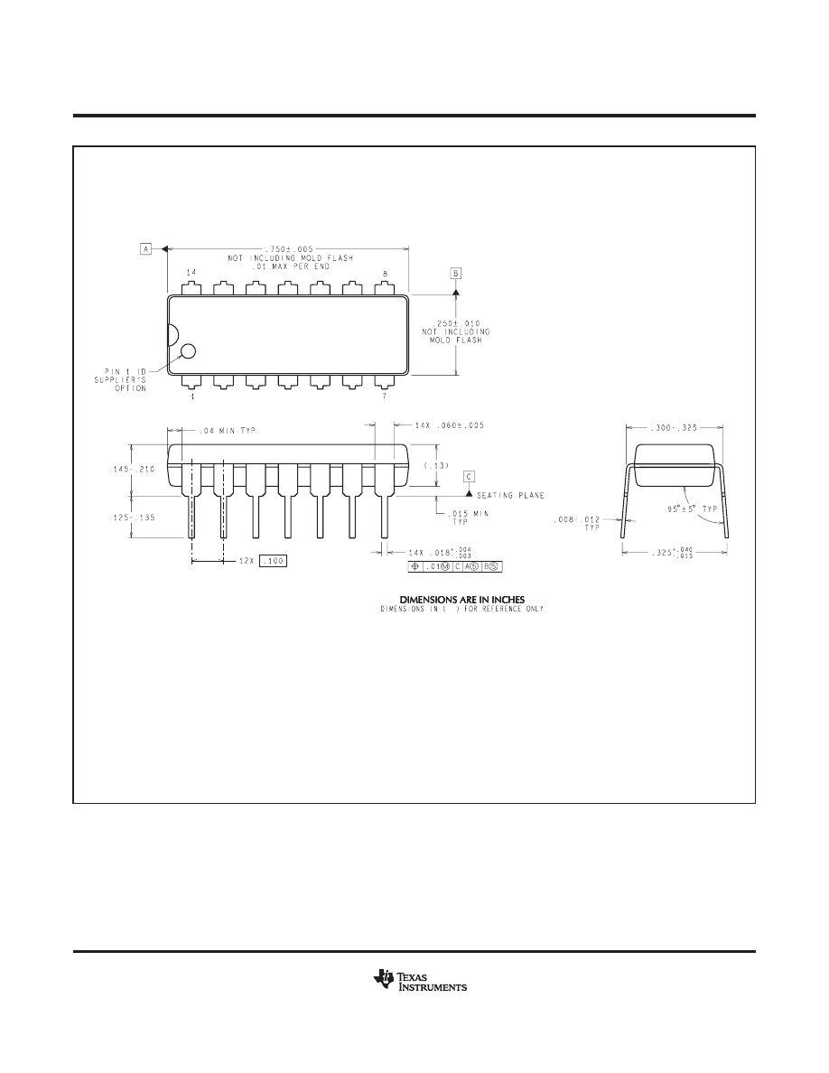
MECHANICAL DATA
N0014A
www.ti.com
N14A (Rev G)
NFF0014A

IMPORTANT NOTICE
Texas Instruments Incorporated and its subsidiaries (TI) reserve the right to make corrections, enhancements, improvements and other
changes to its semiconductor products and services per JESD46, latest issue, and to discontinue any product or service per JESD48, latest
issue. Buyers should obtain the latest relevant information before placing orders and should verify that such information is current and
complete. All semiconductor products (also referred to herein as components) are sold subject to TIs terms and conditions of sale
supplied at the time of order acknowledgment.
TI warrants performance of its components to the specifications applicable at the time of sale, in accordance with the warranty in TIs terms
and conditions of sale of semiconductor products. Testing and other quality control techniques are used to the extent TI deems necessary
to support this warranty. Except where mandated by applicable law, testing of all parameters of each component is not necessarily
performed.
TI assumes no liability for applications assistance or the design of Buyers products. Buyers are responsible for their products and
applications using TI components. To minimize the risks associated with Buyers products and applications, Buyers should provide
adequate design and operating safeguards.
TI does not warrant or represent that any license, either express or implied, is granted under any patent right, copyright, mask work right, or
other intellectual property right relating to any combination, machine, or process in which TI components or services are used. Information
published by TI regarding third-party products or services does not constitute a license to use such products or services or a warranty or
endorsement thereof. Use of such information may require a license from a third party under the patents or other intellectual property of the
third party, or a license from TI under the patents or other intellectual property of TI.
Reproduction of significant portions of TI information in TI data books or data sheets is permissible only if reproduction is without alteration
and is accompanied by all associated warranties, conditions, limitations, and notices. TI is not responsible or liable for such altered
documentation. Information of third parties may be subject to additional restrictions.
Resale of TI components or services with statements different from or beyond the parameters stated by TI for that component or service
voids all express and any implied warranties for the associated TI component or service and is an unfair and deceptive business practice.
TI is not responsible or liable for any such statements.
Buyer acknowledges and agrees that it is solely responsible for compliance with all legal, regulatory and safety-related requirements
concerning its products, and any use of TI components in its applications, notwithstanding any applications-related information or support
that may be provided by TI. Buyer represents and agrees that it has all the necessary expertise to create and implement safeguards which
anticipate dangerous consequences of failures, monitor failures and their consequences, lessen the likelihood of failures that might cause
harm and take appropriate remedial actions. Buyer will fully indemnify TI and its representatives against any damages arising out of the use
of any TI components in safety-critical applications.
In some cases, TI components may be promoted specifically to facilitate safety-related applications. With such components, TIs goal is to
help enable customers to design and create their own end-product solutions that meet applicable functional safety standards and
requirements. Nonetheless, such components are subject to these terms.
No TI components are authorized for use in FDA Class III (or similar life-critical medical equipment) unless authorized officers of the parties
have executed a special agreement specifically governing such use.
Only those TI components which TI has specifically designated as military grade or enhanced plastic are designed and intended for use in
military/aerospace applications or environments. Buyer acknowledges and agrees that any military or aerospace use of TI components
which have not been so designated is solely at the Buyer's risk, and that Buyer is solely responsible for compliance with all legal and
regulatory requirements in connection with such use.
TI has specifically designated certain components as meeting ISO/TS16949 requirements, mainly for automotive use. In any case of use of
non-designated products, TI will not be responsible for any failure to meet ISO/TS16949.
Products
Applications
Audio
Automotive and Transportation
Amplifiers
Communications and Telecom
Data Converters
Computers and Peripherals
DLP ® Products
Consumer Electronics
DSP
Energy and Lighting
Clocks and Timers
Industrial
Interface
Medical
Logic
Security
Power Mgmt
Space, Avionics and Defense
Microcontrollers
Video and Imaging
RFID
OMAP Applications Processors
TI E2E Community
Wireless Connectivity
Mailing Address: Texas Instruments, Post Office Box 655303, Dallas, Texas 75265
Copyright © 2016, Texas Instruments Incorporated
Document Outline

