| Secciones |
|---|
| Foros Electrónica |
|
|
| Boletines de correo |
 |

LM386
LM386 Low Voltage Audio Power Amplifier
Literature Number: SNAS545A
LM386
Low Voltage Audio Power Amplifier
General Description
The LM386 is a power amplifier designed for use in low volt-
age consumer applications. The gain is internally set to 20 to
keep external part count low, but the addition of an external
resistor and capacitor between pins 1 and 8 will increase the
gain to any value from 20 to 200.
The inputs are ground referenced while the output automati-
cally biases to one-half the supply voltage. The quiescent
power drain is only 24 milliwatts when operating from a 6 volt
supply, making the LM386 ideal for battery operation.
Features
n
Battery operation
n
Minimum external parts
n
Wide supply voltage range: 4V-12V or 5V-18V
n
Low quiescent current drain: 4mA
n
Voltage gains from 20 to 200
n
Ground referenced input
n
Self-centering output quiescent voltage
n
Low distortion: 0.2% (A
V
= 20, V
S
= 6V, R
L
= 8
Ω¦
, P
O
=
125mW, f = 1kHz)
n
Available in 8 pin MSOP package
Applications
n
AM-FM radio amplifiers
n
Portable tape player amplifiers
n
Intercoms
n
TV sound systems
n
Line drivers
n
Ultrasonic drivers
n
Small servo drivers
n
Power converters
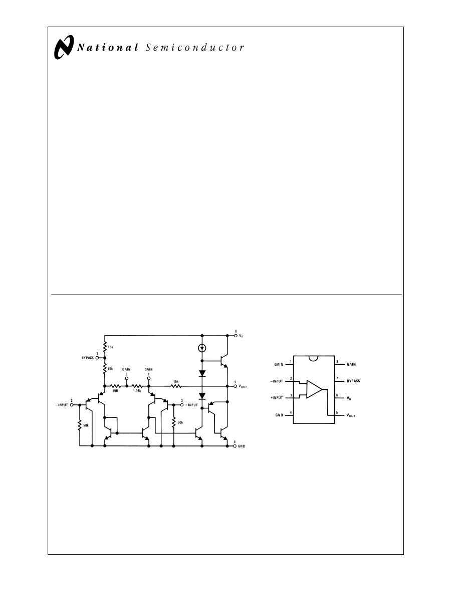
Equivalent Schematic and Connection Diagrams
DS006976-1
Small Outline,
Molded Mini Small Outline,
and Dual-In-Line Packages
DS006976-2
Top View
Order Number LM386M-1,
LM386MM-1, LM386N-1,
LM386N-3 or LM386N-4
See NS Package Number
M08A, MUA08A or N08E
August 2000
LM386
Low
V
oltage
Audio
Power
Amplifier
© 2000 National Semiconductor Corporation
DS006976
www.national.com
Absolute Maximum Ratings
(Note 2)
If Military/Aerospace specified devices are required,
please contact the National Semiconductor Sales Office/
Distributors for availability and specifications.
Supply Voltage
(LM386N-1, -3, LM386M-1)
15V
Supply Voltage (LM386N-4)
22V
Package Dissipation (Note 3)
(LM386N)
1.25W
(LM386M)
0.73W
(LM386MM-1)
0.595W
Input Voltage
±
0.4V
Storage Temperature
-65°C to +150°C
Operating Temperature
0°C to +70°C
Junction Temperature
+150°C
Soldering Information
Dual-In-Line Package
Soldering (10 sec)
+260°C
Small Outline Package
(SOIC and MSOP)
Vapor Phase (60 sec)
+215°C
Infrared (15 sec)
+220°C
See AN-450 Surface Mounting Methods and Their Effect
on Product Reliability for other methods of soldering
surface mount devices.
Thermal Resistance
Θ
JC
(DIP)
37°C/W
Θ
JA
(DIP)
107°C/W
Θ
JC
(SO Package)
35°C/W
Θ
JA
(SO Package)
172°C/W
Θ
JA
(MSOP)
210°C/W
Θ
JC
(MSOP)
56°C/W
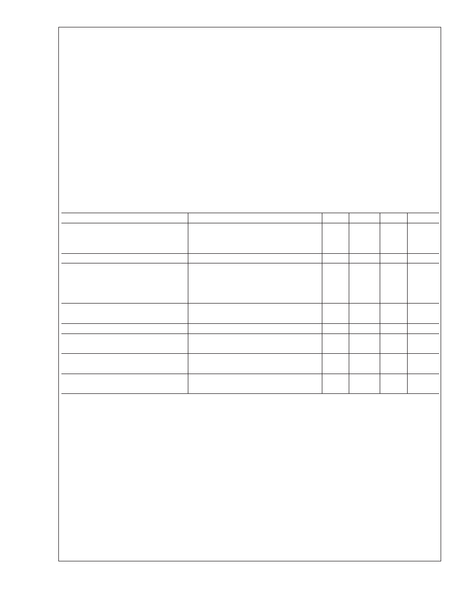
Electrical Characteristics
(Notes 1, 2)
T
A
= 25°C
Parameter
Conditions
Min
Typ
Max
Units
Operating Supply Voltage (V
S
)
LM386N-1, -3, LM386M-1, LM386MM-1
4
12
V
LM386N-4
5
18
V
Quiescent Current (I
Q
)
V
S
= 6V, V
IN
= 0
4
8
mA
Output Power (P
OUT
)
LM386N-1, LM386M-1, LM386MM-1
V
S
= 6V, R
L
= 8
Ω¦
, THD = 10%
250
325
mW
LM386N-3
V
S
= 9V, R
L
= 8
Ω¦
, THD = 10%
500
700
mW
LM386N-4
V
S
= 16V, R
L
= 32
Ω¦
, THD = 10%
700
1000
mW
Voltage Gain (A
V
)
V
S
= 6V, f = 1 kHz
26
dB
10 µF from Pin 1 to 8
46
dB
Bandwidth (BW)
V
S
= 6V, Pins 1 and 8 Open
300
kHz
Total Harmonic Distortion (THD)
V
S
= 6V, R
L
= 8
Ω¦
, P
OUT
= 125 mW
0.2
%
f = 1 kHz, Pins 1 and 8 Open
Power Supply Rejection Ratio (PSRR)
V
S
= 6V, f = 1 kHz, C
BYPASS
= 10 µF
50
dB
Pins 1 and 8 Open, Referred to Output
Input Resistance (R
IN
)
50
k
Ω¦
Input Bias Current (I
BIAS
)
V
S
= 6V, Pins 2 and 3 Open
250
nA
Note 1: All voltages are measured with respect to the ground pin, unless otherwise specified.
Note 2: Absolute Maximum Ratings indicate limits beyond which damage to the device may occur. Operating Ratings indicate conditions for which the device is func-
tional, but do not guarantee specific performance limits. Electrical Characteristics state DC and AC electrical specifications under particular test conditions which guar-
antee specific performance limits. This assumes that the device is within the Operating Ratings. Specifications are not guaranteed for parameters where no limit is
given, however, the typical value is a good indication of device performance.
Note 3: For operation in ambient temperatures above 25°C, the device must be derated based on a 150°C maximum junction temperature and 1) a thermal resis-
tance of 107°C/W junction to ambient for the dual-in-line package and 2) a thermal resistance of 170°C/W for the small outline package.
LM386
www.national.com
2

Application Hints
GAIN CONTROL
To make the LM386 a more versatile amplifier, two pins (1
and 8) are provided for gain control. With pins 1 and 8 open
the 1.35 k
Ω¦
resistor sets the gain at 20 (26 dB). If a capacitor
is put from pin 1 to 8, bypassing the 1.35 k
Ω¦
resistor, the
gain will go up to 200 (46 dB). If a resistor is placed in series
with the capacitor, the gain can be set to any value from 20
to 200. Gain control can also be done by capacitively cou-
pling a resistor (or FET) from pin 1 to ground.
Additional external components can be placed in parallel
with the internal feedback resistors to tailor the gain and fre-
quency response for individual applications. For example,
we can compensate poor speaker bass response by fre-
quency shaping the feedback path. This is done with a series
RC from pin 1 to 5 (paralleling the internal 15 k
Ω¦
resistor).
For 6 dB effective bass boost: R
.
15 k
Ω¦
, the lowest value
for good stable operation is R = 10 k
Ω¦
if pin 8 is open. If pins
1 and 8 are bypassed then R as low as 2 k
Ω¦
can be used.
This restriction is because the amplifier is only compensated
for closed-loop gains greater than 9.
INPUT BIASING
The schematic shows that both inputs are biased to ground
with a 50 k
Ω¦
resistor. The base current of the input transis-
tors is about 250 nA, so the inputs are at about 12.5 mV
when left open. If the dc source resistance driving the LM386
is higher than 250 k
Ω¦
it will contribute very little additional
offset (about 2.5 mV at the input, 50 mV at the output). If the
dc source resistance is less than 10 k
Ω¦
, then shorting the
unused input to ground will keep the offset low (about 2.5 mV
at the input, 50 mV at the output). For dc source resistances
between these values we can eliminate excess offset by put-
ting a resistor from the unused input to ground, equal in
value to the dc source resistance. Of course all offset prob-
lems are eliminated if the input is capacitively coupled.
When using the LM386 with higher gains (bypassing the
1.35 k
Ω¦
resistor between pins 1 and 8) it is necessary to by-
pass the unused input, preventing degradation of gain and
possible instabilities. This is done with a 0.1 µF capacitor or
a short to ground depending on the dc source resistance on
the driven input.
LM386
www.national.com
3
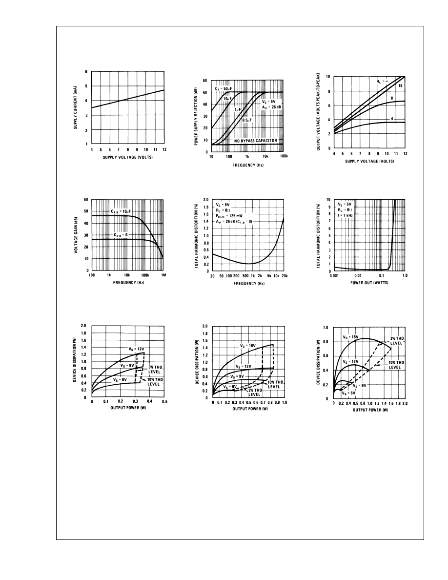
Typical Performance Characteristics
Quiescent Supply Current
vs Supply Voltage
DS006976-5
Power Supply Rejection Ratio
(Referred to the Output)
vs Frequency
DS006976-12
Peak-to-Peak Output Voltage
Swing vs Supply Voltage
DS006976-13
Voltage Gain vs Frequency
DS006976-14
Distortion vs Frequency
DS006976-15
Distortion vs Output Power
DS006976-16
Device Dissipation vs Output
Power 4
Ω¦
Load
DS006976-17
Device Dissipation vs Output
Power 8
Ω¦
Load
DS006976-18
Device Dissipation vs Output
Power 16
Ω¦
Load
DS006976-19
LM386
www.national.com
4
Typical Applications
Amplifier with Gain = 20
Minimum Parts
DS006976-3
Amplifier with Gain = 200
DS006976-4
Amplifier with Gain = 50
DS006976-6
Low Distortion Power Wienbridge Oscillator
DS006976-7
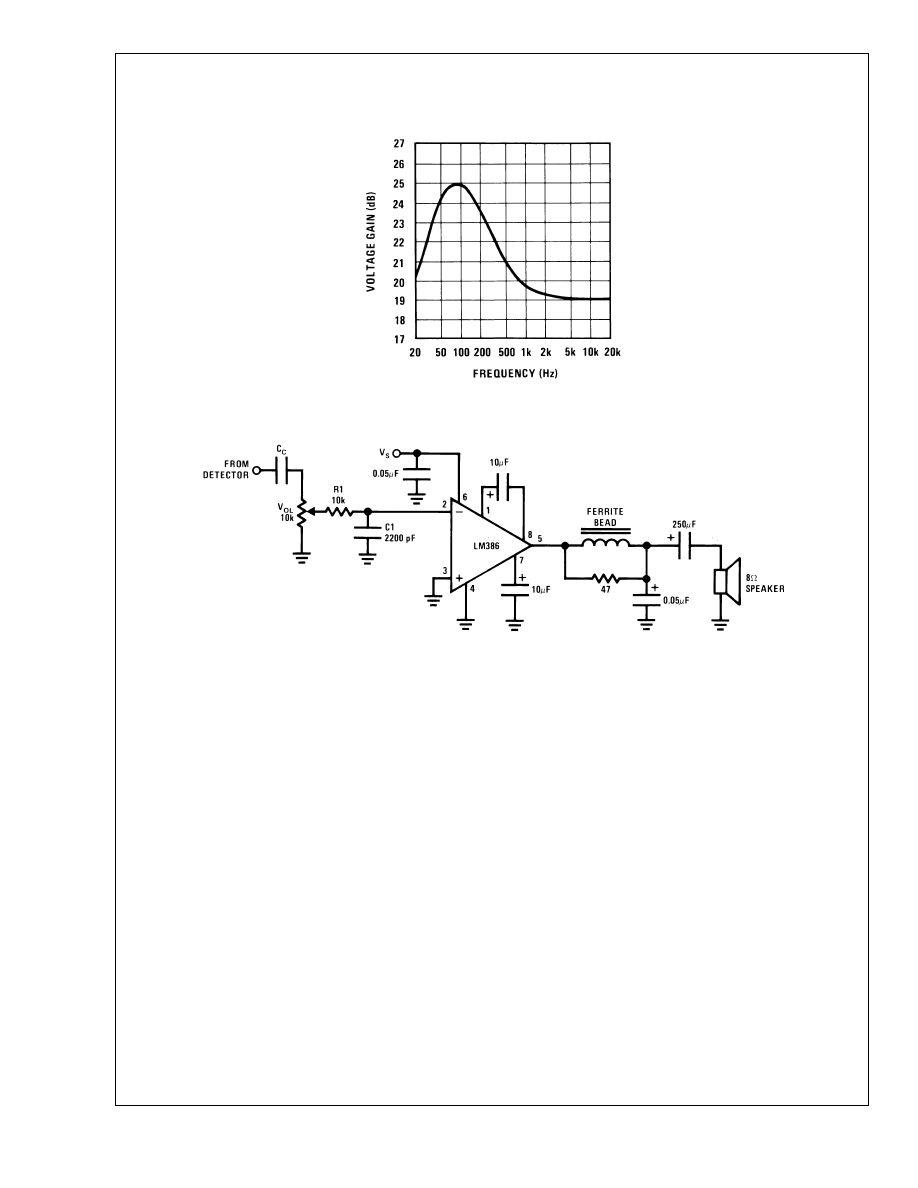
Amplifier with Bass Boost
DS006976-8
Square Wave Oscillator
DS006976-9
LM386
www.national.com
5
Typical Applications
(Continued)
Note 4: Twist Supply lead and supply ground very tightly.
Note 5: Twist speaker lead and ground very tightly.
Note 6: Ferrite bead in Ferroxcube K5-001-001/3B with 3 turns of wire.
Note 7: R1C1 band limits input signals.
Note 8: All components must be spaced very closely to IC.
Frequency Response with Bass Boost
DS006976-10
AM Radio Power Amplifier
DS006976-11
LM386
www.national.com
6
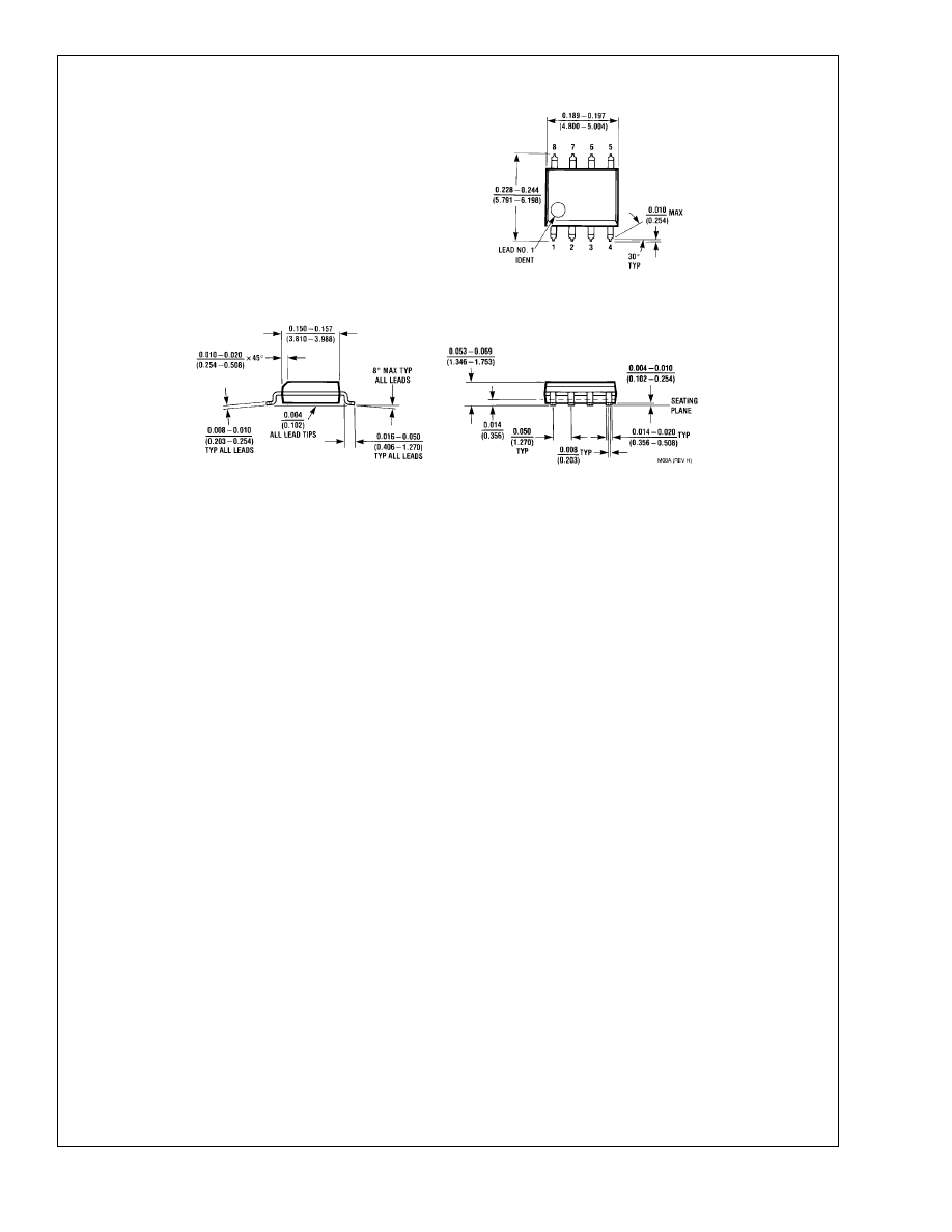
Physical Dimensions
inches (millimeters) unless otherwise noted
SO Package (M)
Order Number LM386M-1
NS Package Number M08A
LM386
www.national.com
7
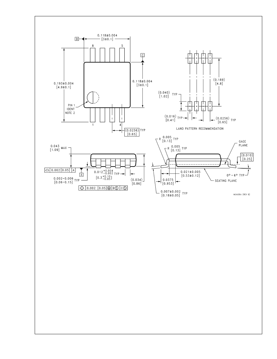
Physical Dimensions
inches (millimeters) unless otherwise noted (Continued)
8-Lead (0.118 Wide) Molded Mini Small Outline Package
Order Number LM386MM-1
NS Package Number MUA08A
LM386
www.national.com
8
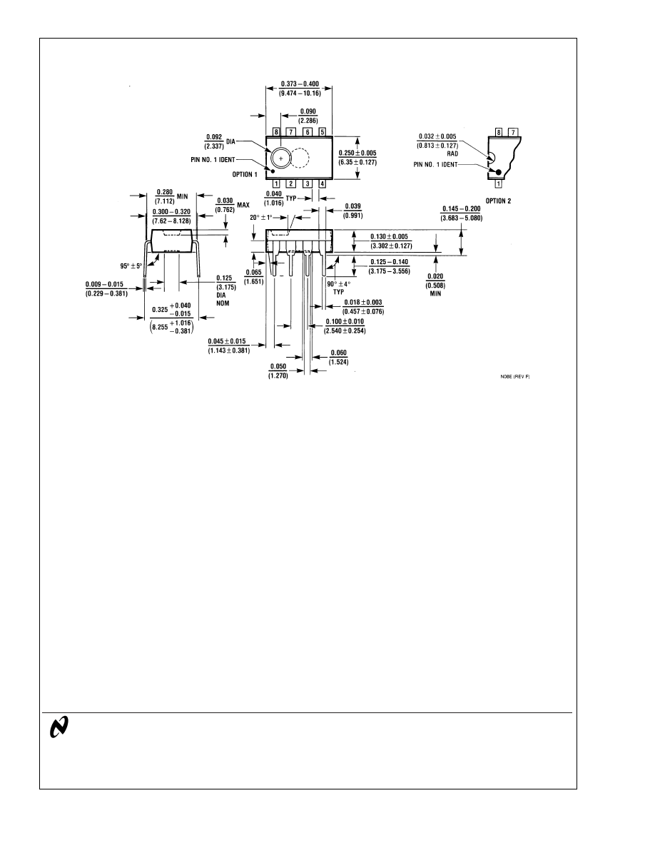
Physical Dimensions
inches (millimeters) unless otherwise noted (Continued)
LIFE SUPPORT POLICY
NATIONALS PRODUCTS ARE NOT AUTHORIZED FOR USE AS CRITICAL COMPONENTS IN LIFE SUPPORT
DEVICES OR SYSTEMS WITHOUT THE EXPRESS WRITTEN APPROVAL OF THE PRESIDENT AND GENERAL
COUNSEL OF NATIONAL SEMICONDUCTOR CORPORATION. As used herein:
1. Life support devices or systems are devices or
systems which, (a) are intended for surgical implant
into the body, or (b) support or sustain life, and
whose failure to perform when properly used in
accordance with instructions for use provided in the
labeling, can be reasonably expected to result in a
significant injury to the user.
2. A critical component is any component of a life
support device or system whose failure to perform
can be reasonably expected to cause the failure of
the life support device or system, or to affect its
safety or effectiveness.
National Semiconductor
Corporation
Americas
Tel: 1-800-272-9959
Fax: 1-800-737-7018
Email: support@nsc.com
National Semiconductor
Europe
Fax: +49 (0) 180-530 85 86
Email: europe.support@nsc.com
Deutsch Tel: +49 (0) 69 9508 6208
English
Tel: +44 (0) 870 24 0 2171
Français Tel: +33 (0) 1 41 91 8790
National Semiconductor
Asia Pacific Customer
Response Group
Tel: 65-2544466
Fax: 65-2504466
Email: ap.support@nsc.com
National Semiconductor
Japan Ltd.
Tel: 81-3-5639-7560
Fax: 81-3-5639-7507
www.national.com
Dual-In-Line Package (N)
Order Number LM386N-1, LM386N-3 or LM386N-4
NS Package Number N08E
LM386
Low
V
oltage
Audio
Power
Amplifier
National does not assume any responsibility for use of any circuitry described, no circuit patent licenses are implied and National reserves the right at any time without notice to change said circuitry and specifications.

IMPORTANT NOTICE
Texas Instruments Incorporated and its subsidiaries (TI) reserve the right to make corrections, modifications, enhancements, improvements,
and other changes to its products and services at any time and to discontinue any product or service without notice. Customers should
obtain the latest relevant information before placing orders and should verify that such information is current and complete. All products are
sold subject to TI
s terms and conditions of sale supplied at the time of order acknowledgment.
TI warrants performance of its hardware products to the specifications applicable at the time of sale in accordance with TI
s standard
warranty. Testing and other quality control techniques are used to the extent TI deems necessary to support this warranty. Except where
mandated by government requirements, testing of all parameters of each product is not necessarily performed.
TI assumes no liability for applications assistance or customer product design. Customers are responsible for their products and
applications using TI components. To minimize the risks associated with customer products and applications, customers should provide
adequate design and operating safeguards.
TI does not warrant or represent that any license, either express or implied, is granted under any TI patent right, copyright, mask work right,
or other TI intellectual property right relating to any combination, machine, or process in which TI products or services are used. Information
published by TI regarding third-party products or services does not constitute a license from TI to use such products or services or a
warranty or endorsement thereof. Use of such information may require a license from a third party under the patents or other intellectual
property of the third party, or a license from TI under the patents or other intellectual property of TI.
Reproduction of TI information in TI data books or data sheets is permissible only if reproduction is without alteration and is accompanied
by all associated warranties, conditions, limitations, and notices. Reproduction of this information with alteration is an unfair and deceptive
business practice. TI is not responsible or liable for such altered documentation. Information of third parties may be subject to additional
restrictions.
Resale of TI products or services with statements different from or beyond the parameters stated by TI for that product or service voids all
express and any implied warranties for the associated TI product or service and is an unfair and deceptive business practice. TI is not
responsible or liable for any such statements.
TI products are not authorized for use in safety-critical applications (such as life support) where a failure of the TI product would reasonably
be expected to cause severe personal injury or death, unless officers of the parties have executed an agreement specifically governing
such use. Buyers represent that they have all necessary expertise in the safety and regulatory ramifications of their applications, and
acknowledge and agree that they are solely responsible for all legal, regulatory and safety-related requirements concerning their products
and any use of TI products in such safety-critical applications, notwithstanding any applications-related information or support that may be
provided by TI. Further, Buyers must fully indemnify TI and its representatives against any damages arising out of the use of TI products in
such safety-critical applications.
TI products are neither designed nor intended for use in military/aerospace applications or environments unless the TI products are
specifically designated by TI as military-grade or
"
enhanced plastic.
"
Only products designated by TI as military-grade meet military
specifications. Buyers acknowledge and agree that any such use of TI products which TI has not designated as military-grade is solely at
the Buyer
'
s risk, and that they are solely responsible for compliance with all legal and regulatory requirements in connection with such use.
TI products are neither designed nor intended for use in automotive applications or environments unless the specific TI products are
designated by TI as compliant with ISO/TS 16949 requirements. Buyers acknowledge and agree that, if they use any non-designated
products in automotive applications, TI will not be responsible for any failure to meet such requirements.
Following are URLs where you can obtain information on other Texas Instruments products and application solutions:
Products
Applications
Audio
Communications and Telecom
Amplifiers
Computers and Peripherals
Data Converters
Consumer Electronics
DLP
®
Products
Energy and Lighting
DSP
Industrial
Clocks and Timers
Medical
Interface
Security
Logic
Space, Avionics and Defense
Power Mgmt
Transportation and Automotive
Microcontrollers
Video and Imaging
RFID
OMAP Mobile Processors
Wireless Connectivity
TI E2E Community Home Page
Mailing Address: Texas Instruments, Post Office Box 655303, Dallas, Texas 75265
Copyright
©
2011, Texas Instruments Incorporated

