| Secciones |
|---|
| Foros Electrónica |
|
|
| Boletines de correo |
 |
SNAS548D - FEBRUARY 2000 - REVISED JANUARY 2015
LM555 Timer
1 Features
3 Description
The LM555 is a highly stable device for generating
1
Direct Replacement for SE555/NE555
accurate
time
delays
or
oscillation.
Additional
Timing from Microseconds through Hours
terminals are provided for triggering or resetting if
Operates in Both Astable and Monostable Modes
desired. In the time delay mode of operation, the time
is precisely controlled by one external resistor and
Adjustable Duty Cycle
capacitor. For a stable operation as an oscillator, the
Output Can Source or Sink 200 mA
free running frequency and duty cycle are accurately
Output and Supply TTL Compatible
controlled
with
two
external
resistors
and
one
capacitor. The circuit may be triggered and reset on
Temperature Stability Better than 0.005% per °C
falling waveforms, and the output circuit can source
Normally On and Normally Off Output
or sink up to 200 mA or drive TTL circuits.
Available in 8-pin VSSOP Package
Device
2 Applications
PART NUMBER
PACKAGE
BODY SIZE (NOM)
Precision Timing
SOIC (8)
4.90 mm × 3.91 mm
Pulse Generation
LM555
PDIP (8)
9.81 mm × 6.35 mm
VSSOP (8)
3.00 mm × 3.00 mm
Sequential Timing
Time Delay Generation
(1) For all available packages, see the orderable addendum at
the end of the datasheet.
Pulse Width Modulation
Pulse Position Modulation
Linear Ramp Generator
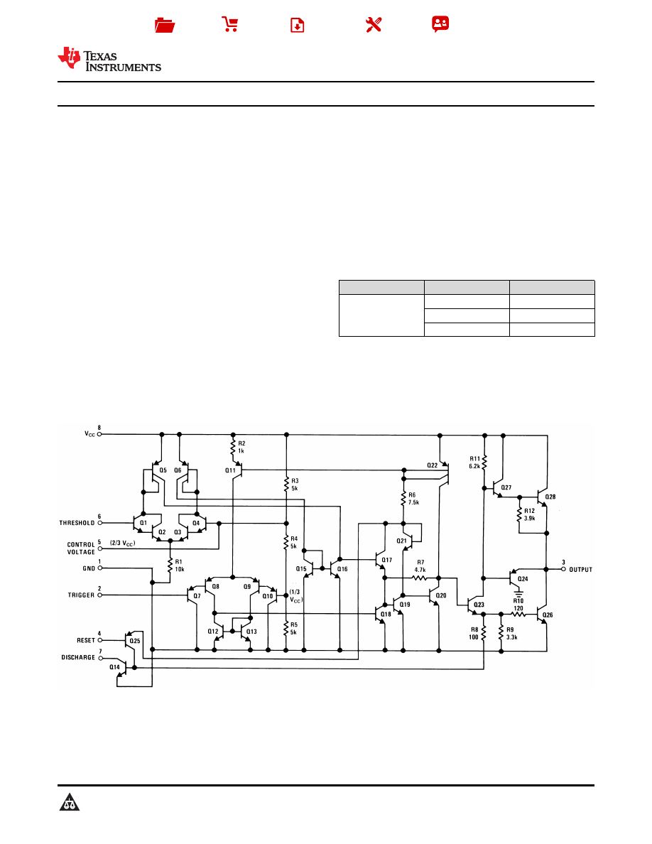
Schematic Diagram
1
An IMPORTANT NOTICE at the end of this data sheet addresses availability, warranty, changes, use in safety-critical applications,
intellectual property matters and other important disclaimers. PRODUCTION DATA.

SNAS548D - FEBRUARY 2000 - REVISED JANUARY 2015
Table of Contents
7.3
Feature Description...................................................
1
Features ..................................................................
7.4
Device Functional Modes..........................................
2
Applications ...........................................................
8
Application and Implementation ........................
3
Description .............................................................
8.1
Application Information............................................
4
Revision History.....................................................
8.2
Typical Application .................................................
5
Pin Configuration and Functions .........................
9
Power Supply Recommendations ......................
6
Specifications.........................................................
10
Layout...................................................................
6.1
Absolute Maximum Ratings ......................................
10.1
Layout Guidelines .................................................
6.2
ESD Ratings..............................................................
10.2
Layout Example ....................................................
6.3
Recommended Operating Conditions .......................
11
Device and Documentation Support .................
6.4
Thermal Information .................................................
11.1
Trademarks ...........................................................
6.5
Electrical Characteristics ..........................................
11.2
Electrostatic Discharge Caution ............................
6.6
Typical Characteristics ..............................................
11.3
Glossary ................................................................
7
Detailed Description ..............................................
12
Mechanical, Packaging, and Orderable
7.1
Overview ...................................................................
Information ...........................................................
7.2
Functional Block Diagram .........................................
4 Revision History
Changes from Revision C (March 2013) to Revision D
Page
Added Pin Configuration and Functions section, ESD Ratings table, Feature Description section, Device Functional
Modes, Application and Implementation section, Power Supply Recommendations section, Layout section, Device
and Documentation Support section, and Mechanical, Packaging, and Orderable Information section ..............................
Changes from Revision B (March 2013) to Revision C
Page
Changed layout of National Data Sheet to TI format ...........................................................................................................
2
Copyright © 2000-2015, Texas Instruments Incorporated
Product Folder Links:
R
R
R
GND
TRIGGER
OUTPUT
RESET
1
2
3
4
+V
CC
DISCHARGE
THRESHOLD
CONTROL
VOLTAGE
8
7
6
5
COMPAR-
ATOR
COMPAR-
ATOR
FLIP FLOP
OUTPUT
STAGE
VREF (INT)
SNAS548D - FEBRUARY 2000 - REVISED JANUARY 2015
5 Pin Configuration and Functions
D, P, and DGK Packages
8-Pin PDIP, SOIC, and VSSOP
Top View
Pin Functions
PIN
I/O
DESCRIPTION
NO.
NAME
Control
Controls the threshold and trigger levels. It determines the pulse width of the output
5
Voltage
I
waveform. An external voltage applied to this pin can also be used to modulate the output
waveform
Discharge
Open collector output which discharges a capacitor between intervals (in phase with output).
7
I
It toggles the output from high to low when voltage reaches 2/3 of the supply voltage
1
GND
O
Ground reference voltage
3
Output
O
Output driven waveform
Reset
Negative pulse applied to this pin to disable or reset the timer. When not used for reset
4
I
purposes, it should be connected to VCC to avoid false triggering
Threshold
Compares the voltage applied to the terminal with a reference voltage of 2/3 Vcc. The
6
I
amplitude of voltage applied to this terminal is responsible for the set state of the flip-flop
Trigger
Responsible for transition of the flip-flop from set to reset. The output of the timer depends
2
I
on the amplitude of the external trigger pulse applied to this pin
8
V
+
I
Supply voltage with respect to GND
Copyright © 2000-2015, Texas Instruments Incorporated
3
Product Folder Links:
SNAS548D - FEBRUARY 2000 - REVISED JANUARY 2015
6 Specifications
6.1 Absolute Maximum Ratings
over operating free-air temperature range (unless otherwise noted)
(1) (2)
MIN
MAX
UNIT
LM555CM, LM555CN
(4)
1180
mW
Power Dissipation
(3)
LM555CMM
613
mW
PDIP Package
Soldering (10 Seconds)
260
°C
Soldering
Vapor Phase (60 Seconds)
215
°C
Small Outline Packages (SOIC and
Information
VSSOP)
Infrared (15 Seconds)
220
°C
Storage temperature, T
stg
-65
150
°C
(1)
Stresses beyond those listed under Absolute Maximum Ratings may cause permanent damage to the device. These are stress ratings
only, which do not imply functional operation of the device at these or any other conditions beyond those indicated under Recommended
Operating Conditions. Exposure to absolute-maximum-rated conditions for extended periods may affect device reliability.
(2)
If Military/Aerospace specified devices are required, please contact the TI Sales Office/Distributors for availability and specifications.
(3)
For operating at elevated temperatures the device must be derated above 25 °C based on a 150 °C maximum junction temperature and a
thermal resistance of 106 °C/W (PDIP), 170 °C/W (S0IC-8), and 204 °C/W (VSSOP) junction to ambient.
(4)
Refer to RETS555X drawing of military LM555H and LM555J versions for specifications.
6.2 ESD Ratings
VALUE
UNIT
V
(ESD)
Electrostatic discharge
Human-body model (HBM), per ANSI/ESDA/JEDEC JS-001
(1)
±500
(2)
V
(1)
JEDEC document JEP155 states that 500-V HBM allows safe manufacturing with a standard ESD control process.
(2)
The ESD information listed is for the SOIC package.
6.3 Recommended Operating Conditions
over operating free-air temperature range (unless otherwise noted)
MIN
MAX
UNIT
Supply Voltage
18
V
Temperature, T
A
0
70
°C
Operating junction temperature, T
J
70
°C
6.4 Thermal Information
LM555
THERMAL METRIC
(1)
PDIP
SOIC
VSSOP
UNIT
8 PINS
R
ΘJA
Junction-to-ambient thermal resistance
106
170
204
°C/W
(1)
For more information about traditional and new thermal metrics, see the IC Package Thermal Metrics application report,
4
Copyright © 2000-2015, Texas Instruments Incorporated
Product Folder Links:
SNAS548D - FEBRUARY 2000 - REVISED JANUARY 2015
6.5 Electrical Characteristics
(T
A
= 25 °C, V
CC
= 5 V to 15 V, unless otherwise specified)
(1) (2)
PARAMETER
TEST CONDITIONS
MIN
TYP
MAX
UNIT
Supply Voltage
4.5
16
V
Supply Current
V
CC
= 5 V, R
L
=
3
6
mA
V
CC
= 15 V, R
L
=
10
15
(Low State)
(3)
Timing Error, Monostable
Initial Accuracy
1 %
Drift with Temperature
R
A
= 1 k to 100 k
Ω,
50
ppm/ °C
C = 0.1
μF,
(4)
Accuracy over Temperature
1.5 %
Drift with Supply
0.1 %
V
Timing Error, Astable
Initial Accuracy
2.25
Drift with Temperature
R
A
, R
B
=1 k to 100 k
Ω,
150
ppm/ °C
C = 0.1
μF,
(4)
Accuracy over Temperature
3.0%
Drift with Supply
0.30 %
/V
Threshold Voltage
0.667
x V
CC
Trigger Voltage
V
CC
= 15 V
5
V
V
CC
= 5 V
1.67
V
Trigger Current
0.5
0.9
μA
Reset Voltage
0.4
0.5
1
V
Reset Current
0.1
0.4
mA
Threshold Current
(5)
0.1
0.25
μA
Control Voltage Level
V
CC
= 15 V
9
10
11
V
V
CC
= 5 V
2.6
3.33
4
Pin 7 Leakage Output High
1
100
nA
Pin 7 Sat
(6)
Output Low
V
CC
= 15 V, I
7
= 15 mA
180
mV
Output Low
V
CC
= 4.5 V, I
7
= 4.5 mA
80
200
mV
Output Voltage Drop (Low)
V
CC
= 15 V
I
SINK
= 10 mA
0.1
0.25
V
I
SINK
= 50 mA
0.4
0.75
V
I
SINK
= 100 mA
2
2.5
V
I
SINK
= 200 mA
2.5
V
V
CC
= 5 V
I
SINK
= 8 mA
V
I
SINK
= 5 mA
0.25
0.35
V
(1)
All voltages are measured with respect to the ground pin, unless otherwise specified.
(2)
indicate limits beyond which damage to the device may occur.
indicate
conditions for which the device is functional, but do not ensure specific performance limits.
state DC and AC
electrical specifications under particular test conditions which ensures specific performance limits. This assumes that the device is within
the
. Specifications are not ensured for parameters where no limit is given, however, the typical
value is a good indication of device performance.
(3)
Supply current when output high typically 1 mA less at V
CC
= 5 V.
(4)
Tested at V
CC
= 5 V and V
CC
= 15 V.
(5)
This will determine the maximum value of R
A
+ R
B
for 15 V operation. The maximum total (R
A
+ R
B
) is 20 M
Ω.
(6)
No protection against excessive pin 7 current is necessary providing the package dissipation rating will not be exceeded.
Copyright © 2000-2015, Texas Instruments Incorporated
5
Product Folder Links:
SNAS548D - FEBRUARY 2000 - REVISED JANUARY 2015
Electrical Characteristics (continued)
(T
A
= 25 °C, V
CC
= 5 V to 15 V, unless otherwise specified)
PARAMETER
TEST CONDITIONS
MIN
TYP
MAX
UNIT
Output Voltage Drop (High)
I
SOURCE
= 200 mA, V
CC
= 15 V
12.5
V
I
SOURCE
= 100 mA, V
CC
= 15 V
12.75
13.3
V
V
CC
= 5 V
2.75
3.3
V
Rise Time of Output
100
ns
Fall Time of Output
100
ns
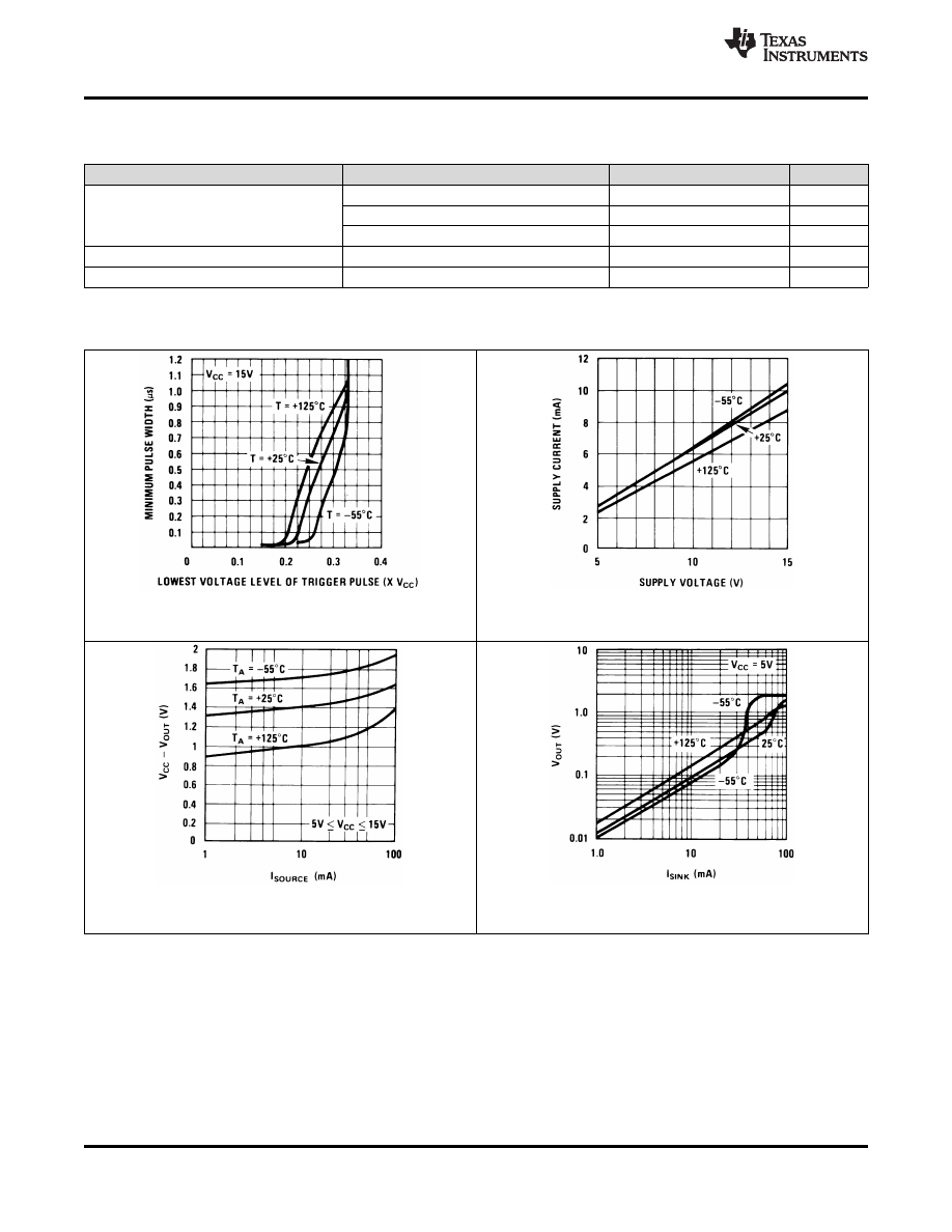
6.6 Typical Characteristics
Figure 2. Supply Current vs. Supply Voltage
Figure 1. Minimum Pulse Width Required For Triggering
Figure 4. Low Output Voltage vs. Output Sink Current
Figure 3. High Output Voltage vs. Output Source Current
6
Copyright © 2000-2015, Texas Instruments Incorporated
Product Folder Links:
SNAS548D - FEBRUARY 2000 - REVISED JANUARY 2015
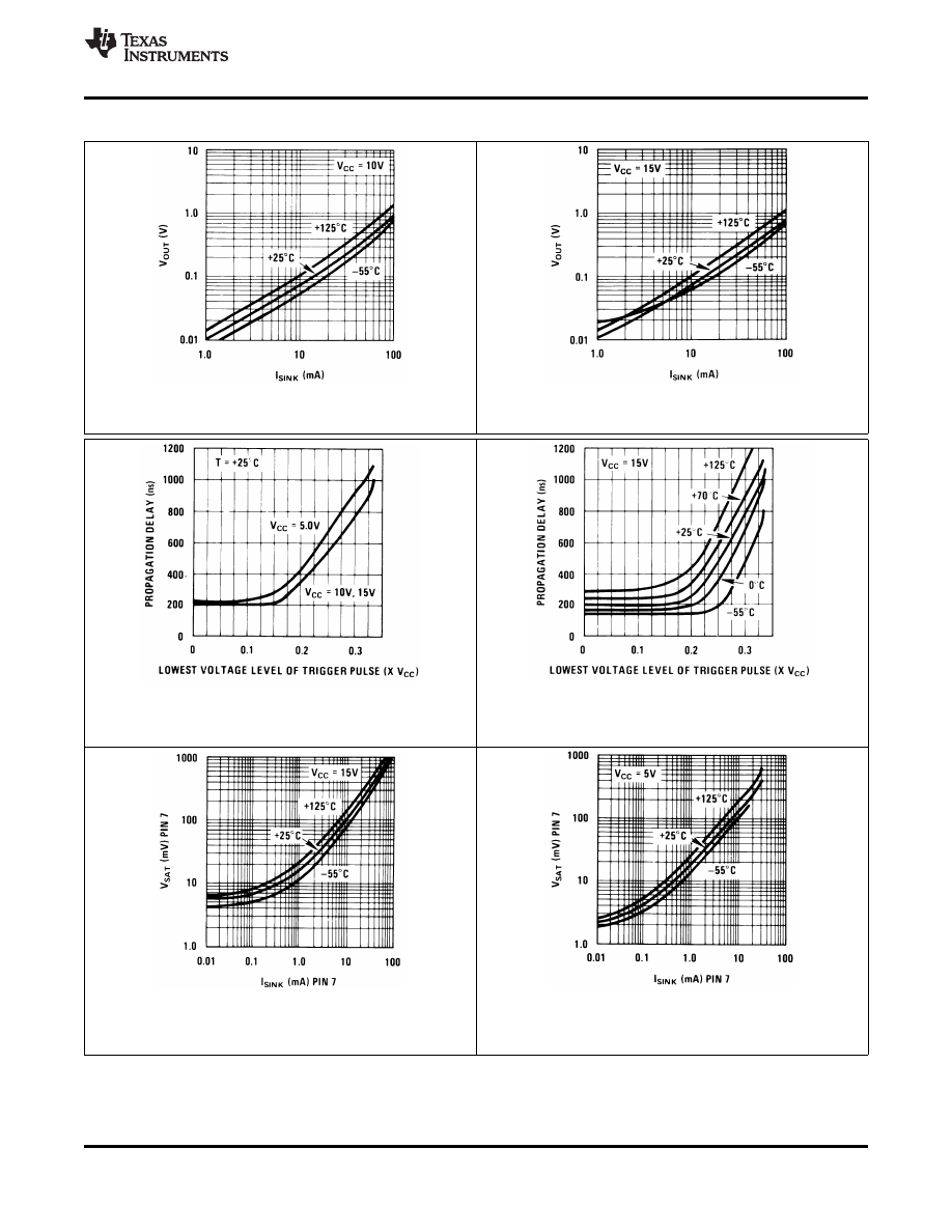
Typical Characteristics (continued)
Figure 6. Low Output Voltage vs. Output Sink Current
Figure 5. Low Output Voltage vs. Output Sink Current
Figure 8. Output Propagation Delay vs. Voltage Level of
Figure 7. Output Propagation Delay vs. Voltage Level of
Trigger Pulse
Trigger Pulse
Figure 10. Discharge Transistor (Pin 7) Voltage vs. Sink
Figure 9. Discharge Transistor (Pin 7) Voltage vs. Sink
Current
Current
Copyright © 2000-2015, Texas Instruments Incorporated
7
Product Folder Links:
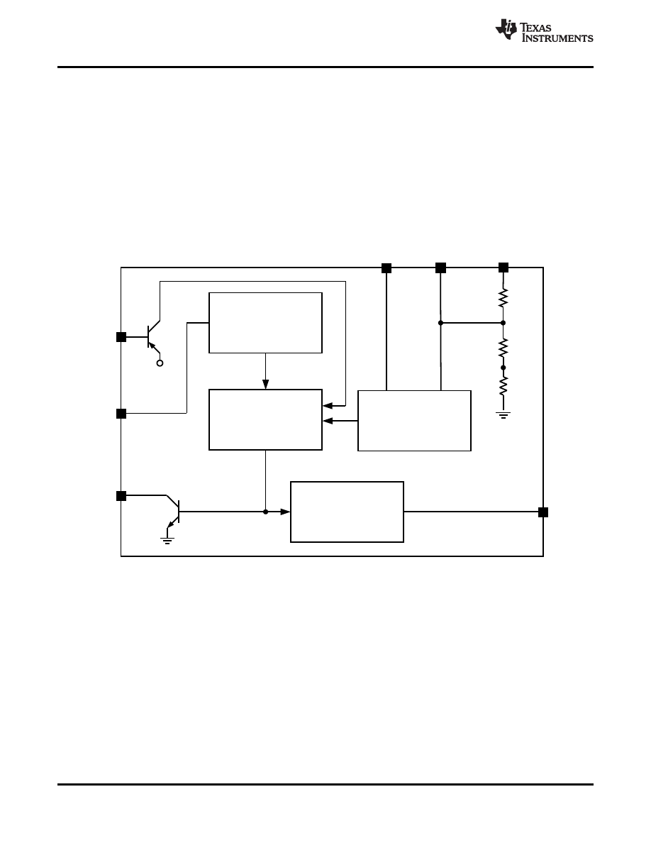
COMPARATOR
TRIGGER
FLIP FLOP
COMPARATOR
RESET
+Vcc
DISCHARGE
THRESHOLD
V
ref
(int)
OUTPUT
STAGE
CONTROL
VOLTAGE
OUTPUT
SNAS548D - FEBRUARY 2000 - REVISED JANUARY 2015
7 Detailed Description
7.1 Overview
The LM555 is a highly stable device for generating accurate time delays or oscillation. Additional terminals are
provided for triggering or resetting if desired. In the time delay mode of operation, the time is precisely controlled
by one external resistor and capacitor. For astable operation as an oscillator, the free running frequency and duty
cycle are accurately controlled with two external resistors and one capacitor. The circuit may be triggered and
reset on falling waveforms, and the output circuit can source or sink up to 200mA or driver TTL circuits. The
LM555 are available in 8-pin PDIP, SOIC, and VSSOP packages and is a direct replacement for SE555/NE555.
7.2 Functional Block Diagram
7.3 Feature Description
7.3.1 Direct Replacement for SE555/NE555
The LM555 timer is a direct replacement for SE555 and NE555. It is pin-to-pin compatible so that no schematic
or layout changes are necessary. The LM555 come in an 8-pin PDIP, SOIC, and VSSOP package.
7.3.2 Timing From Microseconds Through Hours
The LM555 has the ability to have timing parameters from the microseconds range to hours. The time delay of
the system can be determined by the time constant of the R and C value used for either the monostable or
astable configuration. A nomograph is available for easy determination of R and C values for various time delays.
7.3.3 Operates in Both Astable and Monostable Mode
The LM555 can operate in both astable and monostable mode depending on the application requirements.
Monostable mode: The LM555 timer acts as a one-shot pulse generator. The pulse beings when the LM555
timer receives a signal at the trigger input that falls below a 1/3 of the voltage supply. The width of the output
pulse is determined by the time constant of an RC network. The output pulse ends when the voltage on the
8
Copyright © 2000-2015, Texas Instruments Incorporated
Product Folder Links:
SNAS548D - FEBRUARY 2000 - REVISED JANUARY 2015
Feature Description (continued)
capacitor equals 2/3 of the supply voltage. The output pulse width can be extended or shortened depending
on the application by adjusting the R and C values.
Astable (free-running) mode: The LM555 timer can operate as an oscillator and puts out a continuous stream
of rectangular pulses having a specified frequency. The frequency of the pulse stream depends on the values
of R
A
, R
B
, and C.
7.4 Device Functional Modes
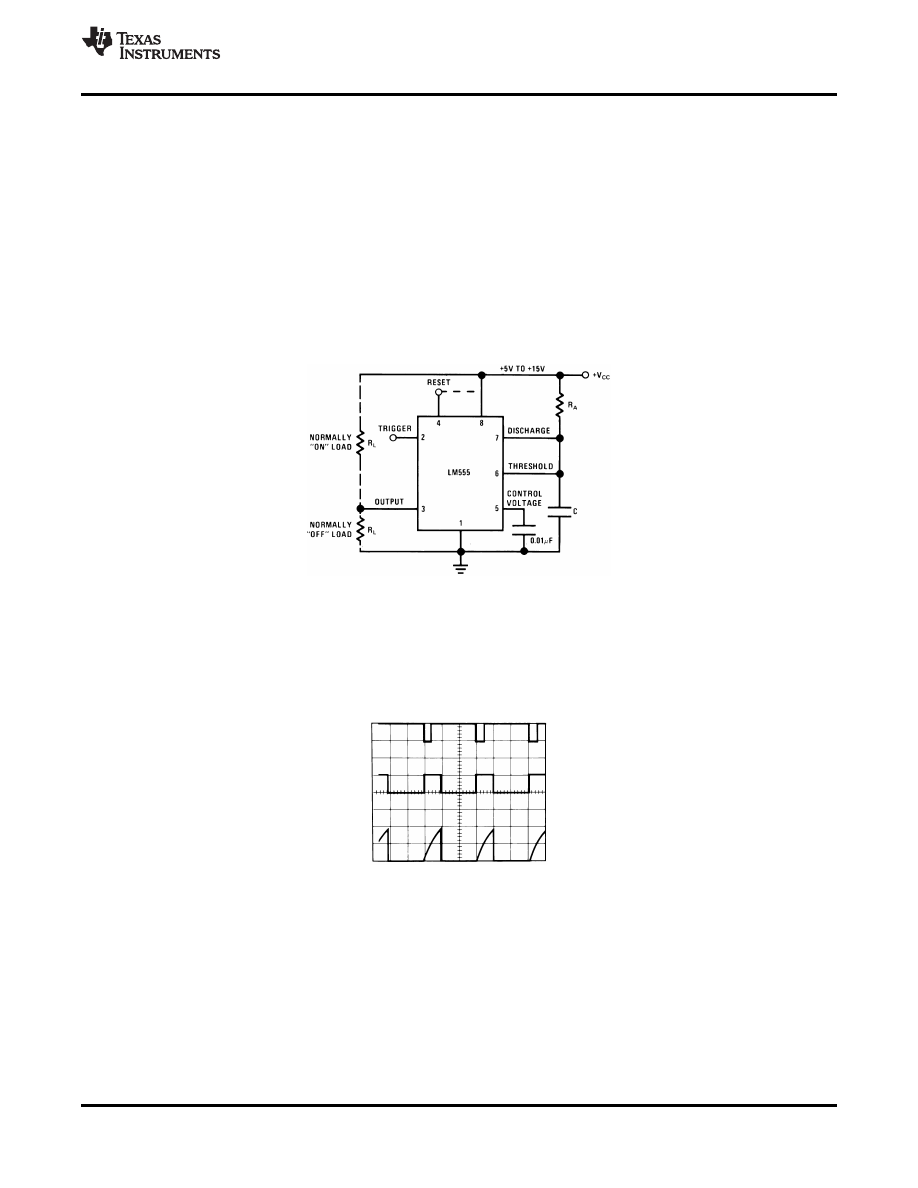
7.4.1 Monostable Operation
In this mode of operation, the timer functions as a one-shot
). The external capacitor is initially held
discharged by a transistor inside the timer. Upon application of a negative trigger pulse of less than 1/3 V
CC
to
pin 2, the flip-flop is set which both releases the short circuit across the capacitor and drives the output high.
Figure 11. Monostable
The voltage across the capacitor then increases exponentially for a period of t = 1.1 R
A
C, at the end of which
time the voltage equals 2/3 V
CC
. The comparator then resets the flip-flop which in turn discharges the capacitor
and drives the output to its low state.
shows the waveforms generated in this mode of operation. Since
the charge and the threshold level of the comparator are both directly proportional to supply voltage, the timing
interval is independent of supply.
V
CC
= 5 V
Top Trace: Input 5V/Div.
TIME = 0.1 ms/DIV.
Middle Trace: Output 5V/Div.
R
A
= 9.1 k
Ω
Bottom Trace: Capacitor Voltage 2V/Div.
C = 0.01
μF
Figure 12. Monostable Waveforms
During the timing cycle when the output is high, the further application of a trigger pulse will not effect the circuit
so long as the trigger input is returned high at least 10
μs before the end of the timing interval. However the
circuit can be reset during this time by the application of a negative pulse to the reset terminal (pin 4). The output
will then remain in the low state until a trigger pulse is again applied.
When the reset function is not in use, TI recommends connecting the Reset pin to V
CC
to avoid any possibility of
false triggering.
Copyright © 2000-2015, Texas Instruments Incorporated
9
Product Folder Links:
SNAS548D - FEBRUARY 2000 - REVISED JANUARY 2015
Device Functional Modes (continued)
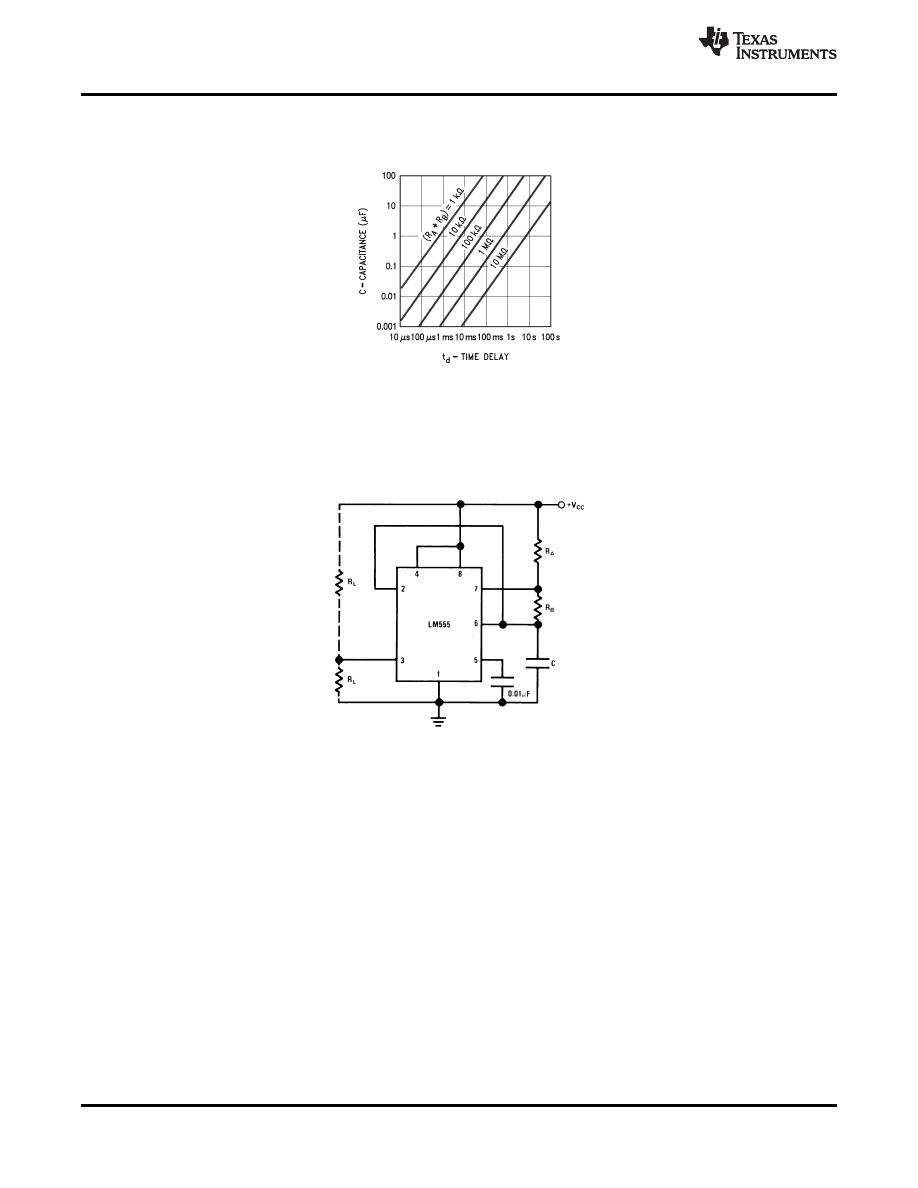
is a nomograph for easy determination of R, C values for various time delays.
Figure 13. Time Delay
7.4.2 Astable Operation
If the circuit is connected as shown in
(pins 2 and 6 connected) it will trigger itself and free run as a
multivibrator. The external capacitor charges through R
A
+ R
B
and discharges through R
B
. Thus the duty cycle
may be precisely set by the ratio of these two resistors.
Figure 14. Astable
In this mode of operation, the capacitor charges and discharges between 1/3 V
CC
and 2/3 V
CC
. As in the
triggered mode, the charge and discharge times, and therefore the frequency are independent of the supply
voltage.
shows the waveforms generated in this mode of operation.
10
Copyright © 2000-2015, Texas Instruments Incorporated
Product Folder Links:

SNAS548D - FEBRUARY 2000 - REVISED JANUARY 2015
Device Functional Modes (continued)
V
CC
= 5 V
Top Trace: Output 5V/Div.
TIME = 20
μs/DIV.
Bottom Trace: Capacitor Voltage 1V/Div.
R
A
= 3.9 k
Ω
R
B
= 3 k
Ω
C = 0.01
μF
Figure 15. Astable Waveforms
The charge time (output high) is given by:
t
1
= 0.693 (R
A
+ R
B
) C
(1)
And the discharge time (output low) by:
t
2
= 0.693 (R
B
) C
(2)
Thus the total period is:
T = t
1
+ t
2
= 0.693 (R
A
+2R
B
) C
(3)
The frequency of oscillation is:
(4)
may be used for quick determination of these RC values.
The duty cycle is:
(5)
Figure 16. Free Running Frequency
Copyright © 2000-2015, Texas Instruments Incorporated
11
Product Folder Links:
SNAS548D - FEBRUARY 2000 - REVISED JANUARY 2015
8 Application and Implementation
NOTE
Information in the following applications sections is not part of the TI component
specification, and TI does not warrant its accuracy or completeness. TIs customers are
responsible for determining suitability of components for their purposes. Customers should
validate and test their design implementation to confirm system functionality.
8.1 Application Information
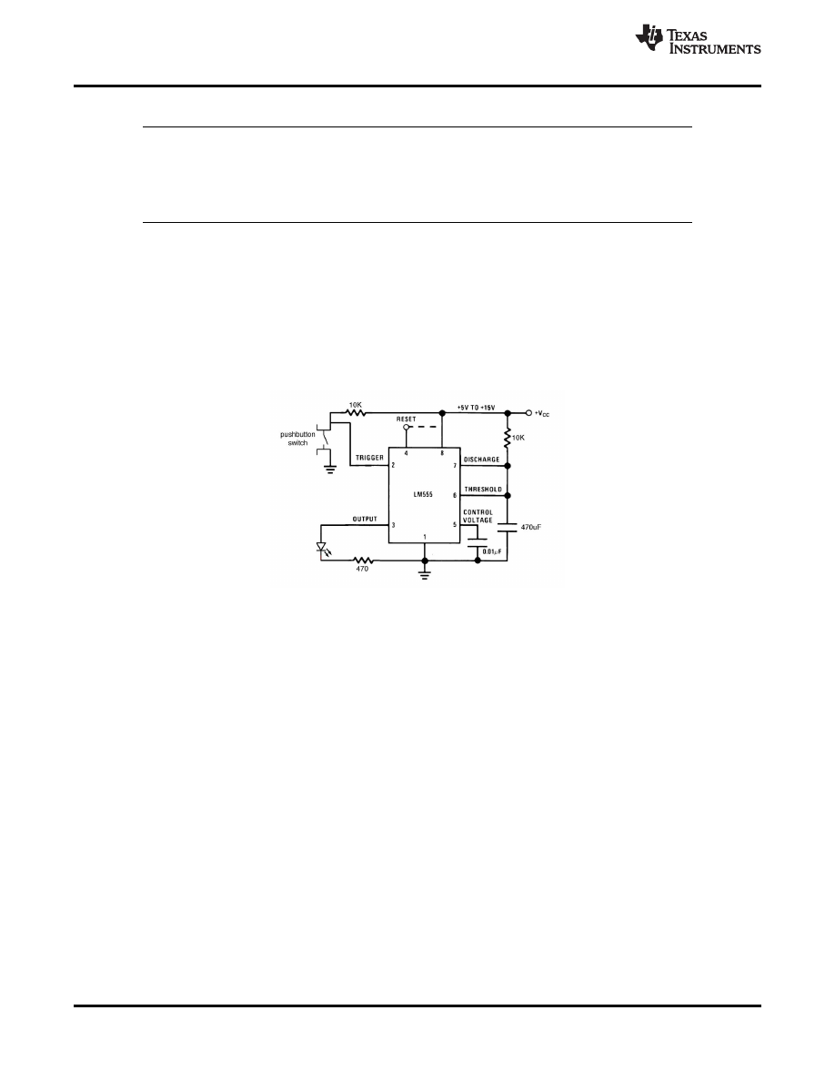
The LM555 timer can be used a various configurations, but the most commonly used configuration is in
monostable mode. A typical application for the LM555 timer in monostable mode is to turn on an LED for a
specific time duration. A pushbutton is used as the trigger to output a high pulse when trigger pin is pulsed low.
This simple application can be modified to fit any application requirement.
8.2 Typical Application
shows the schematic of the LM555 that flashes an LED in monostable mode.
Figure 17. Schematic of Monostable Mode to Flash an LED
8.2.1 Design Requirements
The main design requirement for this application requires calculating the duration of time for which the output
stays high. The duration of time is dependent on the R and C values (as shown in
) and can be
calculated by:
t = 1.1 × R × C seconds
(6)
8.2.2 Detailed Design Procedure
To allow the LED to flash on for a noticeable amount of time, a 5 second time delay was chosen for this
application. By using
, RC equals 4.545. If R is selected as 100 k
Ω, C = 45.4 µF. The values of R =
100 k
Ω and C = 47 µF was selected based on standard values of resistors and capacitors. A momentary push
button switch connected to ground is connected to the trigger input with a 10-K current limiting resistor pullup to
the supply voltage. When the push button is pressed, the trigger pin goes to GND. An LED is connected to the
output pin with a current limiting resistor in series from the output of the LM555 to GND. The reset pin is not used
and was connected to the supply voltage.
8.2.2.1 Frequency Divider
The monostable circuit of
can be used as a frequency divider by adjusting the length of the timing
cycle.
shows the waveforms generated in a divide by three circuit.
12
Copyright © 2000-2015, Texas Instruments Incorporated
Product Folder Links:

SNAS548D - FEBRUARY 2000 - REVISED JANUARY 2015
Typical Application (continued)
V
CC
= 5 V
Top Trace: Input 4 V/Div.
TIME = 20
μs/DIV.
Middle Trace: Output 2V/Div.
R
A
= 9.1 k
Ω
Bottom Trace: Capa citor 2V/Div.
C = 0.01
μF
Figure 18. Frequency Divider
8.2.2.2 Additional Information
Lower comparator storage time can be as long as 10
μs when pin 2 is driven fully to ground for triggering. This
limits the monostable pulse width to 10
μs minimum.
Delay time reset to output is 0.47
μs typical. Minimum reset pulse width must be 0.3 μs, typical.
Pin 7 current switches within 30 ns of the output (pin 3) voltage.
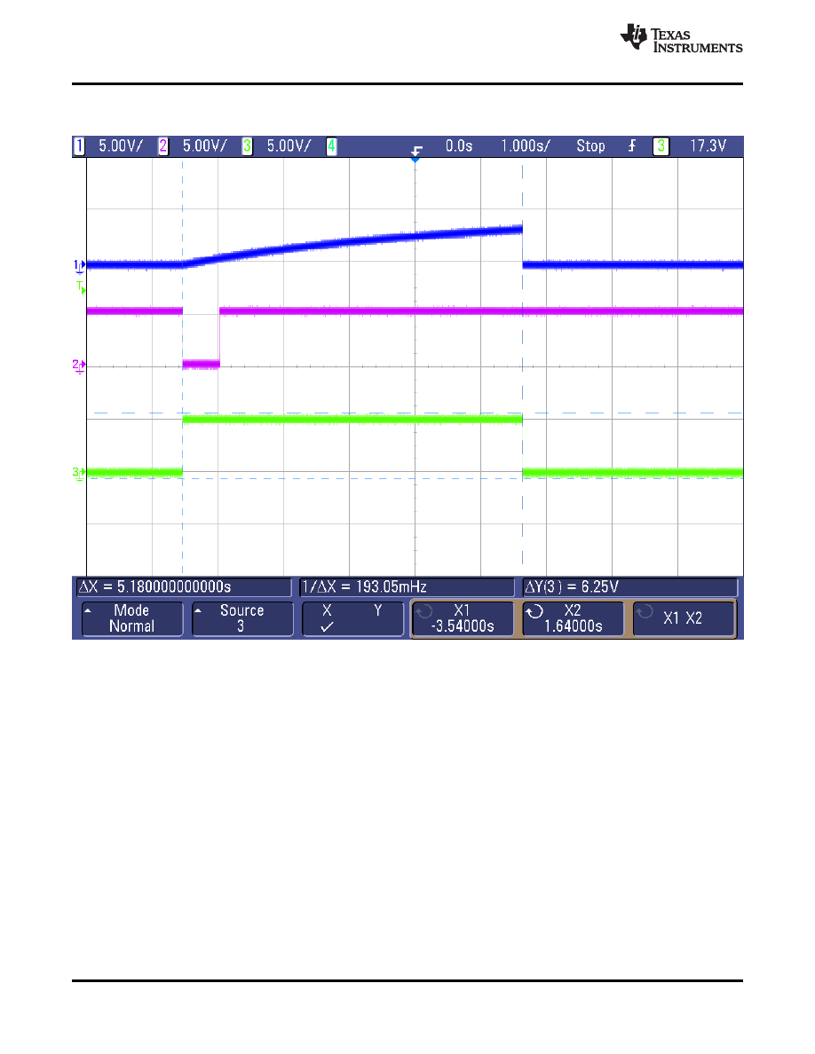
8.2.3 Application Curves
The data shown below was collected with the circuit used in the typical applications section. The LM555 was
configured in the monostable mode with a time delay of 5.17 s. The waveforms correspond to:
Top Waveform (Yellow) - Capacitor voltage
Middle Waveform (Green) - Trigger
Bottom Waveform (Purple) - Output
As the trigger pin pulses low, the capacitor voltage starts charging and the output goes high. The output goes low
as soon as the capacitor voltage reaches 2/3 of the supply voltage, which is the time delay set by the R and C
value. For this example, the time delay is 5.17 s.
Copyright © 2000-2015, Texas Instruments Incorporated
13
Product Folder Links:
SNAS548D - FEBRUARY 2000 - REVISED JANUARY 2015
Typical Application (continued)
Figure 19. Trigger, Capacitor Voltage, and Output Waveforms in Monostable Mode
14
Copyright © 2000-2015, Texas Instruments Incorporated
Product Folder Links:
SNAS548D - FEBRUARY 2000 - REVISED JANUARY 2015
9 Power Supply Recommendations
The LM555 requires a voltage supply within 4.5 V to 16 V. Adequate power supply bypassing is necessary to
protect associated circuitry. The minimum recommended capacitor value is 0.1
μF in parallel with a 1-μF
electrolytic capacitor. Place the bypass capacitors as close as possible to the LM555 and minimize the trace
length.
10 Layout
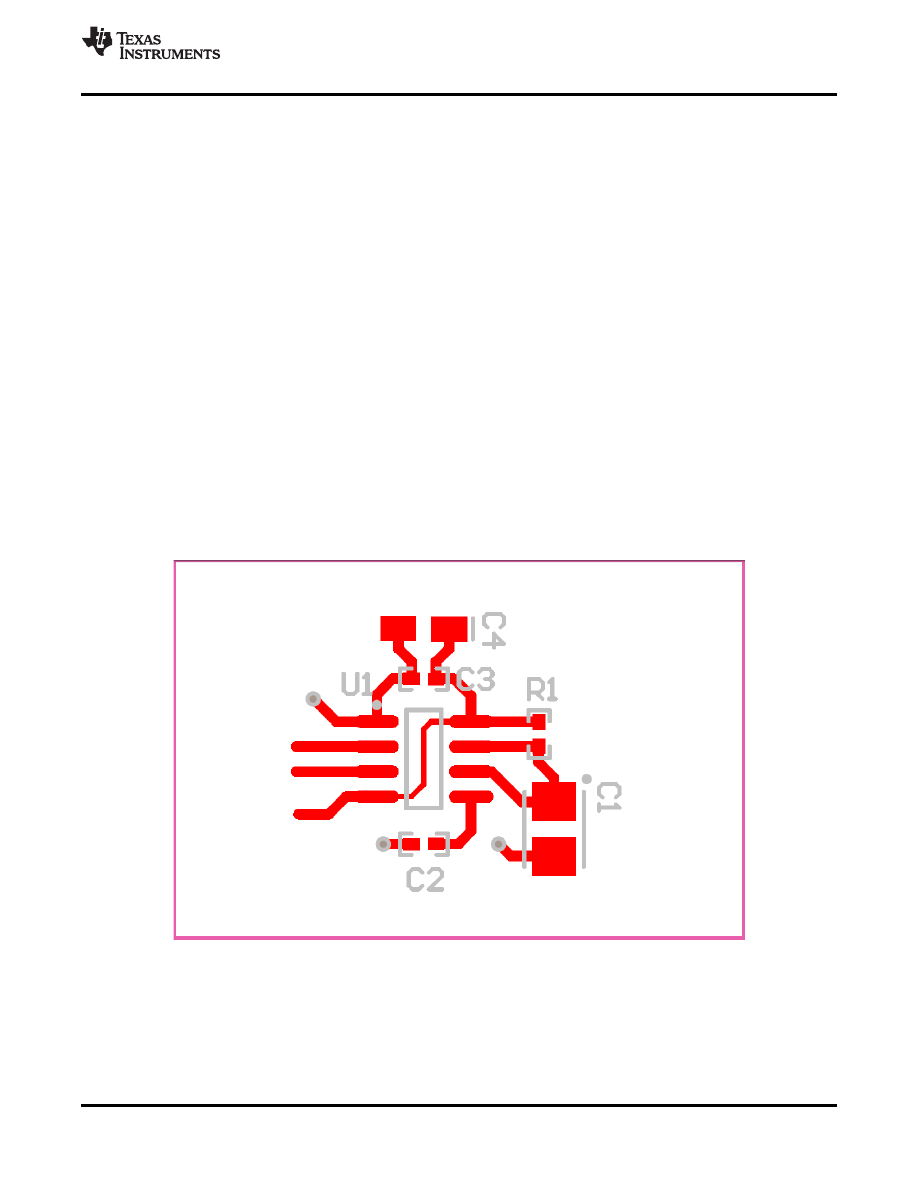
10.1 Layout Guidelines
Standard PCB rules apply to routing the LM555. The 0.1- µF capacitor in parallel with a 1- µF electrolytic capacitor
should be as close as possible to the LM555. The capacitor used for the time delay should also be placed as
close to the discharge pin. A ground plane on the bottom layer can be used to provide better noise immunity and
signal integrity.
is the basic layout for various applications.
C1 - based on time delay calculations
C2 - 0.01- µF bypass capacitor for control voltage pin
C3 - 0.1- µF bypass ceramic capacitor
C4 - 1- µF electrolytic bypass capacitor
R1 - based on time delay calculations
U1 - LMC555
10.2 Layout Example
Figure 20. Layout Example
Copyright © 2000-2015, Texas Instruments Incorporated
15
Product Folder Links:

SNAS548D - FEBRUARY 2000 - REVISED JANUARY 2015
11 Device and Documentation Support
11.1 Trademarks
All trademarks are the property of their respective owners.
11.2 Electrostatic Discharge Caution
These devices have limited built-in ESD protection. The leads should be shorted together or the device placed in conductive foam
during storage or handling to prevent electrostatic damage to the MOS gates.
11.3 Glossary
TI Glossary.
This glossary lists and explains terms, acronyms, and definitions.
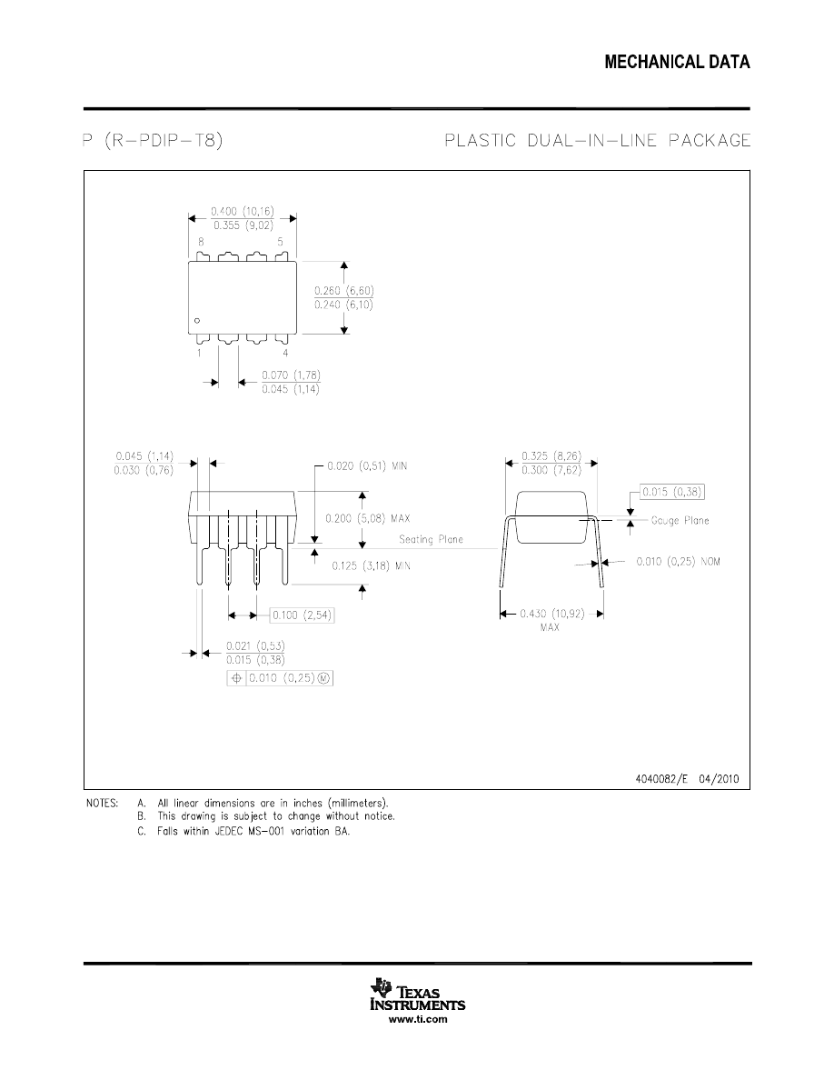
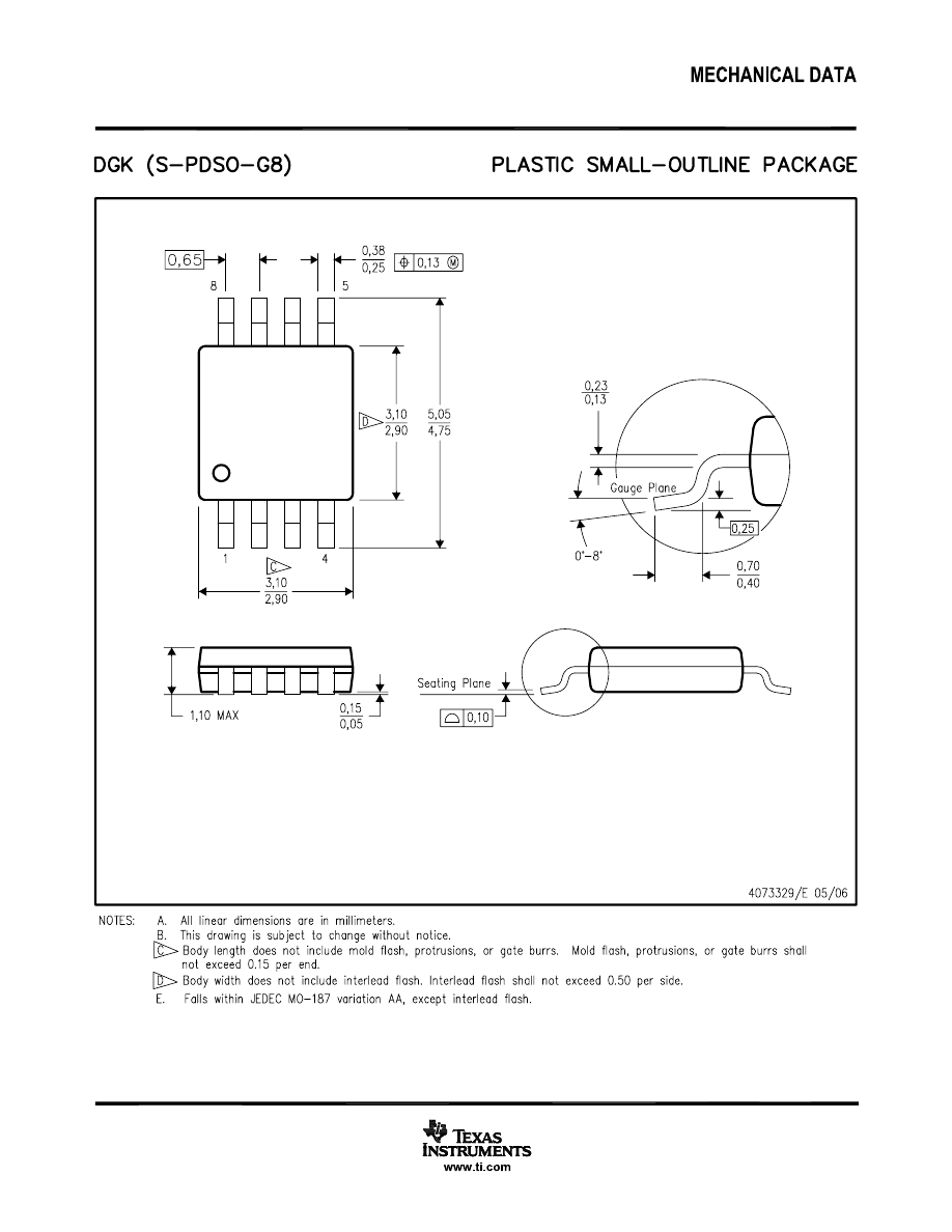
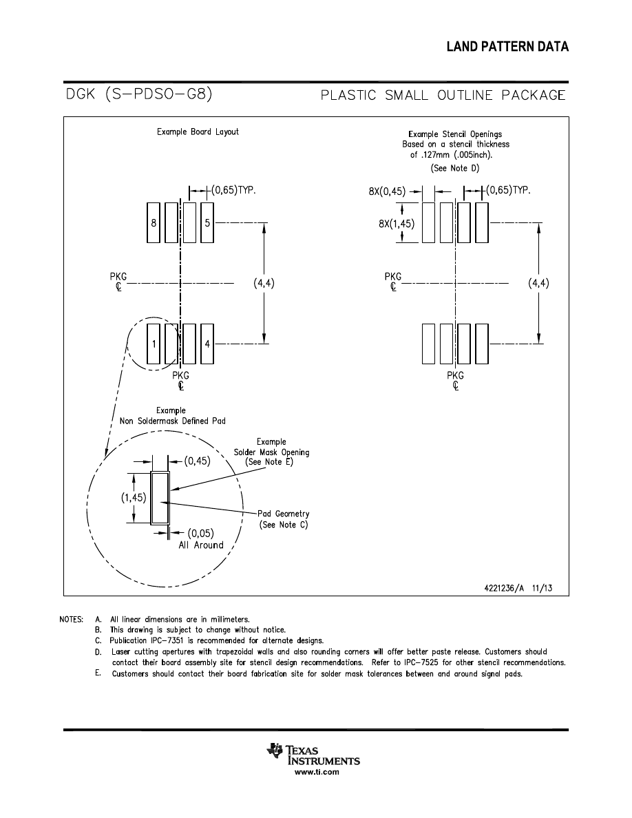
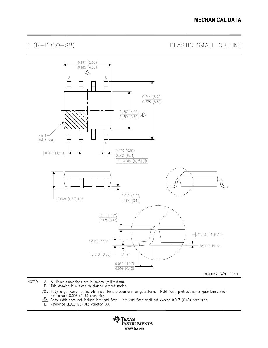
12 Mechanical, Packaging, and Orderable Information
The following pages include mechanical, packaging, and orderable information. This information is the most
current data available for the designated devices. This data is subject to change without notice and revision of
this document. For browser-based versions of this data sheet, refer to the left-hand navigation.
16
Copyright © 2000-2015, Texas Instruments Incorporated
Product Folder Links:
PACKAGE OPTION ADDENDUM
www.ti.com
27-Jul-2016
Addendum-Page 1
PACKAGING INFORMATION
Orderable Device
Status
(1)
Package Type Package
Drawing
Pins Package
Qty
Eco Plan
(2)
Lead/Ball Finish
(6)
MSL Peak Temp
(3)
Op Temp ( °C)
Device Marking
(4/5)
Samples
LM555-MWC
ACTIVE
WAFERSALE
YS
0
1
Green (RoHS
& no Sb/Br)
Call TI
Level-1-NA-UNLIM
-40 to 85
LM555CM
NRND
SOIC
D
8
95
TBD
Call TI
Call TI
0 to 70
LM
555CM
LM555CM/NOPB
ACTIVE
SOIC
D
8
95
Green (RoHS
& no Sb/Br)
CU SN
Level-1-260C-UNLIM
0 to 70
LM
555CM
LM555CMM
NRND
VSSOP
DGK
8
1000
TBD
Call TI
Call TI
0 to 70
Z55
LM555CMM/NOPB
ACTIVE
VSSOP
DGK
8
1000
Green (RoHS
& no Sb/Br)
CU SN
Level-1-260C-UNLIM
0 to 70
Z55
LM555CMMX/NOPB
ACTIVE
VSSOP
DGK
8
3500
Green (RoHS
& no Sb/Br)
CU SN
Level-1-260C-UNLIM
0 to 70
Z55
LM555CMX
NRND
SOIC
D
8
2500
TBD
Call TI
Call TI
0 to 70
LM
555CM
LM555CMX/NOPB
ACTIVE
SOIC
D
8
2500
Green (RoHS
& no Sb/Br)
CU SN
Level-1-260C-UNLIM
0 to 70
LM
555CM
LM555CN/NOPB
ACTIVE
PDIP
P
8
40
Green (RoHS
& no Sb/Br)
CU SN
Level-1-NA-UNLIM
0 to 70
LM
555CN
MC1455P1
OBSOLETE
PDIP
P
8
TBD
Call TI
Call TI
0 to 70
LM
555CN
NE555V
OBSOLETE
PDIP
P
8
TBD
Call TI
Call TI
0 to 70
LM
555CN
(1)
The marketing status values are defined as follows:
ACTIVE: Product device recommended for new designs.
LIFEBUY: TI has announced that the device will be discontinued, and a lifetime-buy period is in effect.
NRND: Not recommended for new designs. Device is in production to support existing customers, but TI does not recommend using this part in a new design.
PREVIEW: Device has been announced but is not in production. Samples may or may not be available.
OBSOLETE: TI has discontinued the production of the device.
(2)
Eco Plan - The planned eco-friendly classification: Pb-Free (RoHS), Pb-Free (RoHS Exempt), or Green (RoHS & no Sb/Br) - please check
for the latest availability
information and additional product content details.
TBD: The Pb-Free/Green conversion plan has not been defined.
Pb-Free (RoHS): TI's terms "Lead-Free" or "Pb-Free" mean semiconductor products that are compatible with the current RoHS requirements for all 6 substances, including the requirement that
lead not exceed 0.1% by weight in homogeneous materials. Where designed to be soldered at high temperatures, TI Pb-Free products are suitable for use in specified lead-free processes.
Pb-Free (RoHS Exempt): This component has a RoHS exemption for either 1) lead-based flip-chip solder bumps used between the die and package, or 2) lead-based die adhesive used between
the die and leadframe. The component is otherwise considered Pb-Free (RoHS compatible) as defined above.
PACKAGE OPTION ADDENDUM
www.ti.com
27-Jul-2016
Addendum-Page 2
Green (RoHS & no Sb/Br): TI defines "Green" to mean Pb-Free (RoHS compatible), and free of Bromine (Br) and Antimony (Sb) based flame retardants (Br or Sb do not exceed 0.1% by weight
in homogeneous material)
(3)
MSL, Peak Temp. - The Moisture Sensitivity Level rating according to the JEDEC industry standard classifications, and peak solder temperature.
(4)
There may be additional marking, which relates to the logo, the lot trace code information, or the environmental category on the device.
(5)
Multiple Device Markings will be inside parentheses. Only one Device Marking contained in parentheses and separated by a "~" will appear on a device. If a line is indented then it is a continuation
of the previous line and the two combined represent the entire Device Marking for that device.
(6)
Lead/Ball Finish - Orderable Devices may have multiple material finish options. Finish options are separated by a vertical ruled line. Lead/Ball Finish values may wrap to two lines if the finish
value exceeds the maximum column width.
Important Information and Disclaimer:The information provided on this page represents TI's knowledge and belief as of the date that it is provided. TI bases its knowledge and belief on information
provided by third parties, and makes no representation or warranty as to the accuracy of such information. Efforts are underway to better integrate information from third parties. TI has taken and
continues to take reasonable steps to provide representative and accurate information but may not have conducted destructive testing or chemical analysis on incoming materials and chemicals.
TI and TI suppliers consider certain information to be proprietary, and thus CAS numbers and other limited information may not be available for release.
In no event shall TI's liability arising out of such information exceed the total purchase price of the TI part(s) at issue in this document sold by TI to Customer on an annual basis.
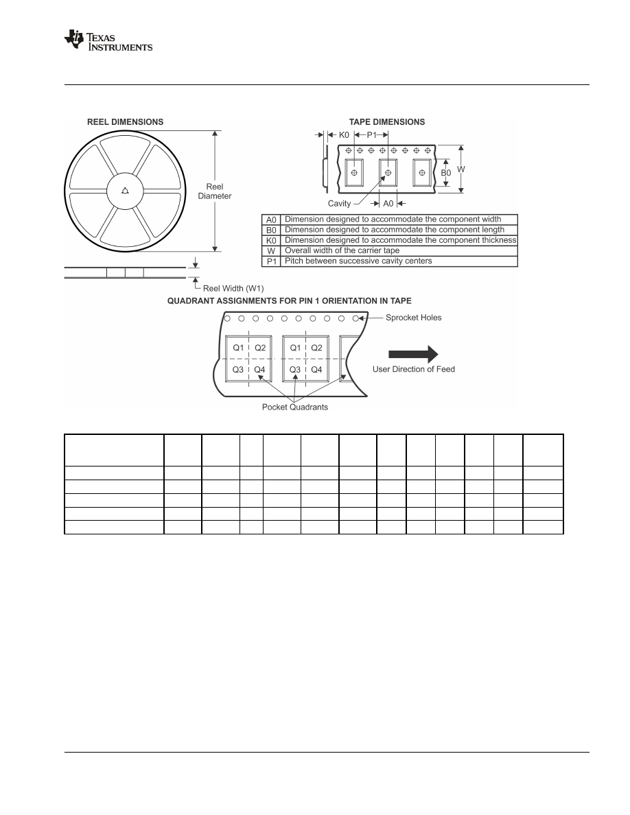
TAPE AND REEL INFORMATION
*All dimensions are nominal
Device
Package
Type
Package
Drawing
Pins
SPQ
Reel
Diameter
(mm)
Reel
Width
W1 (mm)
A0
(mm)
B0
(mm)
K0
(mm)
P1
(mm)
W
(mm)
Pin1
Quadrant
LM555CMM
VSSOP
DGK
8
1000
178.0
12.4
5.3
3.4
1.4
8.0
12.0
Q1
LM555CMM/NOPB
VSSOP
DGK
8
1000
178.0
12.4
5.3
3.4
1.4
8.0
12.0
Q1
LM555CMMX/NOPB
VSSOP
DGK
8
3500
330.0
12.4
5.3
3.4
1.4
8.0
12.0
Q1
LM555CMX
SOIC
D
8
2500
330.0
12.4
6.5
5.4
2.0
8.0
12.0
Q1
LM555CMX/NOPB
SOIC
D
8
2500
330.0
12.4
6.5
5.4
2.0
8.0
12.0
Q1
PACKAGE MATERIALS INFORMATION
www.ti.com
21-Oct-2014
Pack Materials-Page 1
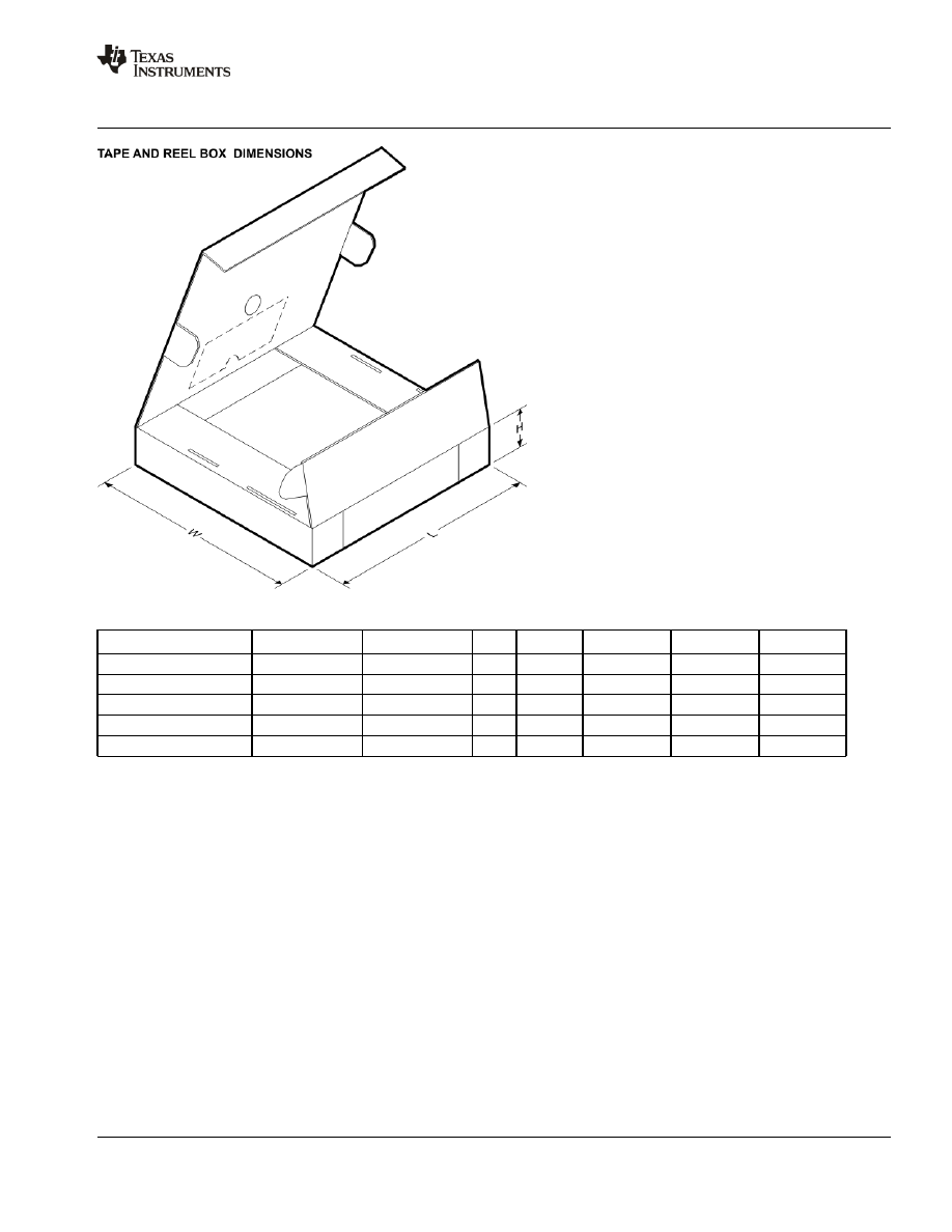
*All dimensions are nominal
Device
Package Type
Package Drawing
Pins
SPQ
Length (mm)
Width (mm)
Height (mm)
LM555CMM
VSSOP
DGK
8
1000
210.0
185.0
35.0
LM555CMM/NOPB
VSSOP
DGK
8
1000
210.0
185.0
35.0
LM555CMMX/NOPB
VSSOP
DGK
8
3500
367.0
367.0
35.0
LM555CMX
SOIC
D
8
2500
367.0
367.0
35.0
LM555CMX/NOPB
SOIC
D
8
2500
367.0
367.0
35.0
PACKAGE MATERIALS INFORMATION
www.ti.com
21-Oct-2014
Pack Materials-Page 2

IMPORTANT NOTICE
Texas Instruments Incorporated and its subsidiaries (TI) reserve the right to make corrections, enhancements, improvements and other
changes to its semiconductor products and services per JESD46, latest issue, and to discontinue any product or service per JESD48, latest
issue. Buyers should obtain the latest relevant information before placing orders and should verify that such information is current and
complete. All semiconductor products (also referred to herein as components) are sold subject to TIs terms and conditions of sale
supplied at the time of order acknowledgment.
TI warrants performance of its components to the specifications applicable at the time of sale, in accordance with the warranty in TIs terms
and conditions of sale of semiconductor products. Testing and other quality control techniques are used to the extent TI deems necessary
to support this warranty. Except where mandated by applicable law, testing of all parameters of each component is not necessarily
performed.
TI assumes no liability for applications assistance or the design of Buyers products. Buyers are responsible for their products and
applications using TI components. To minimize the risks associated with Buyers products and applications, Buyers should provide
adequate design and operating safeguards.
TI does not warrant or represent that any license, either express or implied, is granted under any patent right, copyright, mask work right, or
other intellectual property right relating to any combination, machine, or process in which TI components or services are used. Information
published by TI regarding third-party products or services does not constitute a license to use such products or services or a warranty or
endorsement thereof. Use of such information may require a license from a third party under the patents or other intellectual property of the
third party, or a license from TI under the patents or other intellectual property of TI.
Reproduction of significant portions of TI information in TI data books or data sheets is permissible only if reproduction is without alteration
and is accompanied by all associated warranties, conditions, limitations, and notices. TI is not responsible or liable for such altered
documentation. Information of third parties may be subject to additional restrictions.
Resale of TI components or services with statements different from or beyond the parameters stated by TI for that component or service
voids all express and any implied warranties for the associated TI component or service and is an unfair and deceptive business practice.
TI is not responsible or liable for any such statements.
Buyer acknowledges and agrees that it is solely responsible for compliance with all legal, regulatory and safety-related requirements
concerning its products, and any use of TI components in its applications, notwithstanding any applications-related information or support
that may be provided by TI. Buyer represents and agrees that it has all the necessary expertise to create and implement safeguards which
anticipate dangerous consequences of failures, monitor failures and their consequences, lessen the likelihood of failures that might cause
harm and take appropriate remedial actions. Buyer will fully indemnify TI and its representatives against any damages arising out of the use
of any TI components in safety-critical applications.
In some cases, TI components may be promoted specifically to facilitate safety-related applications. With such components, TIs goal is to
help enable customers to design and create their own end-product solutions that meet applicable functional safety standards and
requirements. Nonetheless, such components are subject to these terms.
No TI components are authorized for use in FDA Class III (or similar life-critical medical equipment) unless authorized officers of the parties
have executed a special agreement specifically governing such use.
Only those TI components which TI has specifically designated as military grade or enhanced plastic are designed and intended for use in
military/aerospace applications or environments. Buyer acknowledges and agrees that any military or aerospace use of TI components
which have not been so designated is solely at the Buyer's risk, and that Buyer is solely responsible for compliance with all legal and
regulatory requirements in connection with such use.
TI has specifically designated certain components as meeting ISO/TS16949 requirements, mainly for automotive use. In any case of use of
non-designated products, TI will not be responsible for any failure to meet ISO/TS16949.
Products
Applications
Audio
Automotive and Transportation
Amplifiers
Communications and Telecom
Data Converters
Computers and Peripherals
DLP ® Products
Consumer Electronics
DSP
Energy and Lighting
Clocks and Timers
Industrial
Interface
Medical
Logic
Security
Power Mgmt
Space, Avionics and Defense
Microcontrollers
Video and Imaging
RFID
OMAP Applications Processors
TI E2E Community
Wireless Connectivity
Mailing Address: Texas Instruments, Post Office Box 655303, Dallas, Texas 75265
Copyright © 2016, Texas Instruments Incorporated
Document Outline

