| Secciones |
|---|
| Foros Electrónica |
|
|
| Boletines de correo |
 |
SNIS120G - APRIL 2000 - REVISED FEBRUARY 2013
LM56 Dual Output Low Power Thermostat
Check for Samples:
1
FEATURES
DESCRIPTION
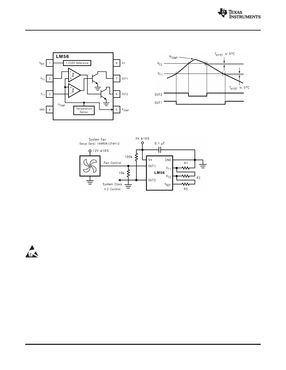
The LM56 is a precision low power thermostat. Two
2
Digital Outputs Support TTL Logic Levels
stable temperature trip points (V
T1
and V
T2
) are
Internal Temperature Sensor
generated
by
dividing
down
the
LM56
1.250V
2 Internal Comparators with Hysteresis
bandgap voltage reference using 3 external resistors.
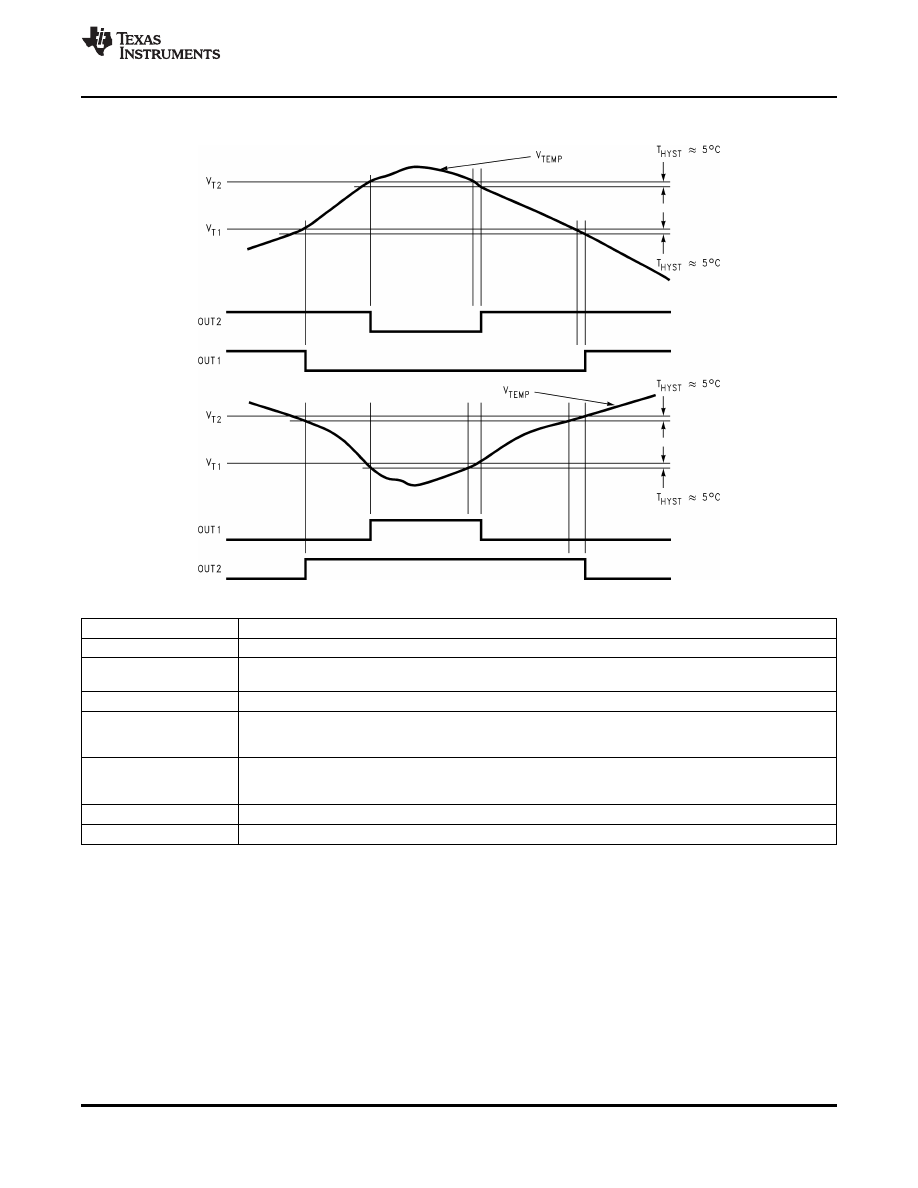
The LM56 has two digital outputs. OUT1 goes LOW
Internal Voltage Reference
when the temperature exceeds T1 and goes HIGH
Available in 8-pin SOIC and VSSOP Packages
when the the temperature goes below (T1-T
HYST
).
Similarly, OUT2 goes LOW when the temperature
APPLICATIONS
exceeds T2 and goes HIGH when the temperature
goes below (T2-T
HYST
). T
HYST
is an internally set 5 °C
Microprocessor Thermal Management
typical hysteresis.
Appliances
The LM56 is available in an 8-lead VSSOP surface
Portable Battery Powered 3.0V or 5V Systems
mount package and an 8-lead SOIC.
Fan Control
Industrial Process Control
HVAC Systems
Remote Temperature Sensing
Electronic System Protection
Table 1. Key Specifications
VALUE
UNIT
Power Supply Voltage
2.7V-10
V
Power Supply Current
230
μ
A (max)
V
REF
1.250
V ±1% (max)
Hysteresis Temperature
5
°C
(+6.20 mV/ °C x T) +
Internal Temperature Sensor Output Voltage
mV
395 mV
Table 2. Temperature Trip Point Accuracy
LM56BIM
LM56CIM
+25 °C
±2 °C (max)
±3 °C (max)
+25 °C to +85 °C
±2 °C (max)
±3 °C (max)
-
40 °C to +125 °C
±3 °C (max)
±4 °C (max)
1
Please be aware that an important notice concerning availability, standard warranty, and use in critical applications of
Texas Instruments semiconductor products and disclaimers thereto appears at the end of this data sheet.
2
All trademarks are the property of their respective owners.
PRODUCTION DATA information is current as of publication date.
Copyright © 2000-2013, Texas Instruments Incorporated
Products conform to specifications per the terms of the Texas
Instruments standard warranty. Production processing does not
necessarily include testing of all parameters.
SNIS120G - APRIL 2000 - REVISED FEBRUARY 2013
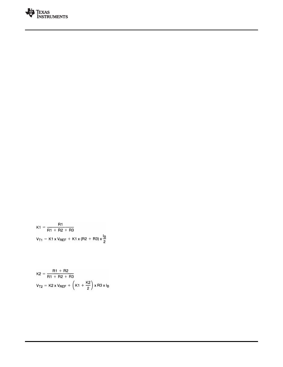
Simplified Block Diagram and Connection Diagram
Block Diagram
Typical Application
V
T1
= 1.250V x (R1)/(R1 + R2 + R3)
V
T2
= 1.250V x (R1 + R2)/(R1 + R2 + R3)
where:
(R1 + R2 + R3) = 27 k
Ω
and
V
T1 or T2
= [6.20 mV/ °C x T] + 395 mV therefore:
R1 = V
T1
/(1.25V) x 27 k
Ω
R2 = (V
T2
/(1.25V) x 27 k
Ω
)
-
R1
R3 = 27 k
Ω -
R1
-
R2
Figure 1. Microprocessor Thermal Management
These devices have limited built-in ESD protection. The leads should be shorted together or the device placed in conductive foam
during storage or handling to prevent electrostatic damage to the MOS gates.
2
Copyright © 2000-2013, Texas Instruments Incorporated
Product Folder Links:
SNIS120G - APRIL 2000 - REVISED FEBRUARY 2013
Absolute Maximum Ratings
(1)
Input Voltage
12V
Input Current at any pin
(2)
5 mA
Package Input Current
(2)
20 mA
Package Dissipation at T
A
= 25 °C
(3)
900 mW
Human Body Model - Pin 3 Only
800V
All other pins
1000V
ESD Susceptibility
(4)
Machine Model
125V
Storage Temperature
-
65 °C to + 150 °C
(1)
Absolute Maximum Ratings indicate limits beyond which damage to the device may occur. Operating Ratings indicate conditions for
which the device is functional, but do not guarantee specific performance limits. For guaranteed specifications and test conditions, see
the
The guaranteed specifications apply only for the test conditions listed. Some performance
characteristics may degrade when the device is not operated under the listed test conditions.
(2)
When the input voltage (V
I
) at any pin exceeds the power supply (V
I
< GND or V
I
> V
+
), the current at that pin should be limited to 5 mA.
The 20 mA maximum package input current rating limits the number of pins that can safely exceed the power supplies with an input
current of 5 mA to four.
(3)
The maximum power dissipation must be derated at elevated temperatures and is dictated by T
Jmax
(maximum junction temperature),
Θ
JA
(junction to ambient thermal resistance) and T
A
(ambient temperature). The maximum allowable power dissipation at any
temperature is P
D
= (T
Jmax
-T
A
)/
Θ
JA
or the number given in the Absolute Maximum Ratings, whichever is lower. For this device, T
Jmax
=
125 °C. For this device the typical thermal resistance (
Θ
JA
) of the different package types when board mounted follow:
(4)
The human body model is a 100 pF capacitor discharge through a 1.5 k
Ω
resistor into each pin. The machine model is a 200 pF
capacitor discharged directly into each pin.
Operating Ratings
(1) (2) (3)
Operating Temperature Range
T
MIN
≤
T
A
≤
T
MAX
LM56BIM, LM56CIM
-
40 °C
≤
T
A
≤
+125 °C
Positive Supply Voltage (V
+
)
+2.7V to +10V
Maximum V
OUT1
and V
OUT2
+10V
(1)
Absolute Maximum Ratings indicate limits beyond which damage to the device may occur. Operating Ratings indicate conditions for
which the device is functional, but do not guarantee specific performance limits. For guaranteed specifications and test conditions, see
the
The guaranteed specifications apply only for the test conditions listed. Some performance
characteristics may degrade when the device is not operated under the listed test conditions.
(2)
Soldering process must comply with Reflow Temperature Profile specifications. Refer to
(3)
Reflow temperature profiles are different for lead-free and non-lead-free packages.
Package Type
Θ
JA
D0008A
110 °C/W
DGK0008A
250 °C/W
Copyright © 2000-2013, Texas Instruments Incorporated
3
Product Folder Links:
SNIS120G - APRIL 2000 - REVISED FEBRUARY 2013
LM56 Electrical Characteristics
The following specifications apply for V
+
= 2.7 V
DC
, and V
REF
load current = 50
μ
A unless otherwise specified. Boldface limits
apply for T
A
= T
J
= T
MIN
to T
MAX
; all other limits T
A
= T
J
= 25 °C unless otherwise specified.
LM56BIM
LM56CIM
Symbol
Parameter
Conditions
Typical
(1)
Units (Limits)
Limits
(2)
Limits
(2)
Temperature Sensor
Trip Point Accuracy (Includes V
REF
,
±2
±3
°C (max)
Comparator Offset, and Temperature
+25 °C
≤
T
A
≤
+85 °C
±2
±3
°C (max)
Sensitivity errors)
-
40 °C
≤
T
A
≤
+125 °C
±3
±4
°C (max)
Trip Point Hysteresis
T
A
=
-
40 °C
4
3
3
°C (min)
6
6
°C (max)
T
A
= +25 °C
5
3.5
3.5
°C (min)
6.5
6.5
°C (max)
T
A
= +85 °C
6
4.5
4.5
°C (min)
7.5
7.5
°C (max)
T
A
= +125 °C
6
4
4
°C (min)
8
8
°C (max)
Internal Temperature Sensitivity
+6.20
mV/ °C
Temperature Sensitivity Error
±2
±3
°C (max)
±3
±4
°C (max)
Output Impedance
-
1
μ
A
≤
I
L
≤
+40
μ
A
1500
1500
Ω
(max)
Line Regulation
+3.0V
≤
V
+
≤
+10V,
-0.72/+0.3
-0.72/+0.3
mV/V (max)
+25 °C
≤
T
A
≤
+85 °C
6
6
+3.0V
≤
V
+
≤
+10V,
-1.14/+0.6
-1.14/+0.6
mV/V (max)
-
40 °C
≤
T
A
<25 °C
1
1
+2.7V
≤
V
+
≤
+3.3V
±2.3
±2.3
mV (max)
V
T1
and V
T2
Analog Inputs
I
BIAS
Analog Input Bias Current
150
300
300
nA (max)
V
IN
Analog Input Voltage Range
V
+
-
1
V
GND
V
V
OS
Comparator Offset
2
8
8
mV (max)
V
REF
Output
V
REF
V
REF
Nominal
1.250V
V
V
REF
Error
±1
±1
% (max)
±12.5
±12.5
mV (max)
Δ
V
REF
/
Δ
V
+
Line Regulation
+3.0V
≤
V
+
≤
+10V
0.13
0.25
0.25
mV/V (max)
+2.7V
≤
V
+
≤
+3.3V
0.15
1.1
1.1
mV (max)
Δ
V
REF
/
Δ
I
L
Load Regulation Sourcing
+30
μ
A
≤
I
L
≤
+50
μ
A
0.15
0.15
mV/
μ
A (max)
(1)
Typicals are at T
J
= T
A
= 25 °C and represent most likely parametric norm.
(2)
Limits are guaranteed to TI's AOQL (Average Outgoing Quality Level).
Symbol
Parameter
Conditions
Typical
(1)
Limits
(2)
Units (Limits)
V
+
Power Supply
I
S
Supply Current
V
+
= +10V
230
μ
A (max)
V
+
= +2.7V
230
μ
A (max)
Digital Outputs
I
OUT(1)
Logical 1 Output Leakage Current
V
+
= +5.0V
1
μ
A (max)
V
OUT(0)
Logical 0 Output Voltage
I
OUT
= +50
μ
A
0.4
V (max)
(1)
Typicals are at T
J
= T
A
= 25 °C and represent most likely parametric norm.
(2)
Limits are guaranteed to TI's AOQL (Average Outgoing Quality Level).
4
Copyright © 2000-2013, Texas Instruments Incorporated
Product Folder Links:
SNIS120G - APRIL 2000 - REVISED FEBRUARY 2013
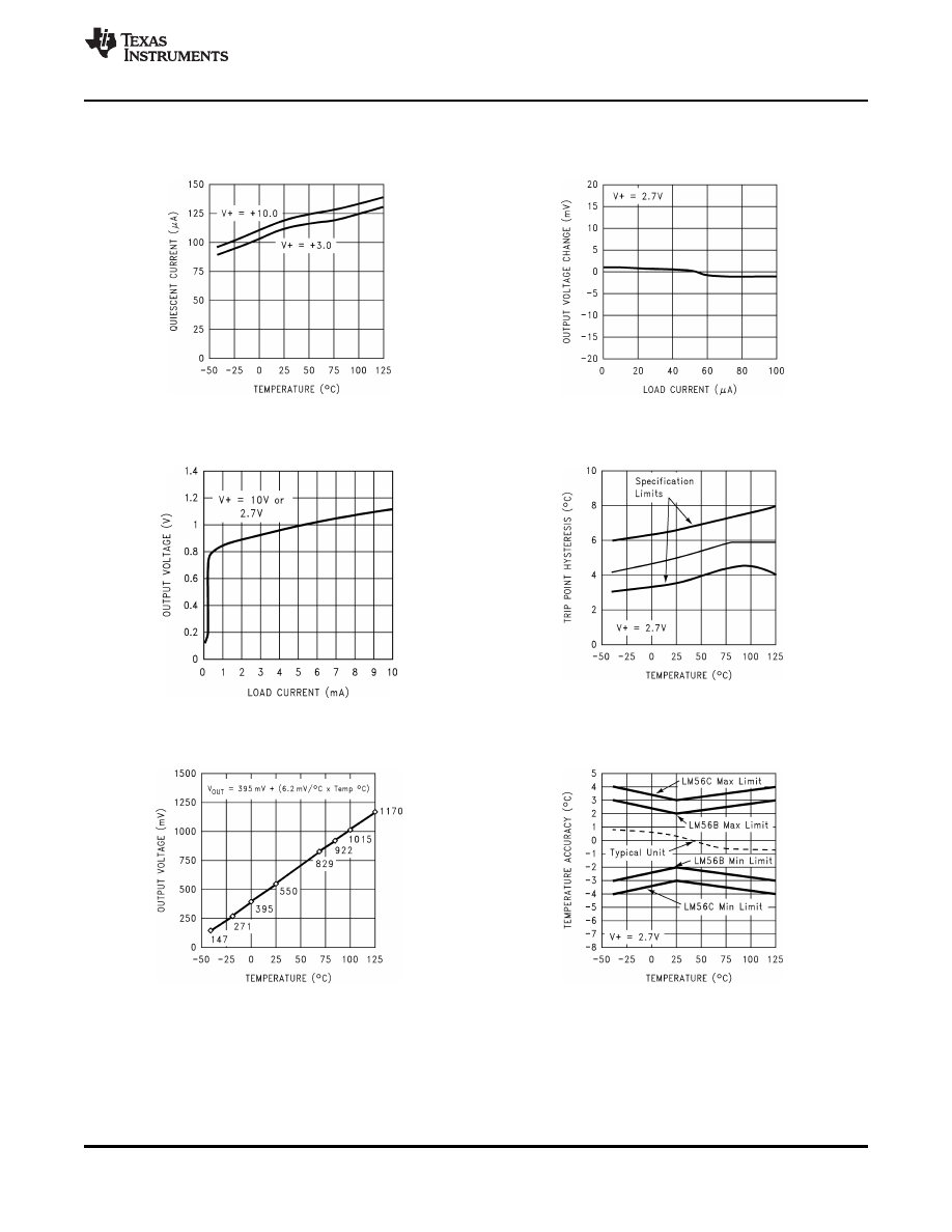
Typical Performance Characteristics
Quiescent Current
V
REF
Output Voltage
vs
vs
Temperature
Load Current
Figure 2.
Figure 3.
OUT1 and OUT2 Voltage Levels
Trip Point Hysteresis
vs
vs
Load Current
Temperature
Figure 4.
Figure 5.
Temperature Sensor Output Voltage
Temperature Sensor Output Accuracy
vs
vs
Temperature
Temperature
Figure 6.
Figure 7.
Copyright © 2000-2013, Texas Instruments Incorporated
5
Product Folder Links:
SNIS120G - APRIL 2000 - REVISED FEBRUARY 2013
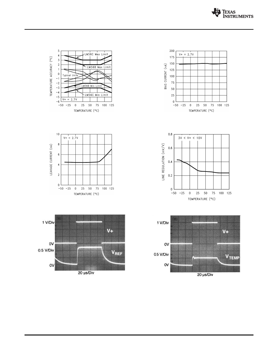
Typical Performance Characteristics (continued)
Trip Point Accuracy
Comparator Bias Current
vs
vs
Temperature
Temperature
Figure 8.
Figure 9.
OUT1 and OUT2 Leakage Current
V
TEMP
Output Line Regulation
vs
vs
Temperature
Temperature
Figure 10.
Figure 11.
V
REF
Start-Up Response
V
TEMP
Start-Up Response
Figure 12.
Figure 13.
6
Copyright © 2000-2013, Texas Instruments Incorporated
Product Folder Links:
SNIS120G - APRIL 2000 - REVISED FEBRUARY 2013
FUNCTIONAL DESCRIPTION
Pin Functions
V
+
This is the positive supply voltage pin. This pin should be bypassed with a 0.1 µF capacitor to ground.
GND
This is the ground pin.
V
REF
This is the 1.250V bandgap voltage reference output pin. In order to maintain trip point accuracy this pin
should source a 50 µA load.
V
TEMP
This is the temperature sensor output pin.
OUT1
This is an open collector digital output. OUT1 is active LOW. It goes LOW when the temperature is greater
than T
1
and goes HIGH when the temperature drops below T
1
- 5 °C. This output is not intended to directly
drive a fan motor.
OUT2
This is an open collector digital output. OUT2 is active LOW. It goes LOW when the temperature is greater
than the T
2
set point and goes HIGH when the temperature is less than T
2
- 5 °C. This output is not intended to
directly drive a fan motor.
V
T1
This is the input pin for the temperature trip point voltage for OUT1.
V
T2
This is the input pin for the low temperature trip point voltage for OUT2.
Copyright © 2000-2013, Texas Instruments Incorporated
7
Product Folder Links:
SNIS120G - APRIL 2000 - REVISED FEBRUARY 2013
V
T1
= 1.250V x (R1)/(R1 + R2 + R3)
V
T2
= 1.250V x (R1 + R2)/(R1 + R2 + R3)
where:
(R1 + R2 + R3) = 27 k
Ω
and
V
T1 or T2
= [6.20 mV/ °C x T] + 395 mV therefore:
R1 = V
T1
/(1.25V) x 27 k
Ω
R2 = (V
T2
/(1.25V) x 27 k)
Ω
-R1
R3 = 27 k
Ω -
R1
-
R2
Application Hints
LM56 TRIP POINT ACCURACY SPECIFICATION
For simplicity the following is an analysis of the trip point accuracy using the single output configuration shown in
with a set point of 82 °C.
Trip Point Error Voltage = V
TPE
,
Comparator Offset Error for V
T1E
Temperature Sensor Error = V
TSE
Reference Output Error = V
RE
Figure 14. Single Output Configuration
8
Copyright © 2000-2013, Texas Instruments Incorporated
Product Folder Links:
SNIS120G - APRIL 2000 - REVISED FEBRUARY 2013
1. V
TPE
= ±V
T1E
-
V
TSE
+ V
RE
Where:
2. V
T1E
= ±8 mV (max)
3. V
TSE
= (6.20 mV/ °C) x ( ±3 °C) = ±18.6 mV
4. V
RE
= 1.250V x ( ±0.01) R2/(R1 + R2)
Using Equations from
V
T1
= 1.25V x R2/(R1 + R2) = 6.20 mV/ °C)(82 °C) + 395 mV
Solving for R2/(R1 + R2) = 0.7227
then,
5. V
RE
= 1.250V x ( ±0.01) R2/(R1 + R2) = (0.0125) x (0.7227) = ±9.03 mV
The individual errors do not add algebraically because, the odds of all the errors being at their extremes are rare.
This is proven by the fact the specification for the trip point accuracy stated in the
for the temperature range of
-
40 °C to +125 °C, for example, is specified at ±3 °C for the LM56BIM. Note this trip
point error specification does not include any error introduced by the tolerance of the actual resistors used, nor
any error introduced by power supply variation.
If the resistors have a ±0.5% tolerance, an additional error of ±0.4 °C will be introduced. This error will increase to
±0.8 °C when both external resistors have a ±1% tolerance.
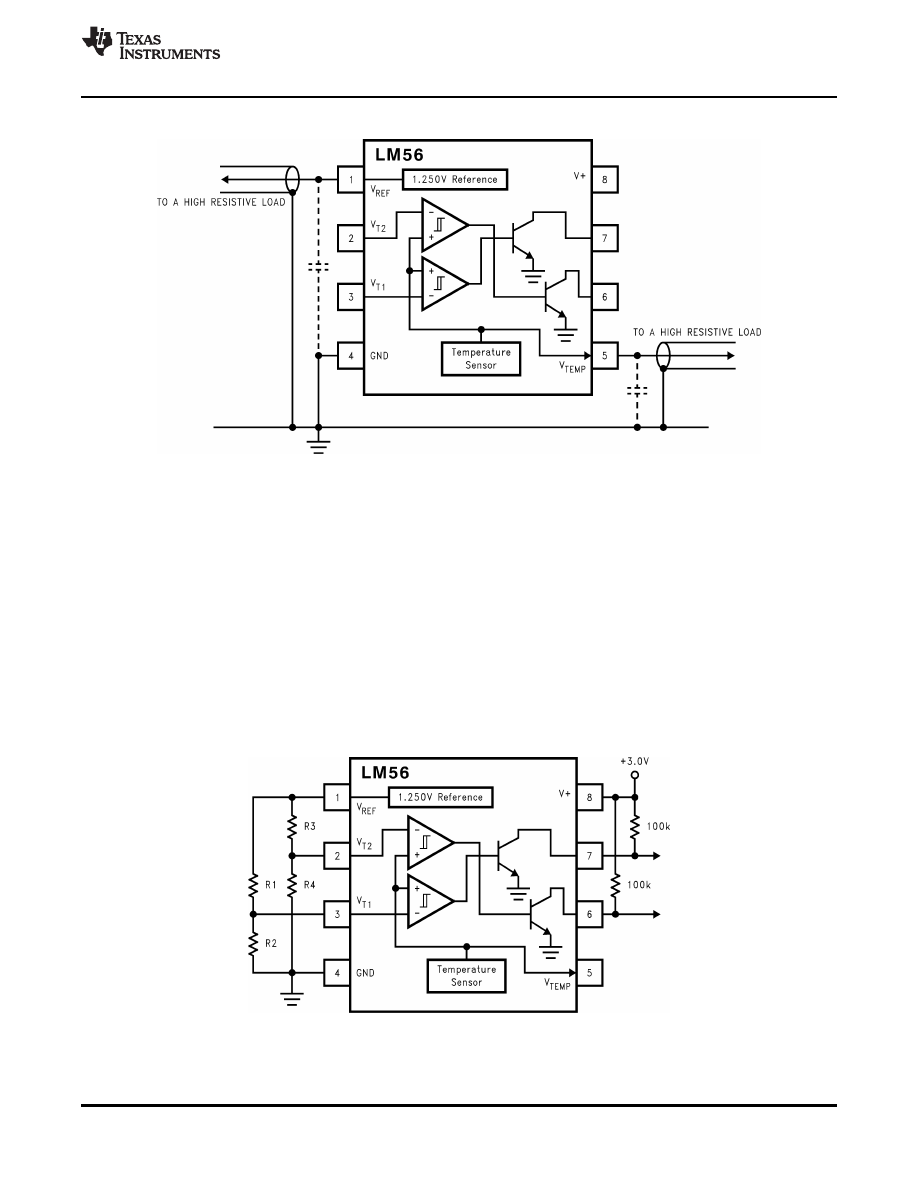
BIAS CURRENT EFFECT ON TRIP POINT ACCURACY
Bias current for the comparator inputs is 300 nA (max) each, over the specified temperature range and will not
introduce considerable error if the sum of the resistor values are kept to about 27 k
Ω
as shown in the typical
application of
This bias current of one comparator input will not flow if the temperature is well below the
trip point level. As the temperature approaches trip point level the bias current will start to flow into the resistor
network. When the temperature sensor output is equal to the trip point level the bias current will be 150 nA
(max). Once the temperature is well above the trip point level the bias current will be 300 nA (max). Therefore,
the first trip point will be affected by 150 nA of bias current. The leakage current is very small when the
comparator input transistor of the different pair is off (see
The effect of the bias current on the first trip point can be defined by the following equations:
(1)
where I
B
= 300 nA (the maximum specified error).
The effect of the bias current on the second trip point can be defined by the following equations:
(2)
where I
B
= 300 nA (the maximum specified error).
The closer the two trip points are to each other the more significant the error is. Worst case would be when V
T1
=
V
T2
= V
REF
/2.
Copyright © 2000-2013, Texas Instruments Incorporated
9
Product Folder Links:

SNIS120G - APRIL 2000 - REVISED FEBRUARY 2013
Figure 15. Simplified Schematic
MOUNTING CONSIDERATIONS
The majority of the temperature that the LM56 is measuring is the temperature of its leads. Therefore, when the
LM56 is placed on a printed circuit board, it is not sensing the temperature of the ambient air. It is actually
sensing the temperature difference of the air and the lands and printed circuit board that the leads are attached
to. The most accurate temperature sensing is obtained when the ambient temperature is equivalent to the
LM56's lead temperature.
As with any IC, the LM56 and accompanying wiring and circuits must be kept insulated and dry, to avoid leakage
and corrosion. This is especially true if the circuit operates at cold temperatures where condensation can occur.
Printed-circuit coatings are often used to ensure that moisture cannot corrode the LM56 or its connections.
10
Copyright © 2000-2013, Texas Instruments Incorporated
Product Folder Links:
SNIS120G - APRIL 2000 - REVISED FEBRUARY 2013
V
REF
AND V
TEMP
CAPACITIVE LOADING
Figure 16. Loading of V
REF
and V
TEMP
The LM56 V
REF
and V
TEMP
outputs handle capacitive loading well. Without any special precautions, these outputs
can drive any capacitive load as shown in
.
NOISY ENVIRONMENTS
Over the specified temperature range the LM56 V
TEMP
output has a maximum output impedance of 1500
Ω
. In an
extremely noisy environment it may be necessary to add some filtering to minimize noise pickup. It is
recommended that 0.1
μ
F be added from V
+
to GND to bypass the power supply voltage, as shown in
.
In a noisy environment it may be necessary to add a capacitor from the V
TEMP
output to ground. A 1
μ
F output
capacitor with the 1500
Ω
output impedance will form a 106 Hz lowpass filter. Since the thermal time constant of
the V
TEMP
output is much slower than the 9.4 ms time constant formed by the RC, the overall response time of
the V
TEMP
output will not be significantly affected. For much larger capacitors this additional time lag will increase
the overall response time of the LM56.
APPLICATIONS CIRCUITS
Figure 17. Reducing Errors Caused by Bias Current
Copyright © 2000-2013, Texas Instruments Incorporated
11
Product Folder Links:
SNIS120G - APRIL 2000 - REVISED FEBRUARY 2013
The circuit shown in
will reduce the effective bias current error for V
T2
as discussed in Section 3.0 to
be equivalent to the error term of V
T1
. For this circuit the effect of the bias current on the first trip point can be
defined by the following equations:
(3)
where I
B
= 300 nA (the maximum specified error).
Similarly, bias current affect on V
T2
can be defined by:
(4)
where I
B
= 300 nA (the maximum specified error).
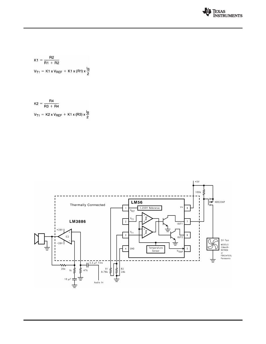
The current shown in
is a simple overtemperature detector for power devices. In this example, an
audio power amplifier IC is bolted to a heat sink and an LM56 Celsius temperature sensor is mounted on a PC
board that is bolted to the heat sink near the power amplifier. To ensure that the sensing element is at the same
temperature as the heat sink, the sensor's leads are mounted to pads that have feed throughs to the back side of
the PC board. Since the LM56 is sensing the temperature of the actual PC board the back side of the PC board
also has large ground plane to help conduct the heat to the device. The comparator's output goes low if the heat
sink temperature rises above a threshold set by R1, R2, and the voltage reference. This fault detection output
from the comparator now can be used to turn on a cooling fan. The circuit as shown in design to turn the fan on
when heat sink temperature exceeds about 80 °C, and to turn the fan off when the heat sink temperature falls
below approximately 75 °C.
Figure 18. Audio Power Amplifier Overtemperature Detector
12
Copyright © 2000-2013, Texas Instruments Incorporated
Product Folder Links:
SNIS120G - APRIL 2000 - REVISED FEBRUARY 2013
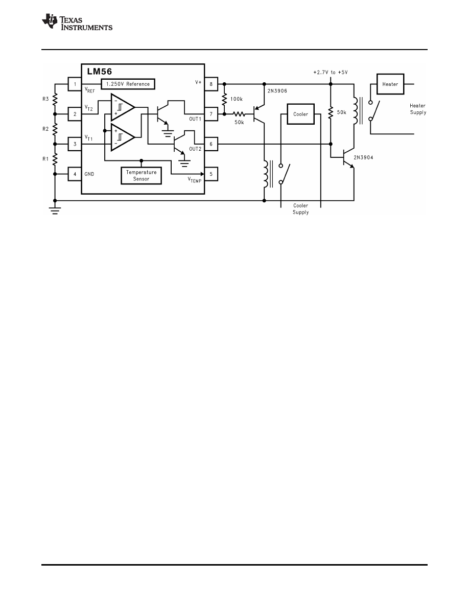
Figure 19. Simple Thermostat
Copyright © 2000-2013, Texas Instruments Incorporated
13
Product Folder Links:

SNIS120G - APRIL 2000 - REVISED FEBRUARY 2013
REVISION HISTORY
Changes from Revision F (February 2013) to Revision G
Page
Changed layout of National Data Sheet to TI format ..........................................................................................................
14
Copyright © 2000-2013, Texas Instruments Incorporated
Product Folder Links:
PACKAGE OPTION ADDENDUM
www.ti.com
27-Jul-2016
Addendum-Page 1
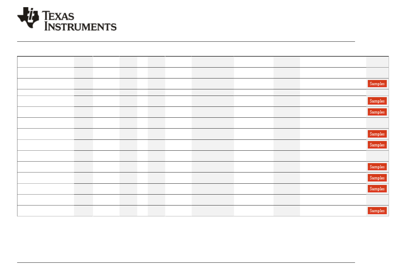
PACKAGING INFORMATION
Orderable Device
Status
(1)
Package Type Package
Drawing
Pins Package
Qty
Eco Plan
(2)
Lead/Ball Finish
(6)
MSL Peak Temp
(3)
Op Temp ( °C)
Device Marking
(4/5)
Samples
LM56BIM
NRND
SOIC
D
8
95
TBD
Call TI
Call TI
-40 to 125
LM56
BIM
LM56BIM/NOPB
ACTIVE
SOIC
D
8
95
Green (RoHS
& no Sb/Br)
CU SN
Level-1-260C-UNLIM
-40 to 125
LM56
BIM
LM56BIMM
NRND
VSSOP
DGK
8
1000
TBD
Call TI
Call TI
-40 to 125
T02B
LM56BIMM/NOPB
ACTIVE
VSSOP
DGK
8
1000
Green (RoHS
& no Sb/Br)
CU SN
Level-1-260C-UNLIM
-40 to 125
T02B
LM56BIMMX/NOPB
ACTIVE
VSSOP
DGK
8
3500
Green (RoHS
& no Sb/Br)
CU SN
Level-1-260C-UNLIM
-40 to 125
T02B
LM56BIMX
NRND
SOIC
D
8
2500
TBD
Call TI
Call TI
-40 to 125
LM56
BIM
LM56BIMX/NOPB
ACTIVE
SOIC
D
8
2500
Green (RoHS
& no Sb/Br)
CU SN
Level-1-260C-UNLIM
-40 to 125
LM56
BIM
LM56C MDC
ACTIVE
DIESALE
Y
0
165
Green (RoHS
& no Sb/Br)
Call TI
Level-1-NA-UNLIM
-40 to 85
LM56CIM
NRND
SOIC
D
8
95
TBD
Call TI
Call TI
-40 to 125
LM56
CIM
LM56CIM/NOPB
ACTIVE
SOIC
D
8
95
Green (RoHS
& no Sb/Br)
CU SN
Level-1-260C-UNLIM
-40 to 125
LM56
CIM
LM56CIMM/NOPB
ACTIVE
VSSOP
DGK
8
1000
Green (RoHS
& no Sb/Br)
CU SN
Level-1-260C-UNLIM
-40 to 125
T02C
LM56CIMMX/NOPB
ACTIVE
VSSOP
DGK
8
3500
Green (RoHS
& no Sb/Br)
CU SN
Level-1-260C-UNLIM
-40 to 125
T02C
LM56CIMX
NRND
SOIC
D
8
2500
TBD
Call TI
Call TI
-40 to 125
LM56
CIM
LM56CIMX/NOPB
ACTIVE
SOIC
D
8
2500
Green (RoHS
& no Sb/Br)
CU SN
Level-1-260C-UNLIM
-40 to 125
LM56
CIM
(1)
The marketing status values are defined as follows:
ACTIVE: Product device recommended for new designs.
LIFEBUY: TI has announced that the device will be discontinued, and a lifetime-buy period is in effect.
NRND: Not recommended for new designs. Device is in production to support existing customers, but TI does not recommend using this part in a new design.
PREVIEW: Device has been announced but is not in production. Samples may or may not be available.
OBSOLETE: TI has discontinued the production of the device.
PACKAGE OPTION ADDENDUM
www.ti.com
27-Jul-2016
Addendum-Page 2
(2)
Eco Plan - The planned eco-friendly classification: Pb-Free (RoHS), Pb-Free (RoHS Exempt), or Green (RoHS & no Sb/Br) - please check
for the latest availability
information and additional product content details.
TBD: The Pb-Free/Green conversion plan has not been defined.
Pb-Free (RoHS): TI's terms "Lead-Free" or "Pb-Free" mean semiconductor products that are compatible with the current RoHS requirements for all 6 substances, including the requirement that
lead not exceed 0.1% by weight in homogeneous materials. Where designed to be soldered at high temperatures, TI Pb-Free products are suitable for use in specified lead-free processes.
Pb-Free (RoHS Exempt): This component has a RoHS exemption for either 1) lead-based flip-chip solder bumps used between the die and package, or 2) lead-based die adhesive used between
the die and leadframe. The component is otherwise considered Pb-Free (RoHS compatible) as defined above.
Green (RoHS & no Sb/Br): TI defines "Green" to mean Pb-Free (RoHS compatible), and free of Bromine (Br) and Antimony (Sb) based flame retardants (Br or Sb do not exceed 0.1% by weight
in homogeneous material)
(3)
MSL, Peak Temp. - The Moisture Sensitivity Level rating according to the JEDEC industry standard classifications, and peak solder temperature.
(4)
There may be additional marking, which relates to the logo, the lot trace code information, or the environmental category on the device.
(5)
Multiple Device Markings will be inside parentheses. Only one Device Marking contained in parentheses and separated by a "~" will appear on a device. If a line is indented then it is a continuation
of the previous line and the two combined represent the entire Device Marking for that device.
(6)
Lead/Ball Finish - Orderable Devices may have multiple material finish options. Finish options are separated by a vertical ruled line. Lead/Ball Finish values may wrap to two lines if the finish
value exceeds the maximum column width.
Important Information and Disclaimer:The information provided on this page represents TI's knowledge and belief as of the date that it is provided. TI bases its knowledge and belief on information
provided by third parties, and makes no representation or warranty as to the accuracy of such information. Efforts are underway to better integrate information from third parties. TI has taken and
continues to take reasonable steps to provide representative and accurate information but may not have conducted destructive testing or chemical analysis on incoming materials and chemicals.
TI and TI suppliers consider certain information to be proprietary, and thus CAS numbers and other limited information may not be available for release.
In no event shall TI's liability arising out of such information exceed the total purchase price of the TI part(s) at issue in this document sold by TI to Customer on an annual basis.
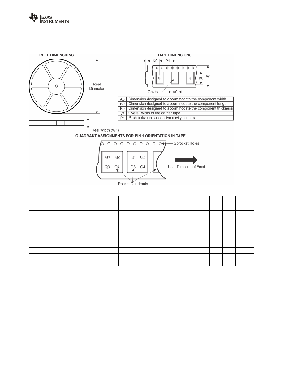
TAPE AND REEL INFORMATION
*All dimensions are nominal
Device
Package
Type
Package
Drawing
Pins
SPQ
Reel
Diameter
(mm)
Reel
Width
W1 (mm)
A0
(mm)
B0
(mm)
K0
(mm)
P1
(mm)
W
(mm)
Pin1
Quadrant
LM56BIMM
VSSOP
DGK
8
1000
178.0
12.4
5.3
3.4
1.4
8.0
12.0
Q1
LM56BIMM/NOPB
VSSOP
DGK
8
1000
178.0
12.4
5.3
3.4
1.4
8.0
12.0
Q1
LM56BIMMX/NOPB
VSSOP
DGK
8
3500
330.0
12.4
5.3
3.4
1.4
8.0
12.0
Q1
LM56BIMX
SOIC
D
8
2500
330.0
12.4
6.5
5.4
2.0
8.0
12.0
Q1
LM56BIMX/NOPB
SOIC
D
8
2500
330.0
12.4
6.5
5.4
2.0
8.0
12.0
Q1
LM56CIMM/NOPB
VSSOP
DGK
8
1000
178.0
12.4
5.3
3.4
1.4
8.0
12.0
Q1
LM56CIMMX/NOPB
VSSOP
DGK
8
3500
330.0
12.4
5.3
3.4
1.4
8.0
12.0
Q1
LM56CIMX
SOIC
D
8
2500
330.0
12.4
6.5
5.4
2.0
8.0
12.0
Q1
LM56CIMX/NOPB
SOIC
D
8
2500
330.0
12.4
6.5
5.4
2.0
8.0
12.0
Q1
PACKAGE MATERIALS INFORMATION
www.ti.com
7-May-2016
Pack Materials-Page 1
*All dimensions are nominal
Device
Package Type
Package Drawing
Pins
SPQ
Length (mm)
Width (mm)
Height (mm)
LM56BIMM
VSSOP
DGK
8
1000
210.0
185.0
35.0
LM56BIMM/NOPB
VSSOP
DGK
8
1000
210.0
185.0
35.0
LM56BIMMX/NOPB
VSSOP
DGK
8
3500
367.0
367.0
35.0
LM56BIMX
SOIC
D
8
2500
367.0
367.0
35.0
LM56BIMX/NOPB
SOIC
D
8
2500
367.0
367.0
35.0
LM56CIMM/NOPB
VSSOP
DGK
8
1000
210.0
185.0
35.0
LM56CIMMX/NOPB
VSSOP
DGK
8
3500
367.0
367.0
35.0
LM56CIMX
SOIC
D
8
2500
367.0
367.0
35.0
LM56CIMX/NOPB
SOIC
D
8
2500
367.0
367.0
35.0
PACKAGE MATERIALS INFORMATION
www.ti.com
7-May-2016
Pack Materials-Page 2

IMPORTANT NOTICE
Texas Instruments Incorporated and its subsidiaries (TI) reserve the right to make corrections, enhancements, improvements and other
changes to its semiconductor products and services per JESD46, latest issue, and to discontinue any product or service per JESD48, latest
issue. Buyers should obtain the latest relevant information before placing orders and should verify that such information is current and
complete. All semiconductor products (also referred to herein as components) are sold subject to TIs terms and conditions of sale
supplied at the time of order acknowledgment.
TI warrants performance of its components to the specifications applicable at the time of sale, in accordance with the warranty in TIs terms
and conditions of sale of semiconductor products. Testing and other quality control techniques are used to the extent TI deems necessary
to support this warranty. Except where mandated by applicable law, testing of all parameters of each component is not necessarily
performed.
TI assumes no liability for applications assistance or the design of Buyers products. Buyers are responsible for their products and
applications using TI components. To minimize the risks associated with Buyers products and applications, Buyers should provide
adequate design and operating safeguards.
TI does not warrant or represent that any license, either express or implied, is granted under any patent right, copyright, mask work right, or
other intellectual property right relating to any combination, machine, or process in which TI components or services are used. Information
published by TI regarding third-party products or services does not constitute a license to use such products or services or a warranty or
endorsement thereof. Use of such information may require a license from a third party under the patents or other intellectual property of the
third party, or a license from TI under the patents or other intellectual property of TI.
Reproduction of significant portions of TI information in TI data books or data sheets is permissible only if reproduction is without alteration
and is accompanied by all associated warranties, conditions, limitations, and notices. TI is not responsible or liable for such altered
documentation. Information of third parties may be subject to additional restrictions.
Resale of TI components or services with statements different from or beyond the parameters stated by TI for that component or service
voids all express and any implied warranties for the associated TI component or service and is an unfair and deceptive business practice.
TI is not responsible or liable for any such statements.
Buyer acknowledges and agrees that it is solely responsible for compliance with all legal, regulatory and safety-related requirements
concerning its products, and any use of TI components in its applications, notwithstanding any applications-related information or support
that may be provided by TI. Buyer represents and agrees that it has all the necessary expertise to create and implement safeguards which
anticipate dangerous consequences of failures, monitor failures and their consequences, lessen the likelihood of failures that might cause
harm and take appropriate remedial actions. Buyer will fully indemnify TI and its representatives against any damages arising out of the use
of any TI components in safety-critical applications.
In some cases, TI components may be promoted specifically to facilitate safety-related applications. With such components, TIs goal is to
help enable customers to design and create their own end-product solutions that meet applicable functional safety standards and
requirements. Nonetheless, such components are subject to these terms.
No TI components are authorized for use in FDA Class III (or similar life-critical medical equipment) unless authorized officers of the parties
have executed a special agreement specifically governing such use.
Only those TI components which TI has specifically designated as military grade or enhanced plastic are designed and intended for use in
military/aerospace applications or environments. Buyer acknowledges and agrees that any military or aerospace use of TI components
which have not been so designated is solely at the Buyer's risk, and that Buyer is solely responsible for compliance with all legal and
regulatory requirements in connection with such use.
TI has specifically designated certain components as meeting ISO/TS16949 requirements, mainly for automotive use. In any case of use of
non-designated products, TI will not be responsible for any failure to meet ISO/TS16949.
Products
Applications
Audio
Automotive and Transportation
Amplifiers
Communications and Telecom
Data Converters
Computers and Peripherals
DLP ® Products
Consumer Electronics
DSP
Energy and Lighting
Clocks and Timers
Industrial
Interface
Medical
Logic
Security
Power Mgmt
Space, Avionics and Defense
Microcontrollers
Video and Imaging
RFID
OMAP Applications Processors
TI E2E Community
Wireless Connectivity
Mailing Address: Texas Instruments, Post Office Box 655303, Dallas, Texas 75265
Copyright © 2016, Texas Instruments Incorporated
Document Outline

