| Secciones |
|---|
| Foros Electrónica |
|
|
| Boletines de correo |
 |
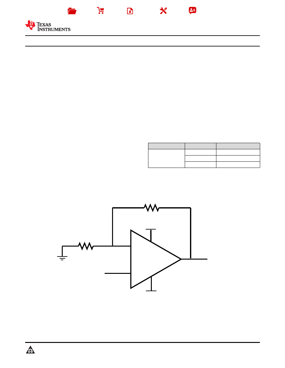
LM741
-
+
V-
V+
+V
supply
R1
V
input
Output
R2
-V
supply
SNOSC25D - MAY 1998 - REVISED OCTOBER 2015
LM741 Operational Amplifier
1 Features
3 Description
The LM741 series are general-purpose operational
1
Overload Protection on the Input and Output
amplifiers which feature improved performance over
No Latch-Up When the Common-Mode Range is
industry standards like the LM709. They are direct,
Exceeded
plug-in replacements for the 709C, LM201, MC1439,
and 748 in most applications.
2 Applications
The amplifiers offer many features which make their
Comparators
application nearly foolproof: overload protection on
the input and output, no latch-up when the common-
Multivibrators
mode range is exceeded, as well as freedom from
DC Amplifiers
oscillations.
Summing Amplifiers
The LM741C is identical to the LM741 and LM741A
Integrator or Differentiators
except that the LM741C has their performance
Active Filters
ensured over a 0 °C to +70 °C temperature range,
instead of
-55 °C to +125 °C.
Device
PART NUMBER
PACKAGE
BODY SIZE (NOM)
TO-99 (8)
9.08 mm × 9.08 mm
LM741
CDIP (8)
10.16 mm × 6.502 mm
PDIP (8)
9.81 mm × 6.35 mm
(1) For all available packages, see the orderable addendum at
the end of the data sheet.
Typical Application
1
An IMPORTANT NOTICE at the end of this data sheet addresses availability, warranty, changes, use in safety-critical applications,
intellectual property matters and other important disclaimers. PRODUCTION DATA.

SNOSC25D - MAY 1998 - REVISED OCTOBER 2015
Table of Contents
7.3
Feature Description...................................................
1
Features ..................................................................
7.4
Device Functional Modes..........................................
2
Applications ...........................................................
8
Application and Implementation ..........................
3
Description .............................................................
8.1
Application Information..............................................
4
Revision History.....................................................
8.2
Typical Application ...................................................
5
Pin Configuration and Functions .........................
9
Power Supply Recommendations ......................
6
Specifications.........................................................
10
Layout...................................................................
6.1
Absolute Maximum Ratings ......................................
10.1
Layout Guidelines .................................................
6.2
ESD Ratings..............................................................
10.2
Layout Example ....................................................
6.3
Recommended Operating Conditions .......................
11
Device and Documentation Support .................
6.4
Thermal Information ..................................................
11.1
Community Resources..........................................
6.5
Electrical Characteristics, LM741..............................
11.2
Trademarks ...........................................................
6.6
Electrical Characteristics, LM741A ...........................
11.3
Electrostatic Discharge Caution ............................
6.7
Electrical Characteristics, LM741C ...........................
11.4
Glossary ................................................................
7
Detailed Description ..............................................
12
Mechanical, Packaging, and Orderable
7.1
Overview ...................................................................
Information ...........................................................
7.2
Functional Block Diagram .........................................
4 Revision History
NOTE: Page numbers for previous revisions may differ from page numbers in the current version.
Changes from Revision C (October 2004) to Revision D
Page
Added Applications section, Pin Configuration and Functions section, ESD Ratings table, Feature Description
section, Device Functional Modes, Application and Implementation section, Power Supply Recommendations
section, Layout section, Device and Documentation Support section, and Mechanical, Packaging, and Orderable
Information section ................................................................................................................................................................
Removed NAD 10-Pin CLGA pinout .....................................................................................................................................
Removed obselete M (S0-8) package from the data sheet ...................................................................................................
Added recommended operating supply voltage spec ............................................................................................................
Added recommended operating temperature spec ................................................................................................................
Changes from Revision C (March 2013) to Revision D
Page
Added Applications section, Pin Configuration and Functions section, ESD Ratings table, Feature Description
section, Device Functional Modes, Application and Implementation section, Power Supply Recommendations
section, Layout section, Device and Documentation Support section, and Mechanical, Packaging, and Orderable
Information section ................................................................................................................................................................
Removed NAD 10-Pin CLGA pinout .....................................................................................................................................
Removed obselete M (S0-8) package from the data sheet ...................................................................................................
Added recommended operating supply voltage spec ............................................................................................................
Added recommended operating temperature spec ................................................................................................................
2
Copyright © 1998-2015, Texas Instruments Incorporated
Product Folder Links:
SNOSC25D - MAY 1998 - REVISED OCTOBER 2015
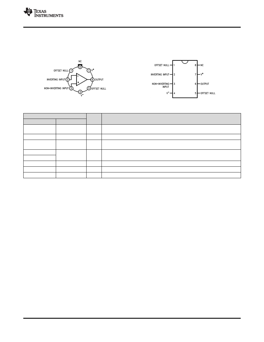
5 Pin Configuration and Functions
LMC Package
NAB Package
8-Pin TO-99
8-Pin CDIP or PDIP
Top View
Top View
LM741H is available per JM38510/10101
Pin Functions
PIN
I/O
DESCRIPTION
NAME
NO.
INVERTING
2
I
Inverting signal input
INPUT
NC
8
N/A
No Connect, should be left floating
NONINVERTING
3
I
Noninverting signal input
INPUT
OFFSET NULL
1, 5
I
Offset null pin used to eliminate the offset voltage and balance the input voltages.
OFFSET NULL
OUTPUT
6
O
Amplified signal output
V+
7
I
Positive supply voltage
V-
4
I
Negative supply voltage
Copyright © 1998-2015, Texas Instruments Incorporated
3
Product Folder Links:
SNOSC25D - MAY 1998 - REVISED OCTOBER 2015
6 Specifications
6.1 Absolute Maximum Ratings
over operating free-air temperature range (unless otherwise noted)
(1) (2) (3)
MIN
MAX
UNIT
LM741, LM741A
±22
Supply voltage
V
LM741C
±18
Power dissipation
(4)
500
mW
Differential input voltage
±30
V
Input voltage
(5)
±15
V
Output short circuit duration
Continuous
LM741, LM741A
-50
125
Operating temperature
°C
LM741C
0
70
LM741, LM741A
150
Junction temperature
°C
LM741C
100
PDIP package (10 seconds)
260
°C
Soldering information
CDIP or TO-99 package (10 seconds)
300
°C
Storage temperature, T
stg
-65
150
°C
(1)
Stresses beyond those listed under Absolute Maximum Ratings may cause permanent damage to the device. These are stress ratings
only, which do not imply functional operation of the device at these or any other conditions beyond those indicated under Recommended
Operating Conditions. Exposure to absolute-maximum-rated conditions for extended periods may affect device reliability.
(2)
For military specifications see RETS741X for LM741 and RETS741AX for LM741A.
(3)
If Military/Aerospace specified devices are required, please contact the TI Sales Office/Distributors for availability and specifications.
(4)
For operation at elevated temperatures, these devices must be derated based on thermal resistance, and T
j
max. (listed under Absolute
Maximum Ratings). T
j
= T
A
+ (
Θ
jA
P
D
).
(5)
For supply voltages less than ±15 V, the absolute maximum input voltage is equal to the supply voltage.
6.2 ESD Ratings
VALUE
UNIT
V
(ESD)
Electrostatic discharge
Human body model (HBM), per ANSI/ESDA/JEDEC JS-001
(1)
±400
V
(1)
Level listed above is the passing level per ANSI, ESDA, and JEDEC JS-001. JEDEC document JEP155 states that 500-V HBM allows
safe manufacturing with a standard ESD control process.
6.3 Recommended Operating Conditions
over operating free-air temperature range (unless otherwise noted)
MIN
NOM
MAX
UNIT
LM741, LM741A
±10
±15
±22
Supply voltage (VDD-GND)
V
LM741C
±10
±15
±18
LM741, LM741A
-55
125
Temperature
°C
LM741C
0
70
6.4 Thermal Information
LM741
THERMAL METRIC
(1)
LMC (TO-99)
NAB (CDIP)
P (PDIP)
UNIT
8 PINS
8 PINS
8 PINS
R
ΘJA
Junction-to-ambient thermal resistance
170
100
100
°C/W
R
ΘJC(top)
Junction-to-case (top) thermal resistance
25
°C/W
(1)
For more information about traditional and new thermal metrics, see the Semiconductor and IC Package Thermal Metrics application
report,
4
Copyright © 1998-2015, Texas Instruments Incorporated
Product Folder Links:
SNOSC25D - MAY 1998 - REVISED OCTOBER 2015
6.5 Electrical Characteristics, LM741
(1)
PARAMETER
TEST CONDITIONS
MIN
TYP
MAX
UNIT
T
A
= 25 °C
1
5
mV
Input offset voltage
R
S
≤ 10 kΩ
T
AMIN
≤ T
A
≤ T
AMAX
6
mV
Input offset voltage
T
A
= 25 °C, V
S
= ±20 V
±15
mV
adjustment range
T
A
= 25 °C
20
200
Input offset current
nA
T
AMIN
≤ T
A
≤ T
AMAX
85
500
T
A
= 25 °C
80
500
nA
Input bias current
T
AMIN
≤ T
A
≤ T
AMAX
1.5
μA
Input resistance
T
A
= 25 °C, V
S
= ±20 V
0.3
2
M
Ω
Input voltage range
T
AMIN
≤ T
A
≤ T
AMAX
±12
±13
V
T
A
= 25 °C
50
200
V
S
= ±15 V, V
O
= ±10 V, R
L
≥ 2
Large signal voltage gain
V/mV
k
Ω
T
AMIN
≤ T
A
≤ T
AMAX
25
R
L
≥ 10 kΩ
±12
±14
Output voltage swing
V
S
= ±15 V
V
R
L
≥ 2 kΩ
±10
±13
Output short circuit current
T
A
= 25 °C
25
mA
Common-mode rejection ratio
R
S
≤ 10 Ω, V
CM
= ±12 V, T
AMIN
≤ T
A
≤ T
AMAX
80
95
dB
Supply voltage rejection ratio
V
S
= ±20 V to V
S
= ±5 V, R
S
≤ 10 Ω, T
AMIN
≤ T
A
≤ T
AMAX
86
96
dB
Rise time
0.3
μs
Transient
T
A
= 25 °C, unity gain
response
Overshoot
5%
Slew rate
T
A
= 25 °C, unity gain
0.5
V/
μs
Supply current
T
A
= 25 °C
1.7
2.8
mA
T
A
= 25 °C
50
85
Power consumption
V
S
= ±15 V
T
A
= T
AMIN
60
100
mW
T
A
= T
AMAX
45
75
(1)
Unless otherwise specified, these specifications apply for V
S
= ±15 V,
-55 °C ≤ T
A
≤ +125 °C (LM741/LM741A). For the
LM741C/LM741E, these specifications are limited to 0 °C
≤ T
A
≤ +70 °C.
6.6 Electrical Characteristics, LM741A
(1)
PARAMETER
TEST CONDITIONS
MIN
TYP
MAX
UNIT
T
A
= 25 °C
0.8
3
mV
Input offset voltage
R
S
≤ 50 Ω
T
AMIN
≤ T
A
≤ T
AMAX
4
mV
Average input offset voltage
15
μV/ °C
drift
Input offset voltage
T
A
= 25 °C, V
S
= ±20 V
±10
mV
adjustment range
T
A
= 25 °C
3
30
Input offset current
nA
T
AMIN
≤ T
A
≤ T
AMAX
70
Average input offset
0.5
nA/ °C
current drift
T
A
= 25 °C
30
80
nA
Input bias current
T
AMIN
≤ T
A
≤ T
AMAX
0.21
μA
T
A
= 25 °C, V
S
= ±20 V
1
6
Input resistance
M
Ω
T
AMIN
≤ T
A
≤ T
AMAX
, V
S
= ±20 V
0.5
T
A
= 25 °C
50
V
S
= ±20 V, V
O
= ±15 V, R
L
≥ 2
k
Ω
Large signal voltage gain
T
AMIN
≤ T
A
≤ T
AMAX
32
V/mV
V
S
= ±5 V, V
O
= ±2 V, R
L
≥ 2 kΩ, T
AMIN
≤ T
A
≤ T
AMAX
10
(1)
Unless otherwise specified, these specifications apply for V
S
= ±15 V,
-55 °C ≤ T
A
≤ +125 °C (LM741/LM741A). For the
LM741C/LM741E, these specifications are limited to 0 °C
≤ T
A
≤ +70 °C.
Copyright © 1998-2015, Texas Instruments Incorporated
5
Product Folder Links:
SNOSC25D - MAY 1998 - REVISED OCTOBER 2015
Electrical Characteristics,
(continued)
PARAMETER
TEST CONDITIONS
MIN
TYP
MAX
UNIT
R
L
≥ 10 kΩ
±16
Output voltage swing
V
S
= ±20 V
V
R
L
≥ 2 kΩ
±15
T
A
= 25 °C
10
25
35
Output short circuit current
mA
T
AMIN
≤ T
A
≤ T
AMAX
10
40
Common-mode rejection ratio R
S
≤ 50 Ω, V
CM
= ±12 V, T
AMIN
≤ T
A
≤ T
AMAX
80
95
dB
Supply voltage rejection ratio
V
S
= ±20 V to V
S
= ±5 V, R
S
≤ 50 Ω, T
AMIN
≤ T
A
≤ T
AMAX
86
96
dB
Rise time
0.25
0.8
μs
Transient
T
A
= 25 °C, unity gain
response
Overshoot
6%
20%
Bandwidth
(2)
T
A
= 25 °C
0.437
1.5
MHz
Slew rate
T
A
= 25 °C, unity gain
0.3
0.7
V/
μs
T
A
= 25 °C
80
150
Power consumption
V
S
= ±20 V
T
A
= T
AMIN
165
mW
T
A
= T
AMAX
135
(2)
Calculated value from: BW (MHz) = 0.35/Rise Time (
μs).
6.7 Electrical Characteristics, LM741C
(1)
PARAMETER
TEST CONDITIONS
MIN
TYP
MAX
UNIT
T
A
= 25 °C
2
6
mV
Input offset voltage
R
S
≤ 10 kΩ
T
AMIN
≤ T
A
≤ T
AMAX
7.5
mV
Input offset voltage
T
A
= 25 °C, V
S
= ±20 V
±15
mV
adjustment range
T
A
= 25 °C
20
200
Input offset current
nA
T
AMIN
≤ T
A
≤ T
AMAX
300
T
A
= 25 °C
80
500
nA
Input bias current
T
AMIN
≤ T
A
≤ T
AMAX
0.8
μA
Input resistance
T
A
= 25 °C, V
S
= ±20 V
0.3
2
M
Ω
Input voltage range
T
A
= 25 °C
±12
±13
V
T
A
= 25 °C
20
200
V
S
= ±15 V, V
O
= ±10 V, R
L
Large signal voltage gain
V/mV
≥ 2 kΩ
T
AMIN
≤ T
A
≤ T
AMAX
15
R
L
≥ 10 kΩ
±12
±14
Output voltage swing
V
S
= ±15 V
V
R
L
≥ 2 kΩ
±10
±13
Output short circuit current
T
A
= 25 °C
25
mA
Common-mode rejection ratio
R
S
≤ 10 kΩ, V
CM
= ±12 V, T
AMIN
≤ T
A
≤ T
AMAX
70
90
dB
Supply voltage rejection ratio
V
S
= ±20 V to V
S
= ±5 V, R
S
≤ 10 Ω, T
AMIN
≤ T
A
≤ T
AMAX
77
96
dB
Rise time
0.3
μs
Transient response
T
A
= 25 °C, Unity Gain
Overshoot
5%
Slew rate
T
A
= 25 °C, Unity Gain
0.5
V/
μs
Supply current
T
A
= 25 °C
1.7
2.8
mA
Power consumption
V
S
= ±15 V, T
A
= 25 °C
50
85
mW
(1)
Unless otherwise specified, these specifications apply for V
S
= ±15 V,
-55 °C ≤ T
A
≤ +125 °C (LM741/LM741A). For the
LM741C/LM741E, these specifications are limited to 0 °C
≤ T
A
≤ +70 °C.
6
Copyright © 1998-2015, Texas Instruments Incorporated
Product Folder Links:
SNOSC25D - MAY 1998 - REVISED OCTOBER 2015
7 Detailed Description
7.1 Overview
The LM74 devices are general-purpose operational amplifiers which feature improved performance over industry
standards like the LM709. It is intended for a wide range of analog applications. The high gain and wide range of
operating voltage provide superior performance in integrator, summing amplifier, and general feedback
applications. The LM741 can operate with a single or dual power supply voltage. The LM741 devices are direct,
plug-in replacements for the 709C, LM201, MC1439, and 748 in most applications.
7.2 Functional Block Diagram
7.3 Feature Description
7.3.1 Overload Protection
The LM741 features overload protection circuitry on the input and output. This prevents possible circuit damage
to the device.
7.3.2 Latch-up Prevention
The LM741 is designed so that there is no latch-up occurrence when the common-mode range is exceeded. This
allows the device to function properly without having to power cycle the device.
7.3.3 Pin-to-Pin Capability
The LM741 is pin-to-pin direct replacements for the LM709C, LM201, MC1439, and LM748 in most applications.
Direct replacement capabilities allows flexibility in design for replacing obsolete parts.
Copyright © 1998-2015, Texas Instruments Incorporated
7
Product Folder Links:

SNOSC25D - MAY 1998 - REVISED OCTOBER 2015
7.4 Device Functional Modes
7.4.1 Open-Loop Amplifier
The LM741 can be operated in an open-loop configuration. The magnitude of the open-loop gain is typically large
thus for a small difference between the noninverting and inverting input terminals, the amplifier output will be
driven near the supply voltage. Without negative feedback, the LM741 can act as a comparator. If the inverting
input is held at 0 V, and the input voltage applied to the noninverting input is positive, the output will be positive.
If the input voltage applied to the noninverting input is negative, the output will be negative.
7.4.2 Closed-Loop Amplifier
In a closed-loop configuration, negative feedback is used by applying a portion of the output voltage to the
inverting input. Unlike the open-loop configuration, closed loop feedback reduces the gain of the circuit. The
overall gain and response of the circuit is determined by the feedback network rather than the operational
amplifier characteristics. The response of the operational amplifier circuit is characterized by the transfer function.
8
Copyright © 1998-2015, Texas Instruments Incorporated
Product Folder Links:
LM741
-
+
V-
V+
+V
supply
R1 = 4.7k
V
input
Output
R2 = 4.7k
-V
supply
SNOSC25D - MAY 1998 - REVISED OCTOBER 2015
8 Application and Implementation
NOTE
Information in the following applications sections is not part of the TI component
specification, and TI does not warrant its accuracy or completeness. TIs customers are
responsible for determining suitability of components for their purposes. Customers should
validate and test their design implementation to confirm system functionality.
8.1 Application Information
The LM741 is a general-purpose amplifier than can be used in a variety of applications and configurations. One
common configuration is in a noninverting amplifier configuration. In this configuration, the output signal is in
phase with the input (not inverted as in the inverting amplifier configuration), the input impedance of the amplifier
is high, and the output impedance is low. The characteristics of the input and output impedance is beneficial for
applications that require isolation between the input and output. No significant loading will occur from the
previous stage before the amplifier. The gain of the system is set accordingly so the output signal is a factor
larger than the input signal.
8.2 Typical Application
Figure 1. LM741 Noninverting Amplifier Circuit
8.2.1 Design Requirements
As shown in
the signal is applied to the noninverting input of the LM741. The gain of the system is
determined by the feedback resistor and input resistor connected to the inverting input. The gain can be
calculated by
:
Gain = 1 + (R2/R1)
(1)
The gain is set to 2 for this application. R1 and R2 are 4.7-k resistors with 5% tolerance.
8.2.2 Detailed Design Procedure
The LM741 can be operated in either single supply or dual supply. This application is configured for dual supply
with the supply rails at ±15 V. The input signal is connected to a function generator. A 1-Vpp, 10-kHz sine wave
was used as the signal input. 5% tolerance resistors were used, but if the application requires an accurate gain
response, use 1% tolerance resistors.
Copyright © 1998-2015, Texas Instruments Incorporated
9
Product Folder Links:
SNOSC25D - MAY 1998 - REVISED OCTOBER 2015
Typical Application (continued)
8.2.3 Application Curve
The waveforms in
show the input and output signals of the LM741 non-inverting amplifier circuit. The
blue waveform (top) shows the input signal, while the red waveform (bottom) shows the output signal. The input
signal is 1.06 Vpp and the output signal is 1.94 Vpp. With the 4.7-k
Ω resistors, the theoretical gain of the system
is 2. Due to the 5% tolerance, the gain of the system including the tolerance is 1.992. The gain of the system
when measured from the mean amplitude values on the oscilloscope was 1.83.
Figure 2. Waveforms for LM741 Noninverting Amplifier Circuit
9 Power Supply Recommendations
For proper operation, the power supplies must be properly decoupled. For decoupling the supply lines, a 0.1- µF
capacitor is recommended and should be placed as close as possible to the LM741 power supply pins.
10
Copyright © 1998-2015, Texas Instruments Incorporated
Product Folder Links:
SNOSC25D - MAY 1998 - REVISED OCTOBER 2015
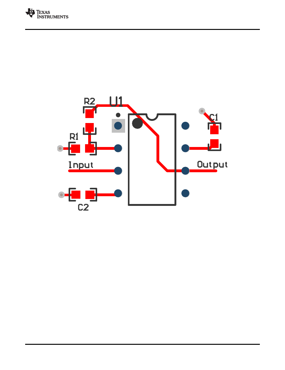
10 Layout
10.1 Layout Guidelines
As with most amplifiers, take care with lead dress, component placement, and supply decoupling in order to
ensure stability. For example, resistors from the output to an input should be placed with the body close to the
input to minimize pick-up and maximize the frequency of the feedback pole by minimizing the capacitance from
the input to ground. As shown in
, the feedback resistors and the decoupling capacitors are located close
to the device to ensure maximum stability and noise performance of the system.
10.2 Layout Example
Figure 3. LM741 Layout
Copyright © 1998-2015, Texas Instruments Incorporated
11
Product Folder Links:
SNOSC25D - MAY 1998 - REVISED OCTOBER 2015
11 Device and Documentation Support
11.1 Community Resources
The following links connect to TI community resources. Linked contents are provided "AS IS" by the respective
contributors. They do not constitute TI specifications and do not necessarily reflect TI's views; see TI's
TI's Engineer-to-Engineer (E2E) Community. Created to foster collaboration
among engineers. At e2e.ti.com, you can ask questions, share knowledge, explore ideas and help
solve problems with fellow engineers.
TI's Design Support Quickly find helpful E2E forums along with design support tools and
contact information for technical support.
11.2 Trademarks
E2E is a trademark of Texas Instruments.
All other trademarks are the property of their respective owners.
11.3 Electrostatic Discharge Caution
These devices have limited built-in ESD protection. The leads should be shorted together or the device placed in conductive foam
during storage or handling to prevent electrostatic damage to the MOS gates.
11.4 Glossary
TI Glossary.
This glossary lists and explains terms, acronyms, and definitions.
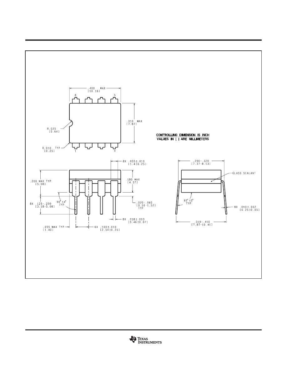
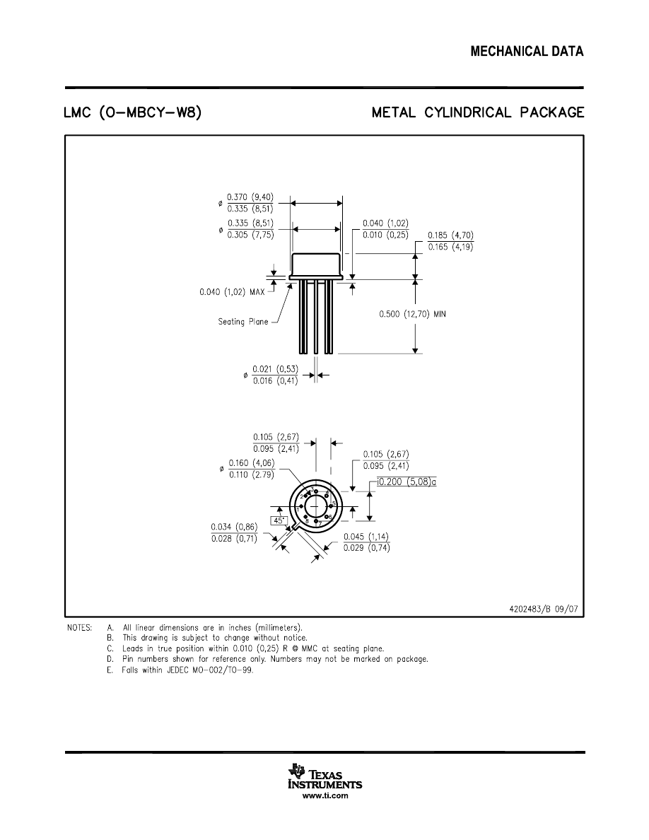
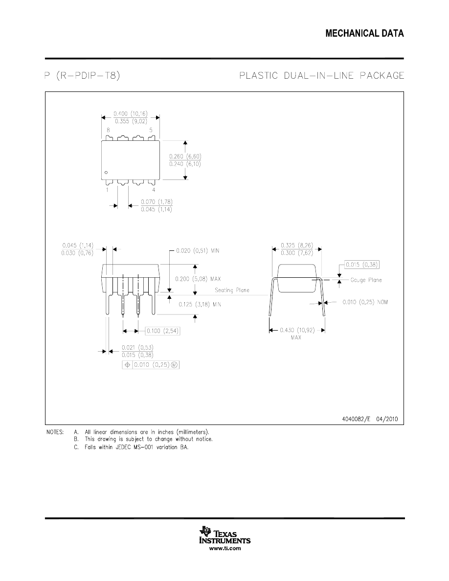
12 Mechanical, Packaging, and Orderable Information
The following pages include mechanical, packaging, and orderable information. This information is the most
current data available for the designated devices. This data is subject to change without notice and revision of
this document. For browser-based versions of this data sheet, refer to the left-hand navigation.
12
Copyright © 1998-2015, Texas Instruments Incorporated
Product Folder Links:
PACKAGE OPTION ADDENDUM
www.ti.com
5-May-2016
Addendum-Page 1
PACKAGING INFORMATION
Orderable Device
Status
(1)
Package Type Package
Drawing
Pins Package
Qty
Eco Plan
(2)
Lead/Ball Finish
(6)
MSL Peak Temp
(3)
Op Temp ( °C)
Device Marking
(4/5)
Samples
LM741 MD8
ACTIVE
DIESALE
Y
0
400
Green (RoHS
& no Sb/Br)
Call TI
Level-1-NA-UNLIM
LM741C-MWC
ACTIVE
WAFERSALE
YS
0
1
Green (RoHS
& no Sb/Br)
Call TI
Level-1-NA-UNLIM
LM741CH
ACTIVE
TO-99
LMC
8
500
TBD
Call TI
Call TI
0 to 70
( LM741CH ~
LM741CH)
LM741CH/NOPB
ACTIVE
TO-99
LMC
8
500
Green (RoHS
& no Sb/Br)
Call TI
Level-1-NA-UNLIM
0 to 70
( LM741CH ~
LM741CH)
LM741CN/NOPB
ACTIVE
PDIP
P
8
40
Green (RoHS
& no Sb/Br)
CU SN
Level-1-NA-UNLIM
0 to 70
LM
741CN
LM741H
ACTIVE
TO-99
LMC
8
500
TBD
Call TI
Call TI
-55 to 125
( LM741H ~ LM741H)
LM741H/NOPB
ACTIVE
TO-99
LMC
8
500
Green (RoHS
& no Sb/Br)
Call TI
Level-1-NA-UNLIM
-55 to 125
( LM741H ~ LM741H)
LM741J
ACTIVE
CDIP
NAB
8
40
TBD
Call TI
Call TI
-55 to 125
LM741J
U5B7741312
ACTIVE
TO-99
LMC
8
500
TBD
Call TI
Call TI
-55 to 125
( LM741H ~ LM741H)
U5B7741393
ACTIVE
TO-99
LMC
8
500
TBD
Call TI
Call TI
0 to 70
( LM741CH ~
LM741CH)
U9T7741393
OBSOLETE
PDIP
P
8
TBD
Call TI
Call TI
0 to 70
LM
741CN
(1)
The marketing status values are defined as follows:
ACTIVE: Product device recommended for new designs.
LIFEBUY: TI has announced that the device will be discontinued, and a lifetime-buy period is in effect.
NRND: Not recommended for new designs. Device is in production to support existing customers, but TI does not recommend using this part in a new design.
PREVIEW: Device has been announced but is not in production. Samples may or may not be available.
OBSOLETE: TI has discontinued the production of the device.
(2)
Eco Plan - The planned eco-friendly classification: Pb-Free (RoHS), Pb-Free (RoHS Exempt), or Green (RoHS & no Sb/Br) - please check
for the latest availability
information and additional product content details.
TBD: The Pb-Free/Green conversion plan has not been defined.
Pb-Free (RoHS): TI's terms "Lead-Free" or "Pb-Free" mean semiconductor products that are compatible with the current RoHS requirements for all 6 substances, including the requirement that
lead not exceed 0.1% by weight in homogeneous materials. Where designed to be soldered at high temperatures, TI Pb-Free products are suitable for use in specified lead-free processes.
Pb-Free (RoHS Exempt): This component has a RoHS exemption for either 1) lead-based flip-chip solder bumps used between the die and package, or 2) lead-based die adhesive used between
the die and leadframe. The component is otherwise considered Pb-Free (RoHS compatible) as defined above.
PACKAGE OPTION ADDENDUM
www.ti.com
5-May-2016
Addendum-Page 2
Green (RoHS & no Sb/Br): TI defines "Green" to mean Pb-Free (RoHS compatible), and free of Bromine (Br) and Antimony (Sb) based flame retardants (Br or Sb do not exceed 0.1% by weight
in homogeneous material)
(3)
MSL, Peak Temp. - The Moisture Sensitivity Level rating according to the JEDEC industry standard classifications, and peak solder temperature.
(4)
There may be additional marking, which relates to the logo, the lot trace code information, or the environmental category on the device.
(5)
Multiple Device Markings will be inside parentheses. Only one Device Marking contained in parentheses and separated by a "~" will appear on a device. If a line is indented then it is a continuation
of the previous line and the two combined represent the entire Device Marking for that device.
(6)
Lead/Ball Finish - Orderable Devices may have multiple material finish options. Finish options are separated by a vertical ruled line. Lead/Ball Finish values may wrap to two lines if the finish
value exceeds the maximum column width.
Important Information and Disclaimer:The information provided on this page represents TI's knowledge and belief as of the date that it is provided. TI bases its knowledge and belief on information
provided by third parties, and makes no representation or warranty as to the accuracy of such information. Efforts are underway to better integrate information from third parties. TI has taken and
continues to take reasonable steps to provide representative and accurate information but may not have conducted destructive testing or chemical analysis on incoming materials and chemicals.
TI and TI suppliers consider certain information to be proprietary, and thus CAS numbers and other limited information may not be available for release.
In no event shall TI's liability arising out of such information exceed the total purchase price of the TI part(s) at issue in this document sold by TI to Customer on an annual basis.
MECHANICAL DATA
NAB0008A
www.ti.com
J08A (Rev M)

IMPORTANT NOTICE
Texas Instruments Incorporated and its subsidiaries (TI) reserve the right to make corrections, enhancements, improvements and other
changes to its semiconductor products and services per JESD46, latest issue, and to discontinue any product or service per JESD48, latest
issue. Buyers should obtain the latest relevant information before placing orders and should verify that such information is current and
complete. All semiconductor products (also referred to herein as components) are sold subject to TIs terms and conditions of sale
supplied at the time of order acknowledgment.
TI warrants performance of its components to the specifications applicable at the time of sale, in accordance with the warranty in TIs terms
and conditions of sale of semiconductor products. Testing and other quality control techniques are used to the extent TI deems necessary
to support this warranty. Except where mandated by applicable law, testing of all parameters of each component is not necessarily
performed.
TI assumes no liability for applications assistance or the design of Buyers products. Buyers are responsible for their products and
applications using TI components. To minimize the risks associated with Buyers products and applications, Buyers should provide
adequate design and operating safeguards.
TI does not warrant or represent that any license, either express or implied, is granted under any patent right, copyright, mask work right, or
other intellectual property right relating to any combination, machine, or process in which TI components or services are used. Information
published by TI regarding third-party products or services does not constitute a license to use such products or services or a warranty or
endorsement thereof. Use of such information may require a license from a third party under the patents or other intellectual property of the
third party, or a license from TI under the patents or other intellectual property of TI.
Reproduction of significant portions of TI information in TI data books or data sheets is permissible only if reproduction is without alteration
and is accompanied by all associated warranties, conditions, limitations, and notices. TI is not responsible or liable for such altered
documentation. Information of third parties may be subject to additional restrictions.
Resale of TI components or services with statements different from or beyond the parameters stated by TI for that component or service
voids all express and any implied warranties for the associated TI component or service and is an unfair and deceptive business practice.
TI is not responsible or liable for any such statements.
Buyer acknowledges and agrees that it is solely responsible for compliance with all legal, regulatory and safety-related requirements
concerning its products, and any use of TI components in its applications, notwithstanding any applications-related information or support
that may be provided by TI. Buyer represents and agrees that it has all the necessary expertise to create and implement safeguards which
anticipate dangerous consequences of failures, monitor failures and their consequences, lessen the likelihood of failures that might cause
harm and take appropriate remedial actions. Buyer will fully indemnify TI and its representatives against any damages arising out of the use
of any TI components in safety-critical applications.
In some cases, TI components may be promoted specifically to facilitate safety-related applications. With such components, TIs goal is to
help enable customers to design and create their own end-product solutions that meet applicable functional safety standards and
requirements. Nonetheless, such components are subject to these terms.
No TI components are authorized for use in FDA Class III (or similar life-critical medical equipment) unless authorized officers of the parties
have executed a special agreement specifically governing such use.
Only those TI components which TI has specifically designated as military grade or enhanced plastic are designed and intended for use in
military/aerospace applications or environments. Buyer acknowledges and agrees that any military or aerospace use of TI components
which have not been so designated is solely at the Buyer's risk, and that Buyer is solely responsible for compliance with all legal and
regulatory requirements in connection with such use.
TI has specifically designated certain components as meeting ISO/TS16949 requirements, mainly for automotive use. In any case of use of
non-designated products, TI will not be responsible for any failure to meet ISO/TS16949.
Products
Applications
Audio
Automotive and Transportation
Amplifiers
Communications and Telecom
Data Converters
Computers and Peripherals
DLP ® Products
Consumer Electronics
DSP
Energy and Lighting
Clocks and Timers
Industrial
Interface
Medical
Logic
Security
Power Mgmt
Space, Avionics and Defense
Microcontrollers
Video and Imaging
RFID
OMAP Applications Processors
TI E2E Community
Wireless Connectivity
Mailing Address: Texas Instruments, Post Office Box 655303, Dallas, Texas 75265
Copyright © 2016, Texas Instruments Incorporated
Document Outline

