| Secciones |
|---|
| Foros Electrónica |
|
|
| Boletines de correo |
 |
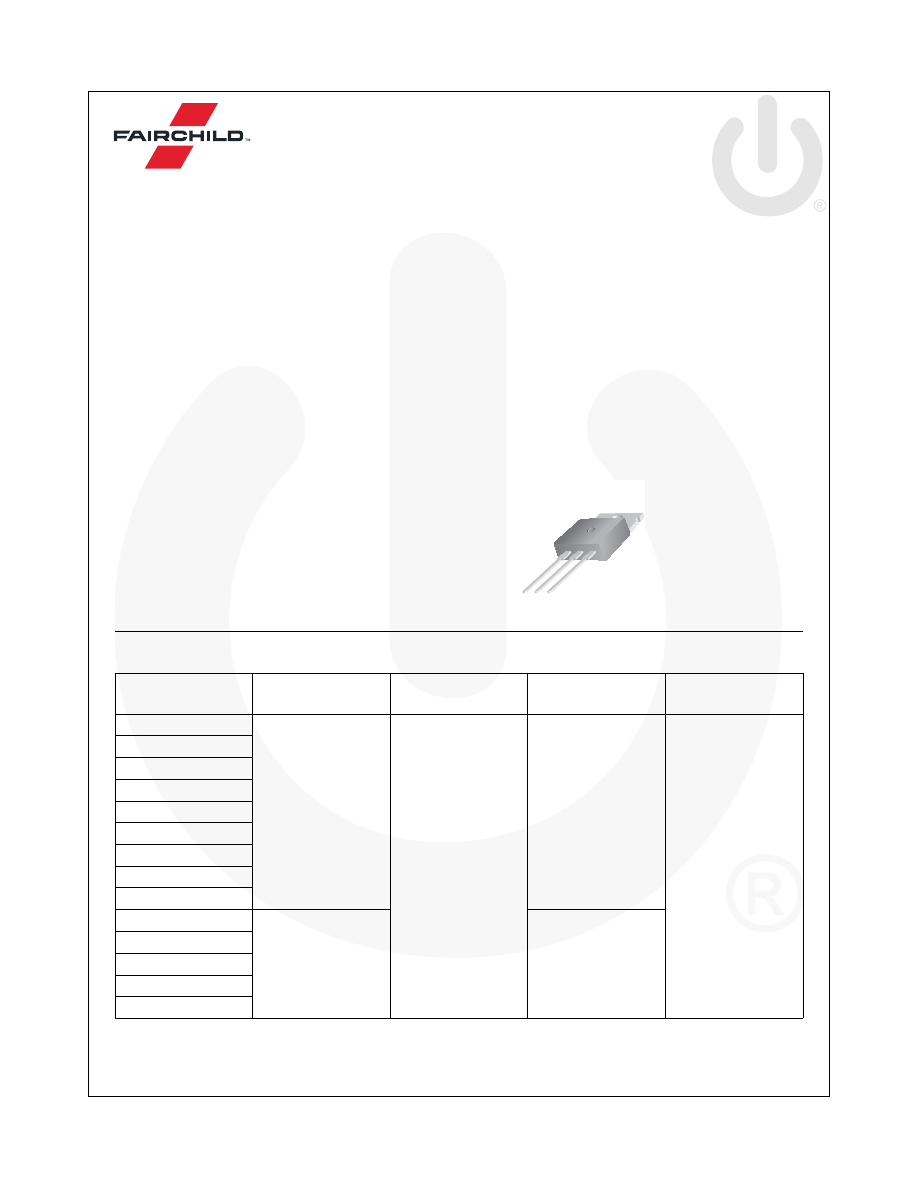
LM78XX / LM78XXA
3-T
e
rminal
1 A Positive V
o
lt
age Regulator
© 2006 Fairchild Semiconductor Corporation
www.fairchildsemi.com
LM78XX / LM78XXA Rev. 1.3.1
September 2014
LM78XX / LM78XXA
3-Terminal 1 A Positive Voltage Regulator
Features
Output Current up to 1 A
Output Voltages: 5, 6, 8, 9, 10, 12, 15, 18, 24 V
Thermal Overload Protection
Short-Circuit Protection
Output Transistor Safe Operating Area Protection
Ordering Information
(1)
Note:
1. Above output voltage tolerance is available at 25 °C.
Product Number
Output Voltage
Tolerance
Package
Operating
Temperature
Packing Method
LM7805CT
±4%
TO-220
(Single Gauge)
-40
°C to +125 °C
Rail
LM7806CT
LM7808CT
LM7809CT
LM7810CT
LM7812CT
LM7815CT
LM7818CT
LM7824CT
LM7805ACT
±2%
0
°C to +125 °C
LM7809ACT
LM7810ACT
LM7812ACT
LM7815ACT
Description
The LM78XX series of three-terminal positive regulators
is available in the TO-220 package and with several fixed
output voltages, making them useful in a wide range of
applications. Each type employs internal current limiting,
thermal shut-down, and safe operating area protection. If
adequate heat sinking is provided, they can deliver over
1 A output current. Although designed primarily as fixed-
voltage regulators, these devices can be used with exter-
nal components for adjustable voltages and currents.
1
1. Input
2. GND
3. Output
GND
TO-220
(Single Gauge)
LM78XX / LM78XXA
3-T
e
rminal
1 A Positive V
o
lt
age Regulator
© 2006 Fairchild Semiconductor Corporation
www.fairchildsemi.com
LM78XX / LM78XXA Rev. 1.3.1
2
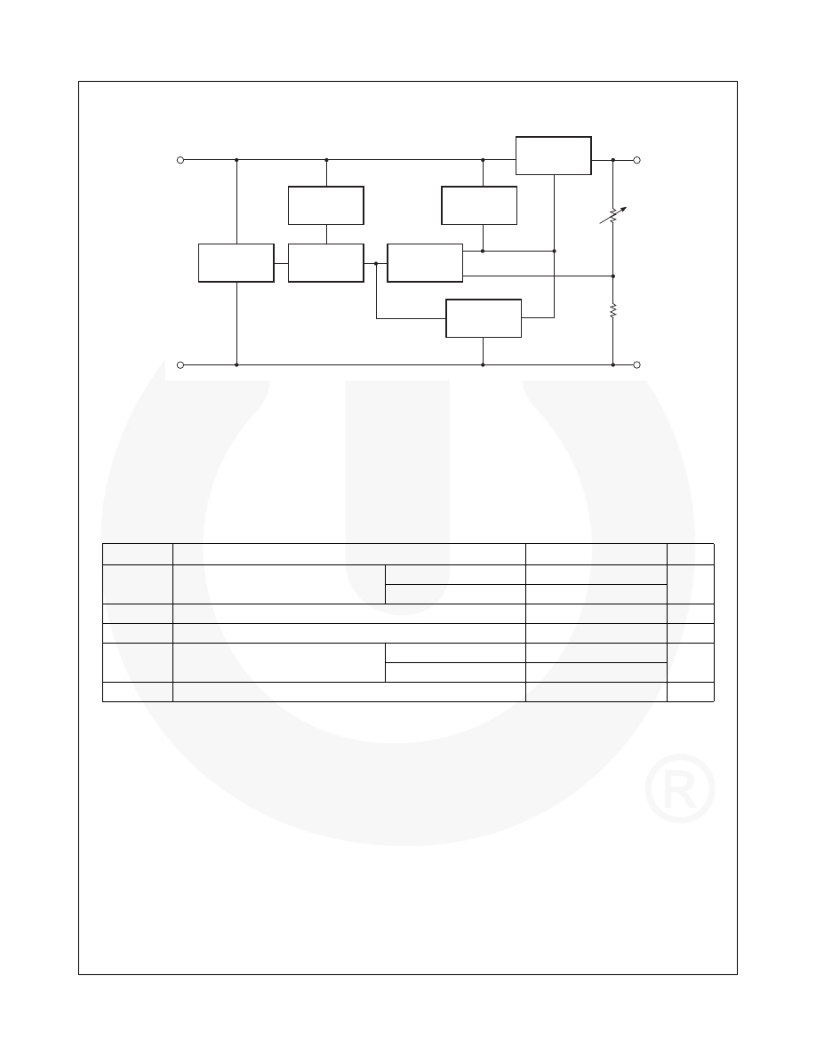
Block Diagram
Figure 1. Block Diagram
Absolute Maximum Ratings
Stresses exceeding the absolute maximum ratings may damage the device. The device may not function or be opera-
ble above the recommended operating conditions and stressing the parts to these levels is not recommended. In addi-
tion, extended exposure to stresses above the recommended operating conditions may affect device reliability. The
absolute maximum ratings are stress ratings only.
Values are at T
A
= 25 °C unless otherwise noted.
Symbol
Parameter
Value
Unit
V
I
Input Voltage
V
O
= 5 V to 18 V
35
V
V
O
= 24 V
40
R
ΘJC
Thermal Resistance, Junction-Case (TO-220)
5
°C/W
R
ΘJA
Thermal Resistance, Junction-Air
(TO-220)
65
°C/W
T
OPR
Operating Temperature Range
LM78xx
-40 to +125
°C
LM78xxA
0 to +125
T
STG
Storage Temperature Range
- 65 to +150
°C
Starting
Circuit
Input
1
Reference
Voltage
Current
Generator
SOA
Protection
Thermal
Protection
Series Pass
Element
Error
Amplifier
Output
3
GND
2
LM78XX / LM78XXA
3-T
e
rminal
1 A Positive V
o
lt
age Regulator
© 2006 Fairchild Semiconductor Corporation
www.fairchildsemi.com
LM78XX / LM78XXA Rev. 1.3.1
3
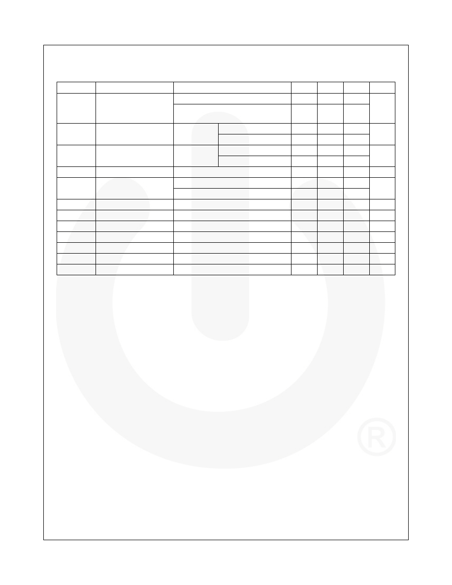
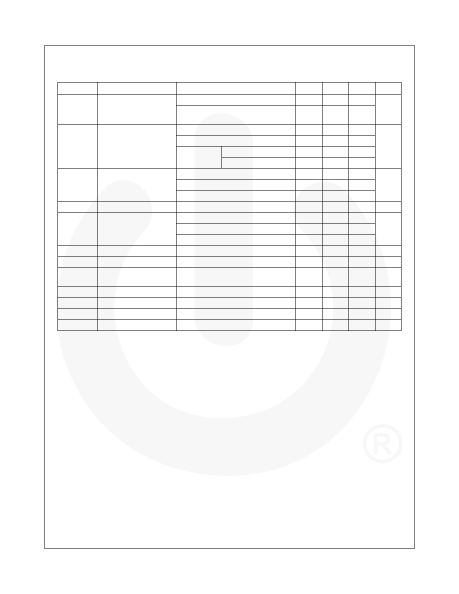
Electrical Characteristics (LM7805)
Refer to the test circuit, -40 °C < T
J
< 125 °C, I
O
= 500 mA, V
I
= 10 V, C
I
= 0.1
μF, unless otherwise specified.
Notes:
2. Load and line regulation are specified at constant junction temperature. Changes in V
O
due to heating effects
must be taken into account separately. Pulse testing with low duty is used.
3. These parameters, although guaranteed, are not 100% tested in production.
Symbol
Parameter
Conditions
Min.
Typ.
Max.
Unit
V
O
Output Voltage
T
J
= +25
°C
4.80
5.00
5.20
V
I
O
= 5 mA to 1 A, P
O
≤ 15 W,
V
I
= 7 V to 20 V
4.75
5.00
5.25
Regline
Line Regulation
(2)
T
J
= +25
°C
V
I
= 7 V to 25 V
4.0
100.0
mV
V
I
= 8 V to 12 V
1.6
50.0
Regload
Load Regulation
(2)
T
J
= +25
°C
I
O
= 5 mA to 1.5 A
9.0
100.0
mV
I
O
= 250 mA to 750 mA
4.0
50.0
I
Q
Quiescent Current
T
J
= +25
°C
5
8
mA
ΔI
Q
Quiescent Current
Change
I
O
= 5 mA to 1 A
0.03
0.50
mA
V
I
= 7 V to 25 V
0.30
1.30
ΔV
O
/
ΔT
Output Voltage Drift
(3)
I
O
= 5 mA
-0.8
mV/
°C
V
N
Output Noise Voltage
f = 10 Hz to 100 kHz, T
A
= +25
°C
42
μV
RR
Ripple Rejection
(3)
f = 120 Hz, V
I
= 8 V to 18 V
62
73
dB
V
DROP
Dropout Voltage
T
J
= +25
°C, I
O
= 1 A
2
V
R
O
Output Resistance
(3)
f = 1 kHz
15
m
Ω
I
SC
Short-Circuit Current
T
J
= +25
°C, V
I
= 35 V
230
mA
I
PK
Peak Current
(3)
T
J
= +25
°C
2.2
A

LM78XX / LM78XXA
3-T
e
rminal
1 A Positive V
o
lt
age Regulator
© 2006 Fairchild Semiconductor Corporation
www.fairchildsemi.com
LM78XX / LM78XXA Rev. 1.3.1
4
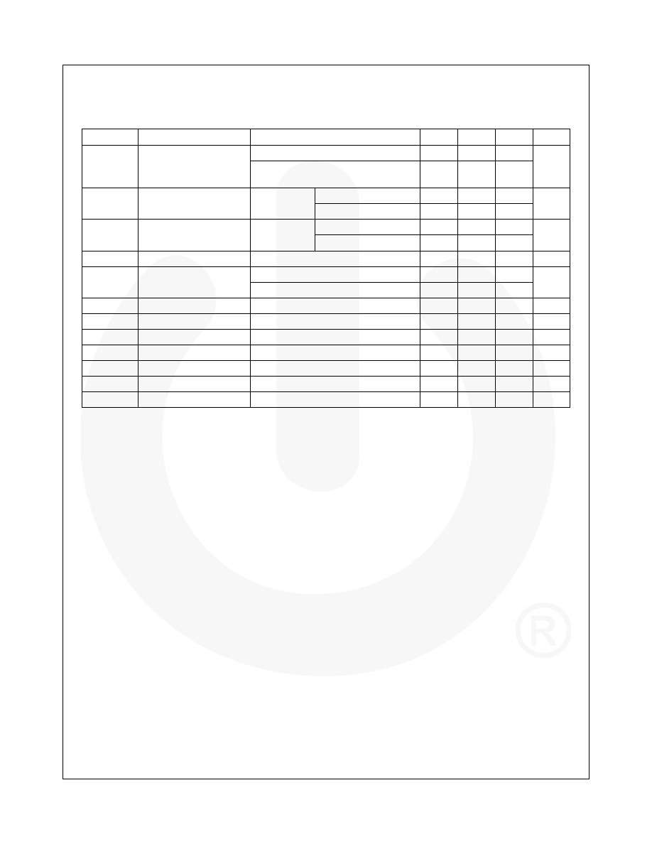
Electrical Characteristics (LM7806)
Refer to the test circuit, -40 °C < T
J
< 125 °C, I
O
= 500 mA, V
I
= 11 V, C
I
= 0.33
μF, C
O
= 0.1
μF, unless otherwise spec-
ified.
Notes:
4. Load and line regulation are specified at constant junction temperature. Changes in V
O
due to heating effects must
be taken into account separately. Pulse testing with low duty is used.
5. These parameters, although guaranteed, are not 100% tested in production.
Symbol
Parameter
Conditions
Min.
Typ.
Max.
Unit
V
O
Output Voltage
T
J
= +25
°C
5.75
6.00
6.25
V
I
O
= 5 mA to 1 A, P
O
≤ 15 W,
V
I
= 8.0 V to 21 V
5.70
6.00
6.30
Regline
Line Regulation
(4)
T
J
= +25
°C
V
I
= 8 V to 25 V
5.0
120.0
mV
V
I
= 9 V to 13 V
1.5
60.0
Regload
Load Regulation
(4)
T
J
= +25
°C
I
O
= 5 mA to 1.5 A
9.0
120.0
mV
I
O
= 250 mA to 750 mA
3.0
60.0
I
Q
Quiescent Current
T
J
= +25
°C
5
8
mA
ΔI
Q
Quiescent Current
Change
I
O
= 5 mA to 1 A
0.5
mA
V
I
= 8 V to 25 V
1.3
ΔV
O
/
ΔT
Output Voltage Drift
(5)
I
O
= 5 mA
-0.8
mV/
°C
V
N
Output Noise Voltage
f = 10 Hz to 100 kHz, T
A
= +25
°C
45
μV
RR
Ripple Rejection
(5)
f = 120 Hz, V
I
= 8 V to 18 V
62
73
dB
V
DROP
Dropout Voltage
T
J
= +25
°C, I
O
= 1 A
2
V
R
O
Output Resistance
(5)
f = 1 kHz
19
m
Ω
I
SC
Short-Circuit Current
T
J
= +25
°C, V
I
= 35 V
250
mA
I
PK
Peak Current
(5)
T
J
= +25
°C
2.2
A

LM78XX / LM78XXA
3-T
e
rminal
1 A Positive V
o
lt
age Regulator
© 2006 Fairchild Semiconductor Corporation
www.fairchildsemi.com
LM78XX / LM78XXA Rev. 1.3.1
5
Electrical Characteristics (LM7808)
Refer to the test circuit, -40 °C < T
J
< 125 °C, I
O
= 500 mA, V
I
= 14 V, C
I
= 0.33
μF, C
O
= 0.1
μF, unless otherwise spec-
ified.
Notes:
6. Load and line regulation are specified at constant junction temperature. Changes in V
O
due to heating effects must
be taken into account separately. Pulse testing with low duty is used.
7. These parameters, although guaranteed, are not 100% tested in production.
Symbol
Parameter
Conditions
Min.
Typ.
Max.
Unit
V
O
Output Voltage
T
J
= +25
°C
7.7
8.0
8.3
V
I
O
= 5 mA to 1 A, P
O
≤ 15 W,
V
I
= 10.5 V to 23 V
7.6
8.0
8.4
Regline
Line Regulation
(6)
T
J
= +25
°C
V
I
= 10.5 V to 25 V
5
160
mV
V
I
= 11.5 V to 17 V
2
80
Regload
Load Regulation
(6)
T
J
= +25
°C
I
O
= 5 mA to 1.5 A
10
160
mV
I
O
= 250 mA to 750 mA
5
80
I
Q
Quiescent Current
T
J
= +25
°C
5
8
mA
ΔI
Q
Quiescent Current
Change
I
O
= 5 mA to 1 A
0.05
0.50
mA
V
I
= 10.5 V to 25 V
0.5
1.0
ΔV
O
/
ΔT
Output Voltage Drift
(7)
I
O
= 5 mA
-0.8
mV/
°C
V
N
Output Noise Voltage
f = 10 Hz to 100 kHz, T
A
= +25
°C
52
μV
RR
Ripple Rejection
(7)
f = 120 Hz, V
I
= 11.5 V to 21.5 V
56
73
dB
V
DROP
Dropout Voltage
I
O
= 1 A, T
J
= +25
°C
2
V
R
O
Output Resistance
(7)
f = 1 kHz
17
m
Ω
I
SC
Short-Circuit Current
V
I
= 35 V, T
J
= +25
°C
230
mA
I
PK
Peak Current
(7)
T
J
= +25
°C
2.2
A

LM78XX / LM78XXA
3-T
e
rminal
1 A Positive V
o
lt
age Regulator
© 2006 Fairchild Semiconductor Corporation
www.fairchildsemi.com
LM78XX / LM78XXA Rev. 1.3.1
6
Electrical Characteristics (LM7809)
Refer to the test circuit, -40 °C < T
J
< 125 °C, I
O
= 500 mA, V
I
= 15 V, C
I
= 0.33
μF, C
O
= 0.1
μF, unless otherwise spec-
ified.
Notes:
8. Load and line regulation are specified at constant junction temperature. Changes in V
O
due to heating effects must
be taken into account separately. Pulse testing with low duty is used.
9. These parameters, although guaranteed, are not 100% tested in production.
Symbol
Parameter
Conditions
Min.
Typ.
Max.
Unit
V
O
Output Voltage
T
J
= +25
°C
8.65
9.00
9.35
V
I
O
= 5 mA to 1 A, P
O
≤ 15 W,
V
I
= 11.5 V to 24 V
8.60
9.00
9.40
Regline
Line Regulation
(8)
T
J
= +25
°C
V
I
= 11.5 V to 25 V
6
180
mV
V
I
= 12 V to 17 V
2
90
Regload
Load Regulation
(8)
T
J
= +25
°C
I
O
= 5 mA to 1.5 A
12
180
mV
I
O
= 250 mA to 750 mA
4
90
I
Q
Quiescent Current
T
J
= +25
°C
5
8
mA
ΔI
Q
Quiescent Current
Change
I
O
= 5 mA to 1 A
0.5
mA
V
I
= 11.5 V to 26 V
1.3
ΔV
O
/
ΔT
Output Voltage Drift
(9)
I
O
= 5 mA
-1
mV/
°C
V
N
Output Noise Voltage
f = 10 Hz to 100 kHz, T
A
= +25
°C
58
μV
RR
Ripple Rejection
(9)
f = 120 Hz, V
I
= 13 V to 23 V
56
71
dB
V
DROP
Dropout Voltage
I
O
= 1 A, T
J
= +25
°C
2
V
R
O
Output Resistance
(9)
f = 1 kHz
17
m
Ω
I
SC
Short-Circuit Current
V
I
= 35 V, T
J
= +25
°C
250
mA
I
PK
Peak Current
(9)
T
J
= +25
°C
2.2
A

LM78XX / LM78XXA
3-T
e
rminal
1 A Positive V
o
lt
age Regulator
© 2006 Fairchild Semiconductor Corporation
www.fairchildsemi.com
LM78XX / LM78XXA Rev. 1.3.1
7
Electrical Characteristics (LM7810)
Refer to the test circuit, -40 °C < T
J
< 125 °C, I
O
= 500 mA, V
I
= 16 V, C
I
= 0.33
μF, C
O
= 0.1
μF, unless otherwise spec-
ified.
Notes:
10. Load and line regulation are specified at constant junction temperature. Changes in V
O
due to heating effects must
be taken into account separately. Pulse testing with low duty is used.
11. These parameters, although guaranteed, are not 100% tested in production.
Symbol
Parameter
Conditions
Min.
Typ.
Max.
Unit
V
O
Output Voltage
T
J
= +25
°C
9.6
10.0
10.4
V
I
O
= 5 mA to 1 A, P
O
≤ 15 W,
V
I
= 12.5 V to 25 V
9.5
10.0
10.5
Regline
Line Regulation
(10)
T
J
= +25
°C
V
I
= 12.5 V to 25 V
10
200
mV
V
I
= 13 V to 25 V
3
100
Regload
Load Regulation
(10)
T
J
= +25
°C
I
O
= 5 mA to 1.5 A
12
200
mV
I
O
= 250 mA to 750 mA
4
400
I
Q
Quiescent Current
T
J
= +25
°C
5.1
8.0
mA
ΔI
Q
Quiescent Current
Change
I
O
= 5 mA to 1 A
0.5
mA
V
I
= 12.5 V to 29 V
1.0
ΔV
O
/
ΔT
Output Voltage Drift
(11)
I
O
= 5 mA
-1
mV/
°C
V
N
Output Noise Voltage
f = 10 Hz to 100 kHz, T
A
= +25
°C
58
μV
RR
Ripple Rejection
(11)
f = 120 Hz, V
I
= 13 V to 23 V
56
71
dB
V
DROP
Dropout Voltage
I
O
= 1 A, T
J
= +25
°C
2
V
R
O
Output Resistance
(11)
f = 1 kHz
17
m
Ω
I
SC
Short-Circuit Current
V
I
= 35 V, T
J
= +25
°C
250
mA
I
PK
Peak Current
(11)
T
J
= +25
°C
2.2
A
LM78XX / LM78XXA
3-T
e
rminal
1 A Positive V
o
lt
age Regulator
© 2006 Fairchild Semiconductor Corporation
www.fairchildsemi.com
LM78XX / LM78XXA Rev. 1.3.1
8
Electrical Characteristics (LM7812)
Refer to the test circuit, -40 °C < T
J
< 125 °C, I
O
= 500 mA, V
I
= 19 V, C
I
= 0.33
μF, C
O
= 0.1
μF, unless otherwise spec-
ified.
Notes:
12. Load and line regulation are specified at constant junction temperature. Changes in V
O
due to heating effects must
be taken into account separately. Pulse testing with low duty is used.
13. These parameters, although guaranteed, are not 100% tested in production.
Symbol
Parameter
Conditions
Min.
Typ.
Max.
Unit
V
O
Output Voltage
T
J
= +25
°C
11.5
12.0
12.5
V
I
O
= 5 mA to 1 A, P
O
≤ 15 W,
V
I
= 14.5 V to 27 V
11.4
12.0
12.6
Regline
Line Regulation
(12)
T
J
= +25
°C
V
I
= 14.5 V to 30 V
10
240
mV
V
I
= 16 V to 22 V
3
120
Regload
Load Regulation
(12)
T
J
= +25
°C
I
O
= 5 mA to 1.5 A
11
240
mV
I
O
= 250 mA to 750 mA
5
120
I
Q
Quiescent Current
T
J
= +25
°C
5.1
8.0
mA
ΔI
Q
Quiescent Current
Change
I
O
= 5 mA to 1 A
0.1
0.5
mA
V
I
= 14.5 V to 30 V
0.5
1.0
ΔV
O
/
ΔT
Output Voltage Drift
(13)
I
O
= 5 mA
-1
mV/
°C
V
N
Output Noise Voltage
f = 10 Hz to 100 kHz, T
A
= +25
°C
76
μV
RR
Ripple Rejection
(13)
f = 120 Hz, V
I
= 15 V to 25 V
55
71
dB
V
DROP
Dropout Voltage
I
O
= 1 A, T
J
= +25
°C
2
V
R
O
Output Resistance
(13)
f = 1 kHz
18
m
Ω
I
SC
Short-Circuit Current
V
I
= 35 V, T
J
= +25
°C
230
mA
I
PK
Peak Current
(13)
T
J
= +25
°C
2.2
A

LM78XX / LM78XXA
3-T
e
rminal
1 A Positive V
o
lt
age Regulator
© 2006 Fairchild Semiconductor Corporation
www.fairchildsemi.com
LM78XX / LM78XXA Rev. 1.3.1
9
Electrical Characteristics (LM7815)
Refer to the test circuit, -40 °C < T
J
< 125 °C, I
O
= 500 mA, V
I
= 23 V, C
I
= 0.33
μF, C
O
= 0.1
μF, unless otherwise spec-
ified.
Notes:
14. Load and line regulation are specified at constant junction temperature. Changes in V
O
due to heating effects must
be taken into account separately. Pulse testing with low duty is used.
15. These parameters, although guaranteed, are not 100% tested in production.
Symbol
Parameter
Conditions
Min.
Typ.
Max.
Unit
V
O
Output Voltage
T
J
= +25
°C
14.40
15.00
15.60
V
I
O
= 5 mA to 1 A, P
O
≤ 15 W,
V
I
= 17.5 V to 30 V
14.25
15.00
15.75
Regline
Line Regulation
(14)
T
J
= +25
°C
V
I
= 17.5 V to 30 V
11
300
mV
V
I
= 20 V to 26 V
3
150
Regload
Load Regulation
(14)
T
J
= +25
°C
I
O
= 5 mA to 1.5 A
12
300
mV
I
O
= 250 mA to 750 mA
4
150
I
Q
Quiescent Current
T
J
= +25
°C
5.2
8.0
mA
ΔI
Q
Quiescent Current
Change
I
O
= 5 mA to 1 A
0.5
mA
V
I
= 17.5 V to 30 V
1.0
ΔV
O
/
ΔT
Output Voltage Drift
(15)
I
O
= 5 mA
-1
mV/
°C
V
N
Output Noise Voltage
f = 10 Hz to 100 kHz, T
A
= +25
°C
90
μV
RR
Ripple Rejection
(15)
f = 120 Hz, V
I
= 18.5 V to 28.5 V
54
70
dB
V
DROP
Dropout Voltage
I
O
= 1 A, T
J
= +25
°C
2
V
R
O
Output Resistance
(15)
f = 1 kHz
19
m
Ω
I
SC
Short-Circuit Current
V
I
= 35 V, T
J
= +25
°C
250
mA
I
PK
Peak Current
(15)
T
J
= +25
°C
2.2
A

LM78XX / LM78XXA
3-T
e
rminal
1 A Positive V
o
lt
age Regulator
© 2006 Fairchild Semiconductor Corporation
www.fairchildsemi.com
LM78XX / LM78XXA Rev. 1.3.1
10
Electrical Characteristics (LM7818)
Refer to the test circuit, -40 °C < T
J
< 125 °C, I
O
= 500 mA, V
I
= 27 V, C
I
= 0.33
μF, C
O
= 0.1
μF, unless otherwise spec-
ified.
Notes:
16. Load and line regulation are specified at constant junction temperature. Changes in V
O
due to heating effects must
be taken into account separately. Pulse testing with low duty is used.
17. These parameters, although guaranteed, are not 100% tested in production.
Symbol
Parameter
Conditions
Min.
Typ.
Max.
Unit
V
O
Output Voltage
T
J
= +25
°C
17.3
18.0
18.7
V
I
O
= 5 mA to 1 A, P
O
≤ 15 W,
V
I
= 21 V to 33 V
17.1
18.0
18.9
Regline
Line Regulation
(16)
T
J
= +25
°C
V
I
= 21 V to 33 V
15
360
mV
V
I
= 24 V to 30 V
5
180
Regload
Load Regulation
(16)
T
J
= +25
°C
I
O
= 5 mA to 1.5 A
15
360
mV
I
O
= 250 mA to 750 mA
5
180
I
Q
Quiescent Current
T
J
= +25
°C
5.2
8.0
mA
ΔI
Q
Quiescent Current
Change
I
O
= 5 mA to 1 A
0.5
mA
V
I
= 21 V to 33 V
1.0
ΔV
O
/
ΔT
Output Voltage Drift
(17)
I
O
= 5 mA
-1
mV/
°C
V
N
Output Noise Voltage
f = 10 Hz to 100 kHz, T
A
= +25
°C
110
μV
RR
Ripple Rejection
(17)
f = 120 Hz, V
I
= 22 V to 32 V
53
69
dB
V
DROP
Dropout Voltage
I
O
= 1 A, T
J
= +25
°C
2
V
R
O
Output Resistance
(17)
f = 1 kHz
22
m
Ω
I
SC
Short-Circuit Current
V
I
= 35 V, T
J
= +25
°C
250
mA
I
PK
Peak Current
(17)
T
J
= +25
°C
2.2
A

LM78XX / LM78XXA
3-T
e
rminal
1 A Positive V
o
lt
age Regulator
© 2006 Fairchild Semiconductor Corporation
www.fairchildsemi.com
LM78XX / LM78XXA Rev. 1.3.1
11
Electrical Characteristics (LM7824)
Refer to the test circuit, -40 °C < T
J
< 125 °C, I
O
= 500 mA, V
I
= 33 V, C
I
= 0.33
μF, C
O
= 0.1
μF, unless otherwise spec-
ified.
Notes:
18. Load and line regulation are specified at constant junction temperature. Changes in V
O
due to heating effects must
be taken into account separately. Pulse testing with low duty is used.
19. These parameters, although guaranteed, are not 100% tested in production.
Symbol
Parameter
Conditions
Min.
Typ.
Max.
Unit
V
O
Output Voltage
T
J
= +25
°C
23.00
24.00
25.00
V
I
O
= 5 mA to 1 A, P
O
≤ 15 W,
V
I
= 27 V to 38 V
22.80
24.00
25.25
Regline
Line Regulation
(18)
T
J
= +25
°C
V
I
= 27 V to 38 V
17
480
mV
V
I
= 30 V to 36 V
6
240
Regload
Load Regulation
(18)
T
J
= +25
°C
I
O
= 5 mA to 1.5 A
15
480
mV
I
O
= 250 mA to 750 mA
5
240
I
Q
Quiescent Current
T
J
= +25
°C
5.2
8.0
mA
ΔI
Q
Quiescent Current
Change
I
O
= 5 mA to 1 A
0.1
0.5
mA
V
I
= 27 V to 38 V
0.5
1.0
ΔV
O
/
ΔT
Output Voltage Drift
(19)
I
O
= 5 mA
-1.5
mV/
°C
V
N
Output Noise Voltage
f = 10 Hz to 100 kHz, T
A
= +25
°C
120
μV
RR
Ripple Rejection
(19)
f = 120 Hz, V
I
= 28 V to 38 V
50
67
dB
V
DROP
Dropout Voltage
I
O
= 1 A, T
J
= +25
°C
2
V
R
O
Output Resistance
(19)
f = 1 kHz
28
m
Ω
I
SC
Short-Circuit Current
V
I
= 35 V, T
J
= +25
°C
230
mA
I
PK
Peak Current
(19)
T
J
= +25
°C
2.2
A

LM78XX / LM78XXA
3-T
e
rminal
1 A Positive V
o
lt
age Regulator
© 2006 Fairchild Semiconductor Corporation
www.fairchildsemi.com
LM78XX / LM78XXA Rev. 1.3.1
12
Electrical Characteristics (LM7805A)
Refer to the test circuit, 0 °C < T
J
< 125 °C, I
O
= 1 A, V
I
= 10 V, C
I
= 0.33
μF, C
O
= 0.1
μF, unless otherwise specified.
Notes:
20. Load and line regulation are specified at constant junction temperature. Changes in V
O
due to heating effects must
be taken into account separately. Pulse testing with low duty is used.
21. These parameters, although guaranteed, are not 100% tested in production.
Symbol
Parameter
Conditions
Min.
Typ.
Max.
Unit
V
O
Output Voltage
T
J
= +25
°C
4.9
5.0
5.1
V
I
O
= 5 mA to 1 A, P
O
≤ 15 W,
V
I
= 7.5 V to 20 V
4.8
5.0
5.2
Regline
Line Regulation
(20)
V
I
= 7.5 V to 25 V, I
O
= 500 mA
5.0
50.0
mV
V
I
= 8 V to 12 V
3.0
50.0
T
J
= +25
°C
V
I
= 7.3 V to 20 V
5.0
50.0
V
I
= 8 V to 12 V
1.5
25.0
Regload
Load Regulation
(20)
T
J
= +25
°C, I
O
= 5 mA to 1.5 A
9
100
mV
I
O
= 5 mA to 1 A
9
100
I
O
= 250 mA to 750 mA
4
50
I
Q
Quiescent Current
T
J
= +25
°C
5
6
mA
ΔI
Q
Quiescent Current
Change
I
O
= 5 mA to 1 A
0.5
mA
V
I
= 8 V to 25 V, I
O
= 500 mA
0.8
V
I
= 7.5 V to 20 V, T
J
= +25
°C
0.8
ΔV
O
/
ΔT
Output Voltage Drift
(21)
I
O
= 5 mA
-0.8
mV/
°C
V
N
Output Noise Voltage
f = 10 Hz to 100 kHz, T
A
= +25
°C
42
μV
RR
Ripple Rejection
(21)
f = 120 Hz, V
O
= 500 mA,
V
I
=8 V to 18 V
68
dB
V
DROP
Dropout Voltage
I
O
= 1 A, T
J
= +25
°C
2
V
R
O
Output Resistance
(21)
f = 1 kHz
17
m
Ω
I
SC
Short-Circuit Current
V
I
= 35 V, T
J
= +25
°C
250
mA
I
PK
Peak Current
(21)
T
J
= +25
°C
2.2
A

LM78XX / LM78XXA
3-T
e
rminal
1 A Positive V
o
lt
age Regulator
© 2006 Fairchild Semiconductor Corporation
www.fairchildsemi.com
LM78XX / LM78XXA Rev. 1.3.1
13
Electrical Characteristics (LM7809A)
Refer to the test circuit, 0 °C < T
J
< 125 °C, I
O
= 1 A, V
I
= 15 V, C
I
= 0.33
μF, C
O
= 0.1
μF, unless otherwise specified.
Notes:
22. Load and line regulation are specified at constant junction temperature. Changes in V
O
due to heating effects must
be taken into account separately. Pulse testing with low duty is used.
23. These parameters, although guaranteed, are not 100% tested in production.
Symbol
Parameter
Conditions
Min.
Typ.
Max.
Unit
V
O
Output Voltage
T
J
= +25
°C
8.82
9.00
9.16
V
I
O
= 5 mA to 1 A, P
O
≤ 15 W,
V
I
= 11.2 V to 24 V
8.65
9.00
9.35
Regline
Line Regulation
(22)
V
I
= 11.7 V to 25 V, I
O
= 500 mA
6
90
mV
V
I
= 12.5 V to 19 V
4
45
T
J
= +25
°C
V
I
= 11.5 V to 24 V
6
90
V
I
= 12.5 V to 19 V
2
45
Regload
Load Regulation
(22)
T
J
= +25
°C, I
O
= 5 mA to 1.5 A
12
100
mV
I
O
= 5 mA to 1 A
12
100
I
O
= 250 mA to 750 mA
5
50
I
Q
Quiescent Current
T
J
= +25
°C
5
6
mA
ΔI
Q
Quiescent Current
Change
I
O
= 5 mA to 1 A
0.5
mA
V
I
= 12 V to 25 V, I
O
= 500 mA
0.8
V
I
= 11.7 V to 25 V, T
J
= +25
°C
0.8
ΔV
O
/
ΔT
Output Voltage Drift
(23)
I
O
= 5 mA
-1
mV/
°C
V
N
Output Noise Voltage
f = 10 Hz to 100 kHz, T
A
= +25
°C
58
μV
RR
Ripple Rejection
(23)
f = 120 Hz, V
O
= 500 mA,
V
I
=12 V to 22 V
62
dB
V
DROP
Dropout Voltage
I
O
= 1 A, T
J
= +25
°C
2
V
R
O
Output Resistance
(23)
f = 1 kHz
17
m
Ω
I
SC
Short-Circuit Current
V
I
= 35 V, T
J
= +25
°C
250
mA
I
PK
Peak Current
(23)
T
J
= +25
°C
2.2
A

LM78XX / LM78XXA
3-T
e
rminal
1 A Positive V
o
lt
age Regulator
© 2006 Fairchild Semiconductor Corporation
www.fairchildsemi.com
LM78XX / LM78XXA Rev. 1.3.1
14
Electrical Characteristics (LM7810A)
Refer to the test circuit, 0 °C < T
J
< 125 °C, I
O
= 1 A, V
I
= 16 V, C
I
= 0.33
μF, C
O
= 0.1
μF, unless otherwise specified.
Notes:
24. Load and line regulation are specified at constant junction temperature. Changes in V
O
due to heating effects must
be taken into account separately. Pulse testing with low duty is used.
25. These parameters, although guaranteed, are not 100% tested in production.
Symbol
Parameter
Conditions
Min.
Typ.
Max.
Unit
V
O
Output Voltage
T
J
= +25
°C
9.8
10.0
10.2
V
I
O
= 5 mA to 1 A, P
O
≤ 15 W,
V
I
= 12.8 V to 25 V
9.6
10.0
10.4
Regline
Line Regulation
(24)
V
I
= 12.8 V to 26 V, I
O
= 500 mA
8
100
mV
V
I
= 13 V to 20 V
4
50
T
J
= +25
°C
V
I
= 12.5 V to 25 V
8
100
V
I
= 13 V to 20 V
3
50
Regload
Load Regulation
(24)
T
J
= +25
°C, I
O
= 5 mA to 1.5 A
12
100
mV
I
O
= 5 mA to 1 A
12
100
I
O
= 250 mA to 750 mA
5
50
I
Q
Quiescent Current
T
J
= +25
°C
5
6
mA
ΔI
Q
Quiescent Current
Change
I
O
= 5 mA to 1 A
0.5
mA
V
I
= 12.8 V to 25 V, I
O
= 500 mA
0.8
V
I
= 13 V to 26 V, T
J
= +25
°C
0.5
ΔV
O
/
ΔT
Output Voltage Drift
(25)
I
O
= 5 mA
-1
mV/
°C
V
N
Output Noise Voltage
f = 10 Hz to 100 kHz, T
A
= +25
°C
58
μV
RR
Ripple Rejection
(25)
f = 120 Hz, V
O
= 500 mA,
V
I
=14 V to 24 V
62
dB
V
DROP
Dropout Voltage
I
O
= 1 A, T
J
= +25
°C
2
V
R
O
Output Resistance
(25)
f = 1 kHz
17
m
Ω
I
SC
Short-Circuit Current
V
I
= 35 V, T
J
= +25
°C
250
mA
I
PK
Peak Current
(25)
T
J
= +25
°C
2.2
A
LM78XX / LM78XXA
3-T
e
rminal
1 A Positive V
o
lt
age Regulator
© 2006 Fairchild Semiconductor Corporation
www.fairchildsemi.com
LM78XX / LM78XXA Rev. 1.3.1
15
Electrical Characteristics (LM7812A)
Refer to the test circuit, 0 °C < T
J
< 125 °C, I
O
= 1 A, V
I
= 19 V, C
I
= 0.33
μF, C
O
= 0.1
μF, unless otherwise specified.
Notes:
26. Load and line regulation are specified at constant junction temperature. Changes in V
O
due to heating effects must
be taken into account separately. Pulse testing with low duty is used.
27. These parameters, although guaranteed, are not 100% tested in production.
Symbol
Parameter
Conditions
Min.
Typ.
Max.
Unit
V
O
Output Voltage
T
J
= +25
°C
11.75
12.00
12.25
V
I
O
= 5 mA to 1 A, P
O
≤ 15 W,
V
I
= 14.8 V to 27 V
11.50
12.00
12.50
Regline
Line Regulation
(26)
V
I
= 14.8 V to 30 V, I
O
= 500 mA
10
120
mV
V
I
= 16 V to 22 V
4
120
T
J
= +25
°C
V
I
= 14.5 V to 27 V
10
120
V
I
= 16 V to 22 V
3
60
Regload
Load Regulation
(26)
T
J
= +25
°C, I
O
= 5 mA to 1.5 A
12
100
mV
I
O
= 5 mA to 1 A
12
100
I
O
= 250 mA to 750 mA
5
50
I
Q
Quiescent Current
T
J
= +25
°C
5
6
mA
ΔI
Q
Quiescent Current
Change
I
O
= 5 mA to 1 A
0.5
mA
V
I
= 14 V to 27 V, I
O
= 500 mA
0.8
V
I
= 15 V to 30 V, T
J
= +25
°C
0.8
ΔV
O
/
ΔT
Output Voltage Drift
(27)
I
O
= 5 mA
-1
mV/
°C
V
N
Output Noise Voltage
f = 10 Hz to 100 kHz, T
A
= +25
°C
76
μV
RR
Ripple Rejection
(27)
f = 120 Hz, V
O
= 500 mA,
V
I
=14 V to 24 V
60
dB
V
DROP
Dropout Voltage
I
O
= 1 A, T
J
= +25
°C
2
V
R
O
Output Resistance
(27)
f = 1 kHz
18
m
Ω
I
SC
Short-Circuit Current
V
I
= 35 V, T
J
= +25
°C
250
mA
I
PK
Peak Current
(27)
T
J
= +25
°C
2.2
A

LM78XX / LM78XXA
3-T
e
rminal
1 A Positive V
o
lt
age Regulator
© 2006 Fairchild Semiconductor Corporation
www.fairchildsemi.com
LM78XX / LM78XXA Rev. 1.3.1
16
Electrical Characteristics (LM7815A)
Refer to the test circuit, 0 °C < T
J
< 125 °C, I
O
= 1 A, V
I
= 23 V, C
I
= 0.33
μF, C
O
= 0.1
μF, unless otherwise specified.
Notes:
28. Load and line regulation are specified at constant junction temperature. Changes in V
O
due to heating effects must
be taken into account separately. Pulse testing with low duty is used.
29. These parameters, although guaranteed, are not 100% tested in production.
Symbol
Parameter
Conditions
Min.
Typ.
Max.
Unit
V
O
Output Voltage
T
J
= +25
°C
14.75
15.00
15.30
V
I
O
= 5 mA to 1 A, P
O
≤ 15 W,
V
I
= 17.7 V to 30 V
14.40
15.00
15.60
Regline
Line Regulation
(28)
V
I
= 17.4 V to 30 V, I
O
= 500 mA
10
150
mV
V
I
= 20 V to 26 V
5
150
T
J
= +25
°C
V
I
= 17.5 V to 30 V
11
150
V
I
= 20 V to 26 V
3
75
Regload
Load Regulation
(28)
T
J
= +25
°C, I
O
= 5 mA to 1.5 A
12
100
mV
I
O
= 5 mA to 1 A
12
100
I
O
= 250 mA to 750 mA
5
50
I
Q
Quiescent Current
T
J
= +25
°C
5.2
6.0
mA
ΔI
Q
Quiescent Current
Change
I
O
= 5 mA to 1 A
0.5
mA
V
I
= 17.5 V to 30 V, I
O
= 500 mA
0.8
V
I
= 17.5 V to 30 V, T
J
= +25
°C
0.8
ΔV
O
/
ΔT
Output Voltage Drift
(29)
I
O
= 5 mA
-1
mV/
°C
V
N
Output Noise Voltage
f = 10 Hz to 100 kHz, T
A
= +25
°C
90
μV
RR
Ripple Rejection
(29)
f = 120 Hz, V
O
= 500 mA,
V
I
=18.5 V to 28.5 V
58
dB
V
DROP
Dropout Voltage
I
O
= 1 A, T
J
= +25
°C
2
V
R
O
Output Resistance
(29)
f = 1 kHz
19
m
Ω
I
SC
Short-Circuit Current
V
I
= 35 V, T
J
= +25
°C
250
mA
I
PK
Peak Current
(29)
T
J
= +25
°C
2.2
A
LM78XX / LM78XXA
3-T
e
rminal
1 A Positive V
o
lt
age Regulator
© 2006 Fairchild Semiconductor Corporation
www.fairchildsemi.com
LM78XX / LM78XXA Rev. 1.3.1
17
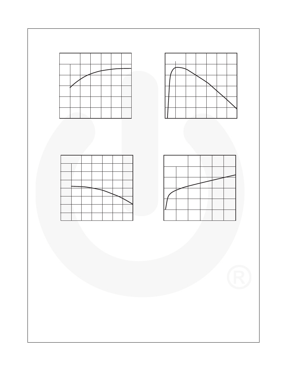
Typical Performance Characteristics
Figure 2. Quiescent Current
Figure 3. Peak Output Current
Figure 4. Output Voltage
Figure 5. Quiescent Current
6
5.75
5.5
5.25
5
4.75
4.5
V
I
= 10V
V
O
= 5V
I
O
= 5mA
-25
-50
0
25
50
75
100
125
QUIESCENT CURRENT (mA)
JUNCTION TEMPERATURE ( °C)
0
3
2.5
2
1.5
1
.5
0
T
J
= 25
°C
ΔV
O
= 100mV
5
10
15
20
25
30
35
OUTPUT CURRENT (A)
INPUT-OUTPUT DIFFERENTIAL (V)
1.02
1.01
1
0.99
0.98
V
I
- V
O
= 5V
I
O
= 5mA
-25
-50
0
25
50
75
100
125
NORMALIZED OUTPUT VOLTAGE (V)
JUNCTION TEMPERATURE ( °C)
7
6.5
6
5.5
5
4.5
4
T
J
= 25
°C
V
O
= 5V
I
O
= 10mA
10
5
15
20
25
30
35
QUIESCENT CURRENT (mA)
INPUT VOLTAGE (V)
LM78XX / LM78XXA
3-T
e
rminal
1 A Positive V
o
lt
age Regulator
© 2006 Fairchild Semiconductor Corporation
www.fairchildsemi.com
LM78XX / LM78XXA Rev. 1.3.1
18
Typical Applications
Figure 6. DC Parameters
Figure 7. Load Regulation
Figure 8. Ripple Rejection
0.1
μF
C
O
C
I
0.33
μF
Output
Input
LM78XX
1
3
2
LM78XX
3
2
1
0.33μF
270pF
100
Ω
30μS
R
L
2N6121
or EQ
Output
Input
V
O
0V
V
O
LM78XX
Output
Input
5.1
Ω
0.33μF
2
3
1
R
L
470μF
120Hz
+
LM78XX / LM78XXA
3-T
e
rminal
1 A Positive V
o
lt
age Regulator
© 2006 Fairchild Semiconductor Corporation
www.fairchildsemi.com
LM78XX / LM78XXA Rev. 1.3.1
19
Typical Applications
(Continued)
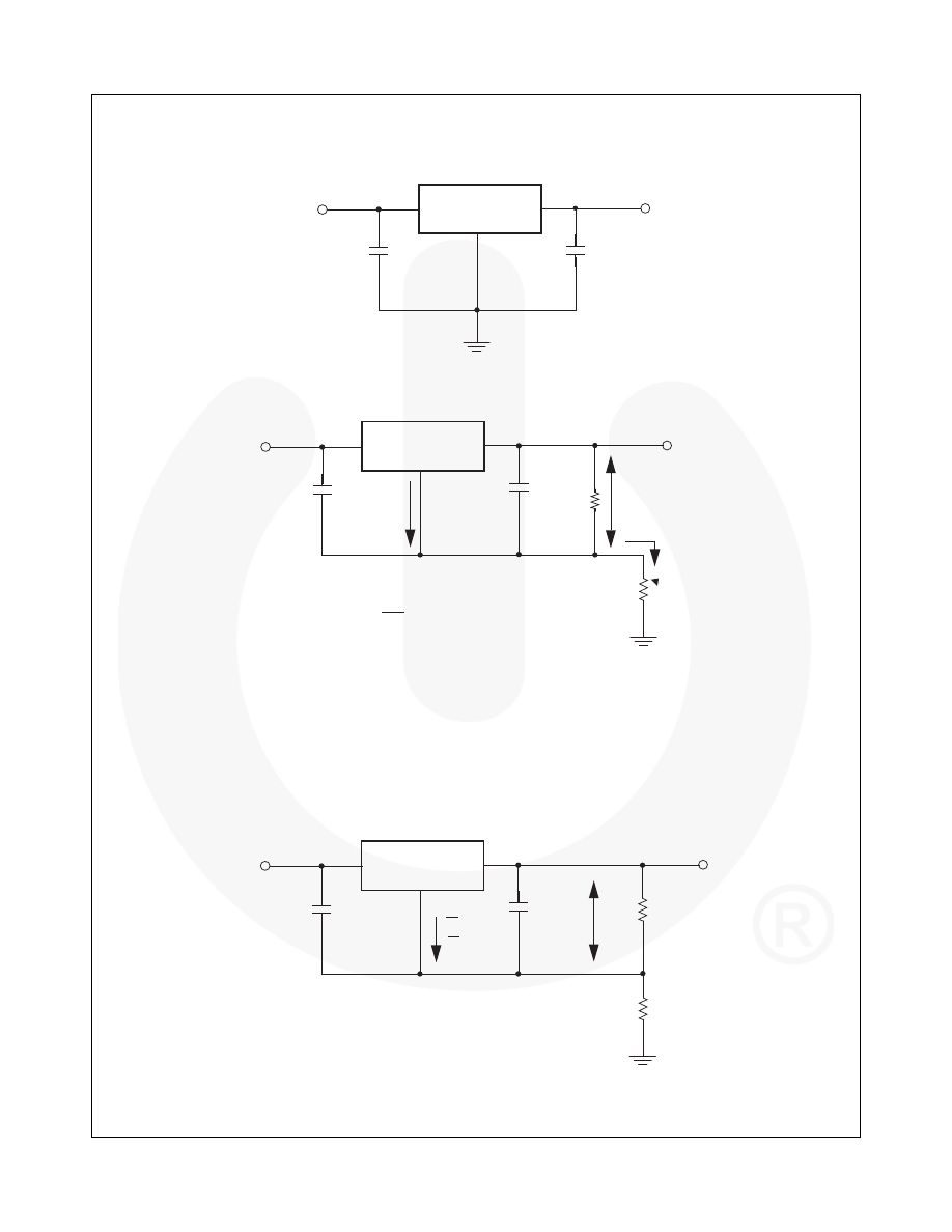
Figure 9. Fixed-Output Regulator
Figure 10. Constant Current Regulator
Notes:
29. To specify an output voltage, substitute voltage value for XX. A common ground is required between the input and
the output voltage. The input voltage must remain typically 2.0 V above the output voltage even during the low point
on the input ripple voltage.
30. C
I
is required if regulator is located an appreciable distance from power supply filter.
31. C
O
improves stability and transient response.
Figure 11. Circuit for Increasing Output Voltage
0.1
μF
C
O
C
I
0.33
μF
Output
Input
LM78XX
1
3
2
0.1
μF
C
O
C
I
0.33
μF
Output
Input
LM78XX
1
3
2
V
XX
R
1
R
L
I
Q
I
O
I
O
=
R
1
+ I
Q
V
XX
0.1
μF
C
O
C
I
0.33
μF
Output
Input
LM78XX
1
3
2
V
XX
R1
R2
I
Q
I
RI
≥ 5 I
Q
V
O
= V
XX
(1
+
R
2
/
R
1
)
+
I
Q
R
2
LM78XX / LM78XXA
3-T
e
rminal
1 A Positive V
o
lt
age Regulator
© 2006 Fairchild Semiconductor Corporation
www.fairchildsemi.com
LM78XX / LM78XXA Rev. 1.3.1
20
Typical Applications
(Continued)
Figure 12. Adjustable Output Regulator (7 V to 30 V)
Figure 13. High-Current Voltage Regulator
Figure 14. High Output Current with Short-Circuit Protection
LM741
-
+
2
3
6
4
2
3
1
0.33
μF
C
I
Input
Output
0.1
μF
C
O
LM7805
10kΩ
I
RI
≥ 5 I
Q
V
O
= V
XX
(1
+
R
2
/
R
1
)
+
I
Q
R
2
3
2
1
LM78XX
Output
Input
R1
3
Ω
0.33μF
IREG
0.1μF
I
O
IQ1
I
O
= I
REG
+ B
Q1
(I
REG
-V
BEQ1
/R
1
)
Q1 BD536
R1 =
V
BEQ1
I
REG
-I
Q1
B
Q1
/
LM78XX
Output
0.1μF
0.33μF
R1
3
Ω
3
2
1
Q1
Input
Q2
Q1 = TIP42
Q2 = TIP42
R
SC
=
I
SC
V
BEQ2
R
SC
LM78XX / LM78XXA
3-T
e
rminal
1 A Positive V
o
lt
age Regulator
© 2006 Fairchild Semiconductor Corporation
www.fairchildsemi.com
LM78XX / LM78XXA Rev. 1.3.1
21
Typical Applications
(Continued)
Figure 15. Tracking Voltage Regulator
Figure 16. Split Power Supply ( ±15 V - 1 A)
LM78XX
LM741
0.1μF
0.33μF
1
2
3
7
2
6
4
3
4.7k
Ω
4.7k
Ω
TIP42
COMMON
COMMON
V
O
-V
O
V
I
-V
IN
_
+
3
1
2
1
3
2
0.33μF
0.1μF
2.2μF
1μF +
+
1N4001
1N4001
+15V
-15V
+20V
-20V
LM7815
MC7915
LM78XX / LM78XXA
3-T
e
rminal
1 A Positive V
o
lt
age Regulator
© 2006 Fairchild Semiconductor Corporation
www.fairchildsemi.com
LM78XX / LM78XXA Rev. 1.3.1
22
Typical Applications
(Continued)
Figure 17. Negative Output Voltage Circuit
Figure 18. Switching Regulator
LM78XX
Output
Input
+
1
2
0.1μF
3
LM78XX
1mH
3
1
2
2000μF
Output
Input
D45H11
0.33μF
470
Ω
4.7
Ω
10μF
0.5
Ω
Z1
+
+
LM78XX / LM78XXA
3-T
e
rminal
1 A Positive V
o
lt
age Regulator
© 2006 Fairchild Semiconductor Corporation
www.fairchildsemi.com
LM78XX / LM78XXA Rev. 1.3.1
23
Physical Dimensions
Figure 19. TO-220, MOLDED, 3-LEAD, JEDEC VARIATION AB (ACTIVE)
© Fairchild Semiconductor Corporation
www.fairchildsemi.com
TRADEMARKS
The following includes registered and unregistered trademarks and service marks, owned by Fairchild Semiconductor and/or its global subsidiaries, and is not
intended to be an exhaustive list of all such trademarks.
AccuPower ¥
Awinda
®
AX-CAP
®
*
BitSiC ¥
Build it Now ¥
CorePLUS ¥
CorePOWER ¥
CROSSVOLT ¥
CTL ¥
Current Transfer Logic ¥
DEUXPEED
®
Dual Cool™
EcoSPARK
®
EfficientMax ¥
ESBC ¥
Fairchild
®
Fairchild Semiconductor
®
FACT Quiet Series ¥
FACT
®
FAST
®
FastvCore ¥
FETBench ¥
FPS ¥
F-PFS ¥
FRFET
®
Global Power Resource
SM
GreenBridge ¥
Green FPS ¥
Green FPS ¥ e-Series ¥
Gmax ¥
GTO ¥
IntelliMAX ¥
ISOPLANAR ¥
Making Small Speakers Sound Louder
and Better™
MegaBuck ¥
MICROCOUPLER ¥
MicroFET ¥
MicroPak ¥
MicroPak2 ¥
MillerDrive ¥
MotionMax ¥
MotionGrid
®
MTi
®
MTx
®
MVN
®
mWSaver
®
OptoHiT ¥
®
PowerTrench
®
PowerXS™
Programmable Active Droop ¥
QFET
®
QS ¥
Quiet Series ¥
RapidConfigure ¥
¥
Saving our world, 1mW/W/kW at a time™
SignalWise ¥
SmartMax ¥
SMART START ¥
Solutions for Your Success ¥
SPM
®
STEALTH ¥
SuperFET
®
SuperSOT ¥-3
SuperSOT ¥-6
SuperSOT ¥-8
SupreMOS
®
SyncFET ¥
Sync-Lock™
®*
TinyBoost
®
TinyBuck
®
TinyCalc ¥
TinyLogic
®
TINYOPTO ¥
TinyPower ¥
TinyPWM ¥
TinyWire ¥
TranSiC ¥
TriFault Detect ¥
TRUECURRENT
®
*
μSerDes ¥
UHC
®
Ultra FRFET ¥
UniFET ¥
VCX ¥
VisualMax ¥
VoltagePlus ¥
XS™
Xsens™
௺
™
* Trademarks of System General Corporation, used under license by Fairchild Semiconductor.
DISCLAIMER
FAIRCHILD SEMICONDUCTOR RESERVES THE RIGHT TO MAKE CHANGES WITHOUT FURTHER NOTICE TO ANY PRODUCTS HEREIN TO IMPROVE
RELIABILITY, FUNCTION, OR DESIGN. T
O OBTAIN THE LATEST, MOST UP-TO-DATE DATASHEET AND PRODUCT INFORMATION, VISIT OUR WEBSITE
AT
HTTP://WWW.FAIRCHILDSEMI.COM.
FAIRCHILD DOES NOT ASSUME ANY LIABILITY ARISING OUT OF THE APPLICATION OR USE OF ANY
PRODUCT OR CIRCUIT DESCRIBED HEREIN; NEITHER DOES IT CONVEY ANY LICENSE UNDER ITS PATENT RIGHTS, NOR THE RIGHTS OF OTHERS.
THESE SPECIFICATIONS DO NOT EXPAND THE TERMS OF FAIRCHILDS WORLDWIDE TERMS AND CONDITIONS, SPECIFICALLY THE WARRANTY
THEREIN, WHICH COVERS THESE PRODUCTS.
LIFE SUPPORT POLICY
FAIRCHILDS PRODUCTS ARE NOT AUTHORIZED FOR USE AS CRITICAL COMPONENTS IN LIFE SUPPORT DEVICES OR SYSTEMS WITHOUT THE
EXPRESS WRITTEN APPROVAL OF FAIRCHILD SEMICONDUCTOR CORPORATION.
As used herein:
1. Life support devices or systems are devices or systems which, (a) are
intended for surgical implant into the body or (b) support or sustain
life, and (c) whose failure to perform when properly used in
accordance with instructions for use provided in the labeling, can be
reasonably expected to result in a significant injury of the user.
2. A critical component in any component of a life support, device, or
system whose failure to perform can be reasonably expected to
cause the failure of the life support device or system, or to affect its
safety or effectiveness.
ANTI-COUNTERFEITING POLICY
Fairchild Semiconductor Corporation's Anti-Counterfeiting Policy. Fairchild's Anti-Counterfeiting Policy is also stated on our external website, www.fairchildsemi.com,
under Sales Support.
Counterfeiting of semiconductor parts is a growing problem in the industry. All manufacturers of semiconductor products are experiencing counterfeiting of their
parts. Customers who inadvertently purchase counterfeit parts experience many problems such as loss of brand reputation, substandard performance, failed
applications, and increased cost of production and manufacturing delays. Fairchild is taking strong measures to protect ourselves and our customers from the
proliferation of counterfeit parts. Fairchild strongly encourages customers to purchase Fairchild parts either directly from Fairchild or from Authorized Fairchild
Distributors who are listed by country on our web page cited above. Products customers buy either from Fairchild directly or from Authorized Fairchild Distributors
are genuine parts, have full traceability, meet Fairchild's quality standards for handling and storage and provide access to Fairchild's full range of up-to-date technical
and product information. Fairchild and our Authorized Distributors will stand behind all warranties and will appropriately address any warranty issues that may arise.
Fairchild will not provide any warranty coverage or other assistance for parts bought from Unauthorized Sources. Fairchild is committed to combat this global
problem and encourage our customers to do their part in stopping this practice by buying direct or from authorized distributors.
PRODUCT STATUS DEFINITIONS
Definition of Terms
Datasheet Identification
Product Status
Definition
Advance Information
Formative / In Design Datasheet contains the design specifications for product development. Specifications may change
in any manner without notice.
Preliminary First
Production
Datasheet contains preliminary data; supplementary data will be published at a later date. Fairchild
Semiconductor reserves the right to make changes at any time without notice to improve design.
No Identification Needed
Full Production
Datasheet contains final specifications. Fairchild Semiconductor reserves the right to make
changes at any time without notice to improve the design.
Obsolete
Not In Production
Datasheet contains specifications on a product that is discontinued by Fairchild Semiconductor.
The datasheet is for reference information only.
Rev. I71
®

