| Secciones |
|---|
| Foros Electrónica |
|
|
| Boletines de correo |
 |
Audio
Input
750
12 V / 1 W
±
V
EE
47 µF
0.1 µF
750
+V
CC
0.1 µF
47 µF
1000
10 k
0.0022 µF
2.7 k
0.001 µF
2.7 k
VCC+
OUT1
IN1
±
OUT2
IN2
±
IN2+
IN1+
VCC
±
47 k
1 µF
SLOS481B - JULY 2010 - REVISED OCTOBER 2014
LM833 Dual High-Speed Audio Operational Amplifier
1 Features
3 Description
The LM833 device is a dual operational amplifier with
1
Dual-Supply Operation: ±5 V to ±18 V
high-performance specifications for use in quality
Low Noise Voltage: 4.5 nV/
√Hz
audio and data-signal applications. Dual amplifiers
Low Input Offset Voltage: 0.15 mV
are utilized widely in audio circuits optimized for all
preamp and high level stages in PCM and HiFi
Low Total Harmonic Distortion: 0.002%
systems. The LM833 device is pin-for-pin compatible
High Slew Rate: 7 V/
μs
with industry-standard dual operation amplifiers. With
High-Gain Bandwidth Product: 16 MHz
addition of a preamplifier, the gain of the power stage
can be greatly reduced to improve performance.
High Open-Loop AC Gain: 800 at 20 kHz
Large Output-Voltage Swing: -14.6 V to 14.1 V
Device Information
Excellent Gain and Phase Margins
PART NUMBER
PACKAGE
BODY SIZE (NOM)
Available in 8-Terminal MSOP Package
SOIC (8)
4.90 mm × 3.91 mm
(3.0 mm x 4.9 mm x 0.65 mm)
LM833
VSSOP (8)
3.00 mm × 3.00 mm
PDIP (8)
9.81 mm × 6.35 mm
2 Applications
HiFi Audio System Equipment
Preamplification and Filtering
Set-Top Box
Microphone Preamplifier Circuit
General-Purpose Amplifier Applications
4 Typical Design Example Audio Pre-Amplifier
1
An IMPORTANT NOTICE at the end of this data sheet addresses availability, warranty, changes, use in safety-critical applications,
intellectual property matters and other important disclaimers. PRODUCTION DATA.

SLOS481B - JULY 2010 - REVISED OCTOBER 2014
Table of Contents
8.3
Feature Description.................................................
1
Features ..................................................................
8.4
Device Functional Modes........................................
2
Applications ...........................................................
9
Application and Implementation ........................
3
Description .............................................................
9.1
Application Information............................................
4
Typical Design Example Audio Pre-Amplifier.....
9.2
Typical Application .................................................
5
Revision History.....................................................
9.3
Typical Application Reducing Oscillation from
6
Pin Configuration and Functions .........................
High-Capacitive Loads .............................................
7
Specifications.........................................................
10
Power Supply Recommendations .....................
7.1
Absolute Maximum Ratings .....................................
11
Layout...................................................................
7.2
Handling Ratings.......................................................
11.1
Layout Guidelines .................................................
7.3
Recommended Operating Conditions .......................
11.2
Layout Example ....................................................
7.4
Thermal Information ..................................................
12
Device and Documentation Support .................
7.5
Electrical Characteristics...........................................
12.1
Trademarks ...........................................................
7.6
Operating Characteristics..........................................
12.2
Electrostatic Discharge Caution ............................
7.7
Typical Characteristics ..............................................
12.3
Glossary ................................................................
8
Detailed Description ............................................
13
Mechanical, Packaging, and Orderable
8.1
Overview .................................................................
Information ...........................................................
8.2
Functional Block Diagram .......................................
5 Revision History
Changes from Revision A (August 2010) to Revision B
Page
Updated document to new TI data sheet format. ...................................................................................................................
Deleted Ordering Information table. .......................................................................................................................................
Added Device Information table. ............................................................................................................................................
Added Pin Functions table. ....................................................................................................................................................
Added Handling Ratings table. ...............................................................................................................................................
Added Thermal Information table. ..........................................................................................................................................
Added Power Supply Recommendations, Layout, Device and Documentation Support, and Mechanical, Packaging,
and Orderable Information sections ....................................................................................................................................
Changes from Original (July 2010) to Revision A
Page
Changed data sheet status from Product Preview to Production Data. .................................................................................
2
Copyright © 2010-2014, Texas Instruments Incorporated
Product Folder Links:
1
2
3
4
5
6
7
8
IN2+
IN2-
OUT2
V
CC+
V
CC-
IN1+
IN1-
OUT1
D (SOIC), DGK (MSOP), OR P (PDIP) PACKAGE
(TOP VIEW)
SLOS481B - JULY 2010 - REVISED OCTOBER 2014
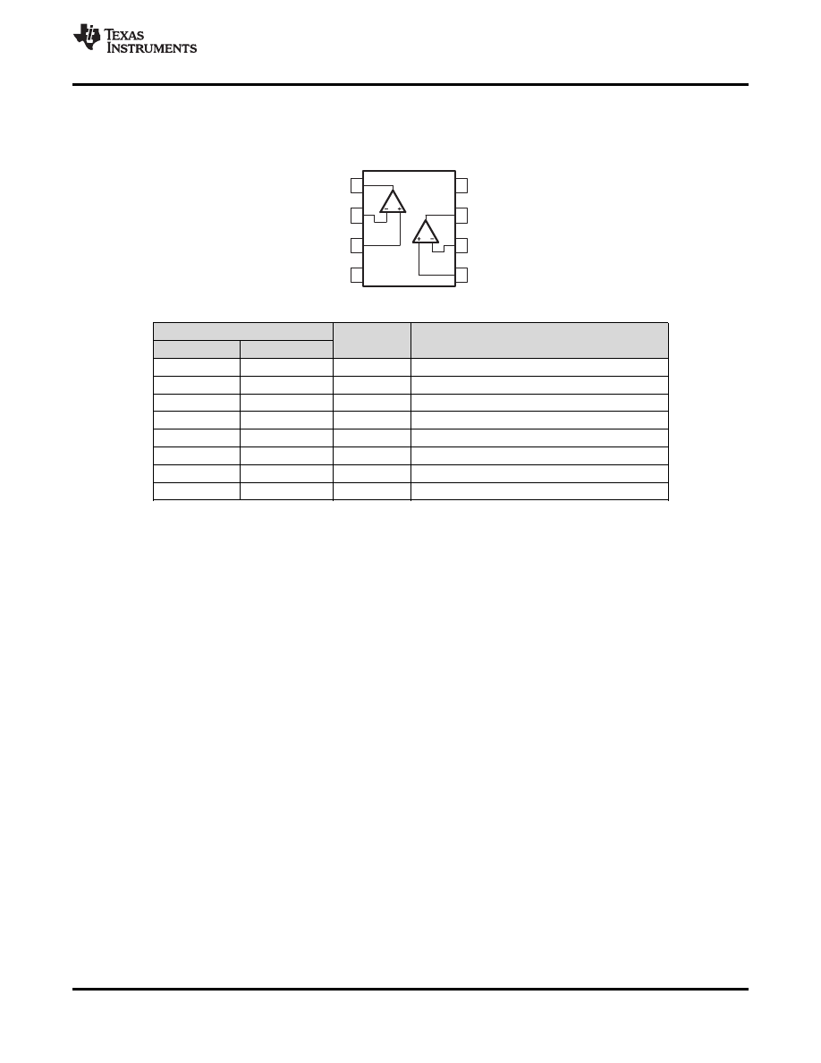
6 Pin Configuration and Functions
Pin Functions
PIN
TYPE
DESCRIPTION
NAME
NO.
IN1+
3
Input
Noninverting input
IN1-
2
Input
Inverting Input
IN2+
5
Input
Noninverting input
IN2-
6
Input
Inverting Input
OUT1
1
Output
Output 1
OUT2
7
Output
Output 2
V
CC+
8
Positive Supply
V
CC-
4
Negative Supply
Copyright © 2010-2014, Texas Instruments Incorporated
3
Product Folder Links:
SLOS481B - JULY 2010 - REVISED OCTOBER 2014
7 Specifications
7.1 Absolute Maximum Ratings
over operating free-air temperature range (unless otherwise noted)
(1)
MIN
MAX
UNIT
V
CC+
Supply voltage
(2)
18
V
V
CC-
Supply voltage
(2)
-18
V
V
CC+
- V
CC-
Supply voltage
36
V
Input voltage, either input
(2) (3)
V
CC-
V
CC+
V
Input current
(4)
±10
mA
Duration of output short circuit
(5)
Unlimited
T
J
Operating virtual junction temperature
150
°C
(1)
Stresses beyond those listed under Absolute Maximum Ratings may cause permanent damage to the device. These are stress ratings
only, and functional operation of the device at these or any other conditions beyond those indicated under Recommended Operating
Conditions is not implied. Exposure to absolute-maximum-rated conditions for extended periods may affect device reliability.
(2)
All voltage values, except differential voltages, are with respect to the midpoint between V
CC+
and V
CC-
.
(3)
The magnitude of the input voltage must never exceed the magnitude of the supply voltage.
(4)
Excessive input current will flow if a differential input voltage in excess of approximately 0.6 V is applied between the inputs, unless
some limiting resistance is used.
(5)
The output may be shorted to ground or either power supply. Temperature and/or supply voltages must be limited to ensure the
maximum dissipation rating is not exceeded.
7.2 Handling Ratings
PARAMETER
DEFINITION
MIN
MAX
UNIT
T
stg
Storage temperature range
-65
150
°C
Human-Body Model (HBM)
(1)
0
2.5
V
(ESD)
kV
Charged-Device Model (CDM)
(2)
0
1.5
(1)
JEDEC document JEP155 states that 500-V HBM allows safe manufacturing with a standard ESD control process.
(2)
JEDEC document JEP157 states that 250-V CDM allows safe manufacturing with a standard ESD control process.
7.3 Recommended Operating Conditions
MIN
MAX
UNIT
V
CC-
-5
-18
Supply voltage
V
V
CC+
5
18
T
A
Operating free-air temperature range
-40
85
°C
7.4 Thermal Information
LM833
THERMAL METRIC
(1)
D
DGK
P
UNIT
8 PINS
R
Θ
JA
Junction-to-ambient thermal resistance
(2) (3)
97
172
85
°C/W
(1)
For more information about traditional and new thermal metrics, see the IC Package Thermal Metrics application report (
).
(2)
Maximum power dissipation is a function of T
J
(max),
Θ
JA
, and T
A
. The maximum allowable power dissipation at any allowable ambient
temperature is P
D
= (T
J
(max) - T
A
) /
Θ
JA
. Operating at the absolute maximum T
J
of 150 °C can affect reliability.
(3)
The package thermal impedance is calculated in accordance with JESD 51-7.
4
Copyright © 2010-2014, Texas Instruments Incorporated
Product Folder Links:
SLOS481B - JULY 2010 - REVISED OCTOBER 2014
7.5 Electrical Characteristics
V
CC-
= -15 V, V
CC+
= 15 V, T
A
= 25 °C (unless otherwise noted)
PARAMETER
TEST CONDITIONS
MIN
TYP
MAX
UNIT
T
A
= 25 °C
0.15
2
V
IO
Input offset voltage
V
O
= 0, R
S
= 10
Ω¦, V
CM
= 0
mV
T
A
= -40 °C to 85 °C
3
Input offset voltage
αV
IO
V
O
= 0, R
S
= 10
Ω¦, V
CM
= 0
T
A
= -40 °C to 85 °C
2
μV/ °C
temperature coefficient
T
A
= 25 °C
300
750
I
IB
Input bias current
V
O
= 0, V
CM
= 0
nA
T
A
= -40 °C to 85 °C
800
T
A
= 25 °C
25
150
I
IO
Input offset current
V
O
= 0, V
CM
= 0
nA
T
A
= -40 °C to 85 °C
175
Common-mode input voltage
V
ICR
ΔV
IO
= 5 mV, V
O
= 0
±13
±14
V
range
T
A
= 25 °C
90
110
Large-signal differential
A
VD
R
L
≥ 2 kΩ¦, V
O
= ±10 V
dB
voltage amplification
T
A
= -40 °C to 85 °C
85
V
OM+
10.7
R
L
= 600
Ω¦
V
OM-
-11.9
V
OM+
13.2
13.8
Maximum output voltage
V
OM
V
ID
= ±1 V
R
L
= 2000
Ω¦
V
swing
V
OM-
-13.2
-13.7
V
OM+
13.5
14.1
R
L
= 10,000
Ω¦
V
OM-
-14
-14.6
CMMR
Common-mode rejection ratio
V
IN
= ±13 V
80
100
dB
k
SVR
(1)
Supply-voltage rejection ratio
V
CC+
= 5 V to 15 V, V
CC-
= -5 V to -15 V
80
105
dB
Source current
15
29
I
OS
Output short-circuit current
|V
ID
| = 1 V, Output to GND
mA
Sink current
-20
-37
T
A
= 25 °C
2.05
2.5
I
CC
Supply current (per channel)
V
O
= 0
mA
T
A
= -40 °C to 85 °C
2.75
(1)
Measured with V
CC ±
differentially varied at the same time
7.6 Operating Characteristics
V
CC-
= -15 V, V
CC+
= 15 V, T
A
= 25 °C (unless otherwise noted)
PARAMETER
TEST CONDITIONS
MIN
TYP
MAX
UNIT
SR
Slew rate at unity gain
A
VD
= 1, V
IN
= -10 V to 10 V, R
L
= 2 k
Ω¦, C
L
= 100 pF
5
7
V/
μs
GBW
Gain bandwidth product
f = 100 kHz
10
16
MHz
B
1
Unity gain frequency
Open loop
9
MHz
C
L
= 0 pF
-11
G
m
Gain margin
R
L
= 2 k
Ω¦
dB
C
L
= 100 pF
-6
C
L
= 0 pF
55
Φ
m
Phase margin
R
L
= 2 k
Ω¦
degrees
C
L
= 100 pF
40
Amp-to-amp isolation
f = 20 Hz to 20 kHz
-120
dB
Power bandwidth
V
O
= 27 V
(PP)
, R
L
= 2 k
Ω¦, THD ≤ 1%
120
kHz
THD
Total harmonic distortion
V
O
= 3 V
rms
, A
VD
= 1, R
L
= 2 k
Ω¦, f = 20 Hz to 20 kHz
0.002%
z
o
Open-loop output impedance
V
O
= 0, f = 9 MHz
37
Ω¦
r
id
Differential input resistance
V
CM
= 0
175
k
Ω¦
C
id
Differential input capacitance
V
CM
= 0
12
pF
V
n
Equivalent input noise voltage
f = 1 kHz, R
S
= 100
Ω¦
4.5
nV/
√Hz
I
n
Equivalent input noise current
f = 1 kHz
0.5
pA/
√Hz
Copyright © 2010-2014, Texas Instruments Incorporated
5
Product Folder Links:
0
100
200
300
400
500
600
-15
-10
-5
0
5
10
15
V
CM
- Common Mode Voltage - V
I
IB
-
In
p
u
t
B
ia
s
C
u
rr
e
n
t
-
n
A
V
CC+
= 15 V
V
CC-
= -15 V
T
A
= 25 °C
0
100
200
300
400
500
600
5
6
7
8
9
10 11 12 13 14 15 16 17 18
V
CC+
/-V
CC-
- Supply Voltage - V
I
IB
-
In
p
u
t
B
ia
s
C
u
rr
e
n
t
-
n
A
V
CM
= 0 V
T
A
= 25 °C
D.U.T.
Voltage Gain = 50,000
Scope
x 1
R
IN
= 1.0 M٦
+
-
100 k٦
10 Ω¦
0.1 µF
100 k٦
0.1 µF
24.3 k٦
4.7 µF
2.0 k٦
2.2 µF
22 µF
110 k٦
4.3 k٦
1/2
LM833
NOTE: All capacitors are non-polarized.
SLOS481B - JULY 2010 - REVISED OCTOBER 2014
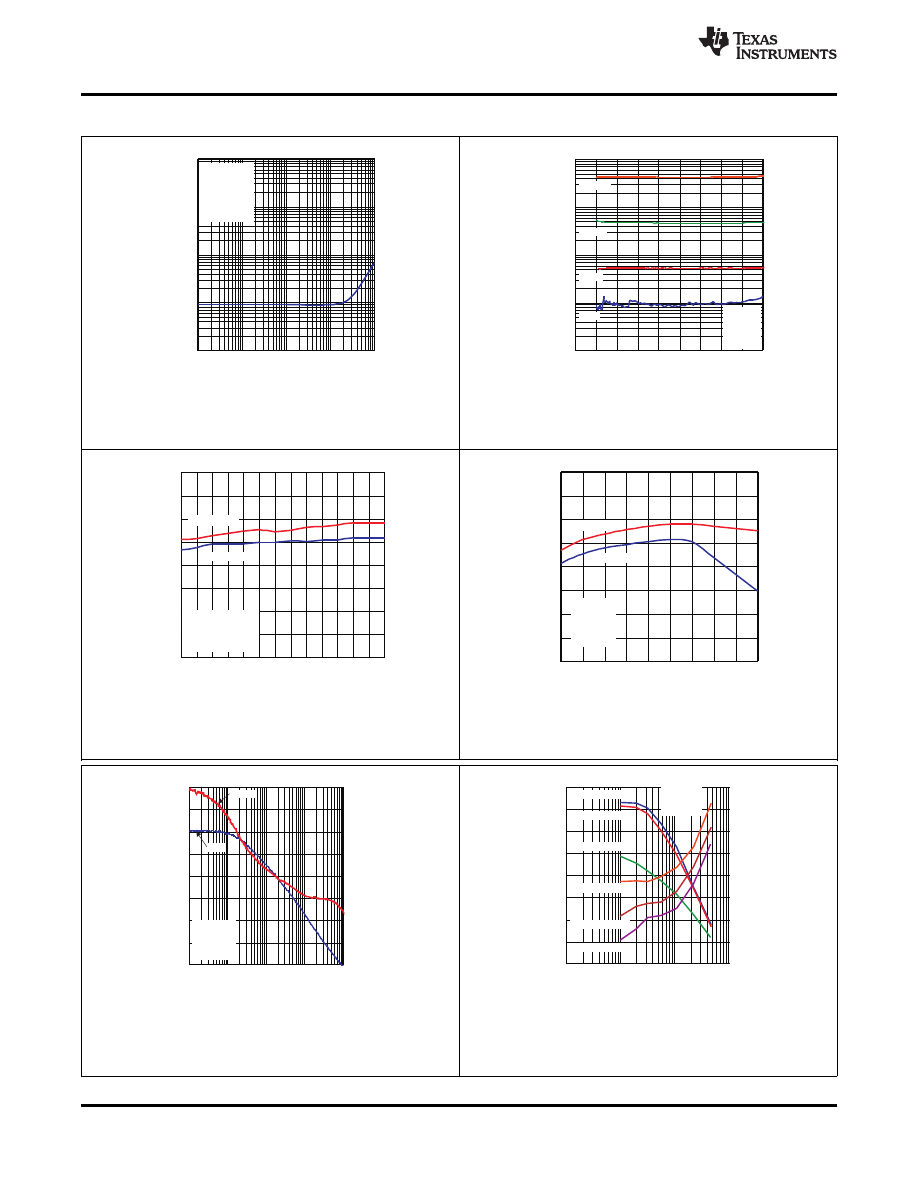
7.7 Typical Characteristics
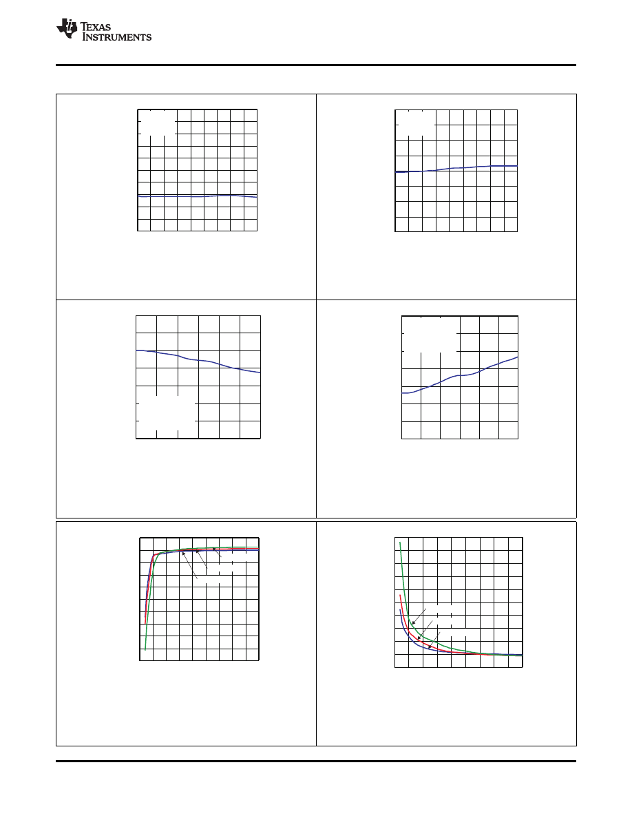
Figure 1. Voltage Noise Test Circuit (0.1 Hz to 10 Hz)
Figure 2. Input Bias Current vs Common-Mode Voltage
Figure 3. Input Bias Current vs Supply Voltage
6
Copyright © 2010-2014, Texas Instruments Incorporated
Product Folder Links:
0
1
2
3
4
5
6
7
8
9
10
0
0.5
1
1.5
2
2.5
3
3.5
4
4.5
R
L
- Load Resistance - k@
O
u
tp
u
t
S
a
tu
ra
ti
o
n
V
o
lt
a
g
e
P
ro
x
im
it
y
to
V
C
C
-
-
V
T = -55 °C
A
T = 25 °C
A
T = 125 °C
A
kW
-10
-9
-8
-7
-6
-5
-4
-3
-2
-1
0
0
0.5
1
1.5
2
2.5
3
3.5
4
4.5
R
L
- Load Resistance - kh
O
u
tp
u
t
S
a
tu
ra
ti
o
n
V
o
lt
a
g
e
P
ro
x
im
it
y
to
V
C
C
+
-
V
T = -55 °C
A
T = 25 °C
A
T = 125 °C
A
kW
-1.4
-1.2
-1
-0.8
-0.6
-0.4
-0.2
0
-55
-25
5
35
65
95
125
T
A
- Temperature - °C
In
p
u
t
C
o
m
m
o
n
-M
o
d
e
V
o
lt
a
g
e
H
ig
h
P
ro
x
im
it
y
to
V
C
C
+
-
V
V
CC+
= 3 V to 15 V
V
CC-
= -3 V to -15 V
V
IO
= 5 mV
V
O
= 0 V
D
0
0.2
0.4
0.6
0.8
1
1.2
1.4
-55
-25
5
35
65
95
125
T
A
- Temperature - °C
In
p
u
t
C
o
m
m
o
n
-M
o
d
e
V
o
lt
a
g
e
L
o
w
P
ro
x
im
it
y
to
V
C
C
-
-
V
V
CC+
= 3 V to 15 V
V
CC-
= -3 V to -15 V
è
V
IO
= 5 mV
V
O
= 0 V
D
-2
-1.5
-1
-0.5
0
0.5
1
1.5
2
-55
-35
-15
5
25
45
65
85
105 125
T
A
- Temperature - °C
V
IO
-
In
p
u
t
O
ff
s
e
t
V
o
lt
a
g
e
-
m
V
V
CC+
= 15 V
V
CC-
= -15 V
V
CM
= 0 V
0
100
200
300
400
500
600
700
800
900
1000
-55 -35
-15
5
25
45
65
85
105 125
T
A
- Temperature - °C
I
IB
-
In
p
u
t
B
ia
s
C
u
rr
e
n
t
-
n
A
V
CC+
= 15 V
V
CC-
= -15 V
V
CM
= 0 V
SLOS481B - JULY 2010 - REVISED OCTOBER 2014
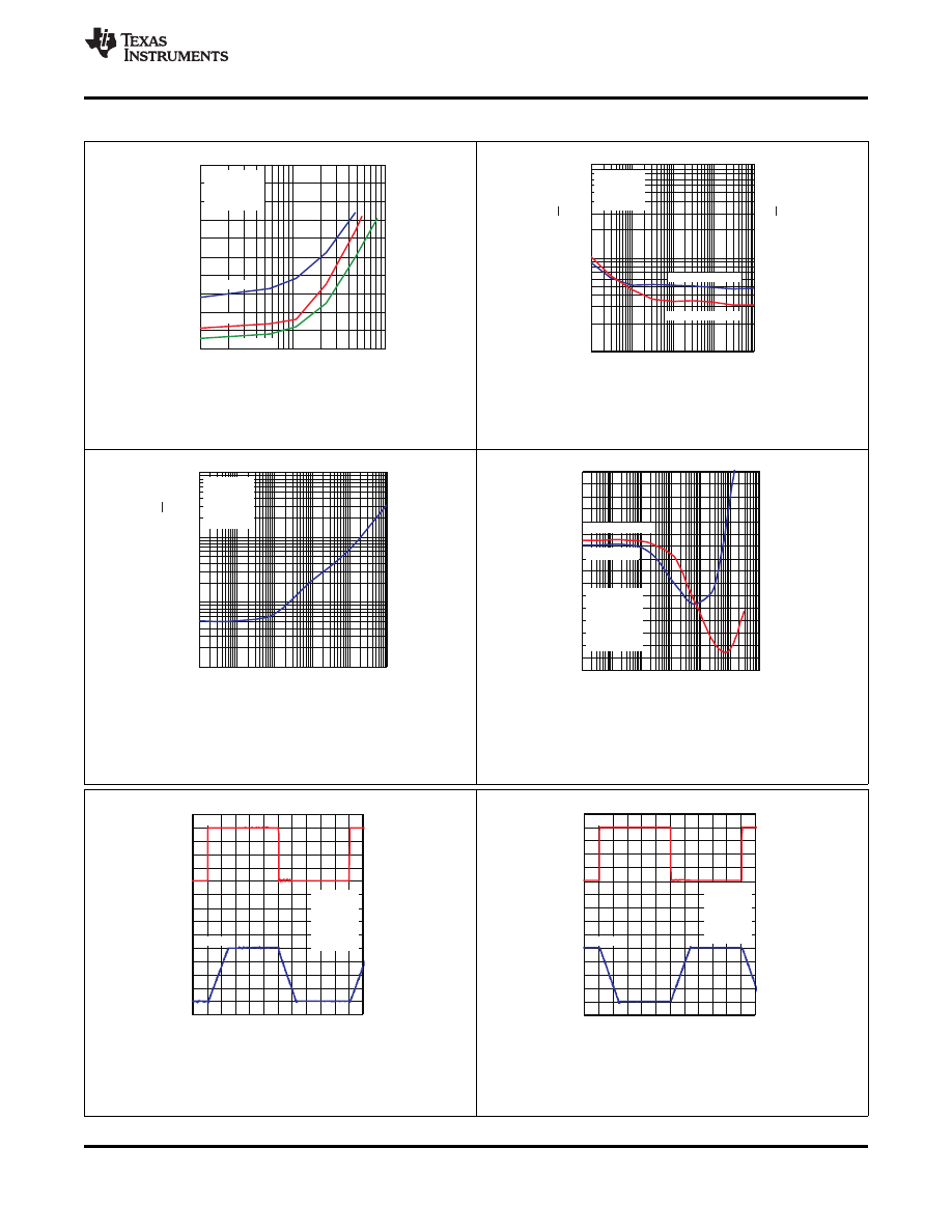
Typical Characteristics (continued)
Figure 4. Input Bias Current vs Temperature
Figure 5. Input Offset Voltage vs Temperature
Figure 6. Input Common-Mode Voltage Low Proximity
Figure 7. Input Common-Mode Voltage High Proximity
to V
CC-
vs Temperature
to V
CC+
vs Temperature
Figure 8. Output Saturation Voltage Proximity to V
CC+
Figure 9. Output Saturation Voltage Proximity to V
CC-
vs Load Resistance
vs Load Resistance
Copyright © 2010-2014, Texas Instruments Incorporated
7
Product Folder Links:
0
5
10
15
20
25
30
-55
-35
-15
5
25
45
65
85
105
125
T
A
- Temperature - °C
G
B
W
-
G
a
in
B
a
n
d
w
id
th
P
ro
d
u
c
t
-
M
H
z
0
5
10
15
20
25
30
5
6
7
8
9 10 11 12 13 14 15 16 17 18
V
CC+
/-V
CC-
- Supply Voltage - V
G
B
W
-
G
a
in
d
B
a
n
d
w
id
th
P
ro
d
u
c
t
-
M
H
z
0
10
20
30
40
50
60
70
80
90
100
1.0E+02 1.0E+03 1.0E+04 1.0E+05 1.0E+06 1.0E+07
f - Frequency - Hz
C
M
M
R
-
d
B
100
1k
10k
100k
1M
10M
V
= 15 V
V
= -15 V
V
= 0 V
V
= 1.5 V
T = 25 °C
CC+
CC-
CM
CM
A
D
±
0
10
20
30
40
50
60
70
80
90
100
110
120
1.0E+02 1.0E+03 1.0E+04 1.0E+05 1.0E+06 1.0E+07
f - Frequency - Hz
P
S
R
R
-
d
B
100
1k
10k
100k
1M
10M
V
= 15 V
V
= -15 V
T = 25 °C
CC+
CC-
A
T3P
T3N
10
20
30
40
50
60
70
-55
-35
-15
5
25
45
65
85
105
125
T
A
- Temperature - °C
I
O
S
-
O
u
tp
u
t
S
h
o
rt
-C
ir
c
u
it
C
u
rr
e
n
t
-
m
A
V
CC+
= 15 V
V
CC-
= -15 V
V
ID
= 1 V
Sink
Source
0
1
2
3
4
5
6
7
8
9
10
-55
-35
-15
5
25
45
65
85
105 125
T
A
- Temperature - °C
I
C
C
-
S
u
p
p
ly
C
u
rr
e
n
t
-
m
A
V
CM
= 0 V
R
L
= High Impedance
V
O
= 0 V
V
= 15 V
CC ±
±
V
= 10 V
CC ±
±
V
= 5 V
CC ±
±
SLOS481B - JULY 2010 - REVISED OCTOBER 2014
Typical Characteristics (continued)
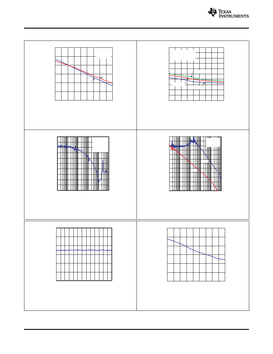
Figure 10. Output Short-Circuit Current vs Temperature
Figure 11. Supply Current vs Temperature
Figure 12. CMRR vs Frequency
Figure 13. PSSR vs Frequency
Figure 14. Gain Bandwidth Product vs Supply Voltage
Figure 15. Gain Bandwidth Product vs Temperature
8
Copyright © 2010-2014, Texas Instruments Incorporated
Product Folder Links:
0
5
10
15
20
25
30
35
40
45
50
1.0E+03
1.0E+04
1.0E+05
1.0E+06
1.0E+07
f - Frequency - Hz
Z
O
-
O
u
tp
u
t
Im
p
e
d
a
n
c
e
-
V
CC+
= 15 V
V
CC-
= -15 V
V
O
= 1 V
rms
T
A
= 25 °C
W
1k
10k
100k
1M
10M
A = 1
V
A = 10
V
A = 100
V
A = 1000
V
100
110
120
130
140
150
160
170
180
190
200
1.E+01
1.E+02
1.E+03
1.E+04
1.E+05
f - Frequency - Hz
C
ro
s
s
ta
lk
R
e
je
c
ti
o
n
-
d
B
1k
10k
100k
Drive Channel
V
= 15 V
V
= -15 V
R = 2 k
V = 20 V
T = 25 °C
CC+
CC-
L
O
PP
A
W
10
100
80
85
90
95
100
105
110
5
6
7
8
9 10 11 12 13 14 15 16 17 18
V
CC+
/-V
CC-
- Supply Voltage - V
A
V
-
O
p
e
n
-L
o
o
p
G
a
in
-
d
B
R = 2 k
f < 10 Hz
V = 2/3(V
- V
)
T = 25 °C
L
O
CC+
CC-
A
W
D
80
85
90
95
100
105
110
115
120
-55
-35
-15
5
25
45
65
85
105 125
T
A
- Temperature - °C
A
V
-
O
p
e
n
-L
o
o
p
G
a
in
-
d
B
R = 2 k
f < 10 Hz
V = 2/3(V
- V
)
T = 25 °C
L
O
CC+
CC-
A
W
D
0
5
10
15
20
25
30
1.E+01 1.E+02 1.E+03 1.E+04 1.E+05 1.E+06 1.E+07
f - Frequency - Hz
V
O
-
O
u
tp
u
t
V
o
lt
a
g
e
-
V
100
1k
10k
100k
1M
10M
10
V
= 15 V
V
= -15 V
R = 2 k
A = 1
THD < 1%
T = 25 °C
CC+
CC-
L
V
A
W
-20
-15
-10
-5
0
5
10
15
20
5
6
7
8
9
10 11 12 13 14 15 16 17 18
V
CC+
/-V
CC-
- Supply Voltage - V
V
O
-
O
u
tp
u
t
V
o
lt
a
g
e
-
V
R = 10 k
L
W
R = 2 k
L
W
R = 10 k
L
W
R = 2 k
L
W
SLOS481B - JULY 2010 - REVISED OCTOBER 2014
Typical Characteristics (continued)
Figure 16. Output Voltage vs Supply Voltage
Figure 17. Output Voltage vs Frequency
Figure 18. Open-Loop Gain vs Supply Voltage
Figure 19. Open-Loop Gain vs Temperature
Figure 20. Output Impedance vs Frequency
Figure 21. Crosstalk Rejection vs Frequency
Copyright © 2010-2014, Texas Instruments Incorporated
9
Product Folder Links:
0
10
20
30
40
50
60
70
80
1.E+03
1.E+04
1.E+05
1.E+06
1.E+07
f - Frequency - Hz
G
a
in
-
d
B
-180
-135
-90
-45
0
P
h
a
s
e
S
h
if
t
-
d
e
g
V
= 15 V
V
= -15 V
CC+
CC-
R = 2 k
T = 25 °C
L
A
W
100k
1M
10M
1k
10k
Phase
Gain
0
3
6
9
12
1
10
100
1000
C
out
- Output Load Capacitance - pF
G
a
in
M
a
rg
in
-
d
B
0
10
20
30
40
50
60
70
80
P
h
a
s
e
M
a
rg
in
-
d
e
g
Gain, T = 125 °C
A
Gain, T = 25 °C
A
Gain, T = -55 °C
A
Phase, T = 125 °C
A
Phase, T = 25 °C
A
Phase, T = -55 °C
A
V
= 15 V
V
= -15 V
CC+
CC-
V = 0 V
O
2
3
4
5
6
7
8
9
10
-55
-35
-15
5
25
45
65
85
105
125
T
A
- Temperature - °C
S
R
-
S
le
w
R
a
te
-
V
/ µ
s
V
= 15 V
V
= -15 V
CC+
CC-
V = 20 V
A = 1
R = 2 k
D
W
IN
V
L
Falling Edge
Rising Edge
2
3
4
5
6
7
8
9
10
5
6
7
8
9
10 11 12 13 14 15 16 17 18
V
CC+
/-V
CC-
- Supply Voltage - V
S
R
-
S
le
w
R
a
te
-
V
/ µ
s
Falling Edge
Rising Edge
V = 2/3(V
- V
)
A = 1
R = 2 k
T = 25 °C
D
W
IN
CC+
CC-
V
L
A
0.0001
0.001
0.01
0.1
1
0
1
2
3
4
5
6
7
8
9
V
O
- Output Voltage - V
rms
T
H
D
-
T
o
ta
l
H
a
rm
o
n
ic
D
is
to
rt
io
n
-
%
V
= 15 V
V
= -15 V
f = 2 kHz
R = 2 k
T = 25 °C
CC+
CC-
L
A
W
A = 1
V
A = 10
V
A = 100
V
A = 1000
V
0.0001
0.001
0.01
0.1
1
1.E+01
1.E+02
1.E+03
1.E+04
1.E+05
f - Frequency - Hz
T
H
D
-
T
o
ta
l
H
a
rm
o
n
ic
D
is
to
rt
io
n
-
%
1k
10k
100k
V
= 15 V
V
= -15 V
V = 1 V
A = 1
R = 2 k
T = 25 °C
CC+
CC-
O
rms
V
L
A
W
10
100
SLOS481B - JULY 2010 - REVISED OCTOBER 2014
Typical Characteristics (continued)
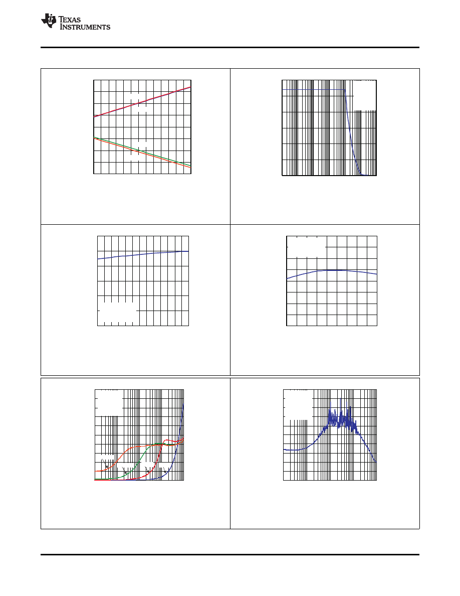
Figure 22. Total Harmonic Distortion vs Frequency
Figure 23. Total Harmonic Distortion vs Output Voltage
Figure 24. Slew Rate vs Supply Voltage
Figure 25. Slew Rate vs Temperature
Figure 26. Gain and Phase vs Frequency
Figure 27. Gain and Phase Margin
vs Output Load Capacitance
10
Copyright © 2010-2014, Texas Instruments Incorporated
Product Folder Links:
-15
-5
5
15
25
35
45
55
-2
2
6
10
14
18
22
Time - µs
V
O
-
O
u
tp
u
t
V
o
lt
a
g
e
-
V
-60
-50
-40
-30
-20
-10
0
10
V
I
-
In
p
u
t
V
o
lt
a
g
e
-
V
V
= 15 V
V
= -15 V
A = 1
R = 2 k
C
T = 25 °C
CC+
CC-
V
L
A
W
L
= 100 pF
Input
Output
-15
-5
5
15
25
35
45
55
-2
2
6
10
14
18
22
Time - µs
V
O
-
O
u
tp
u
t
V
o
lt
a
g
e
-
V
-60
-50
-40
-30
-20
-10
0
10
V
I
-
In
p
u
t
V
o
lt
a
g
e
-
V
V
= 15 V
V
= -15 V
A = -1
R = 2 k
C
T = 25 °C
CC+
CC-
V
L
A
W
L
= 100 pF
Input
Output
0
2
4
6
8
10
12
14
16
0
1
10
10 0
10 0 0
10 0 0 0
10 0 0 0 0
R
SD
- Differential Source Resistance - è
G
a
in
M
a
rg
in
-
d
B
0
4
8
12
16
2 0
2 4
2 8
3 2
3 6
4 0
4 4
4 8
5 2
5 6
6 0
6 4
P
h
a
s
e
M
a
rg
in
-
d
e
g
V
CC+
= 15 V
V
CC-
= -15 V
A
V
= 100
V
O
= 0 V
T
A
= 25 °C
Phase Margin
Gain Margin
W
1k
10k
100k
100
0
1
10
1
10
100
1000
1.E+01
1.E+02
1.E+03
1.E+04
1.E+05
1.E+06
R
S
- Source Resistance - è
In
p
u
t
R
e
fe
rr
e
d
N
o
is
e
V
o
lt
a
g
e
-
n
V
/r
tH
z
V
CC+
= 15 V
V
CC-
= -15 V
f = 1 Hz
T
A
= 25 °C
W
10
100
1k
10k
100k
nV/
Ã
Hz
1M
0
10
20
30
40
50
60
70
80
90
100
10
100
1000
C
out
- Output Load Capacitance - pF
O
v
e
rs
h
o
o
t
-
%
V
CC+
= 15 V
V
CC-
= -15 V
V
IN
= 100 mV
PP
T = 125 °C
A
T = 25 °C
A
T = -55 °C
A
1
10
100
10
100
1000
10000
100000
f - Frequency - Hz
In
p
u
t
V
o
lt
a
g
e
N
o
is
e
-
n
V
/r
tH
z
0.1
1
10
In
p
u
t
C
u
rr
e
n
t
N
o
is
e
-
p
A
/r
tH
z
V
CC+
= 15 V
V
CC-
= -15 V
T
A
= 25 °C
Input Voltage Noise
Input Current Noise
10
100
1k
10k
100k
pA/
ÃHz
nV/
ÃHz
SLOS481B - JULY 2010 - REVISED OCTOBER 2014
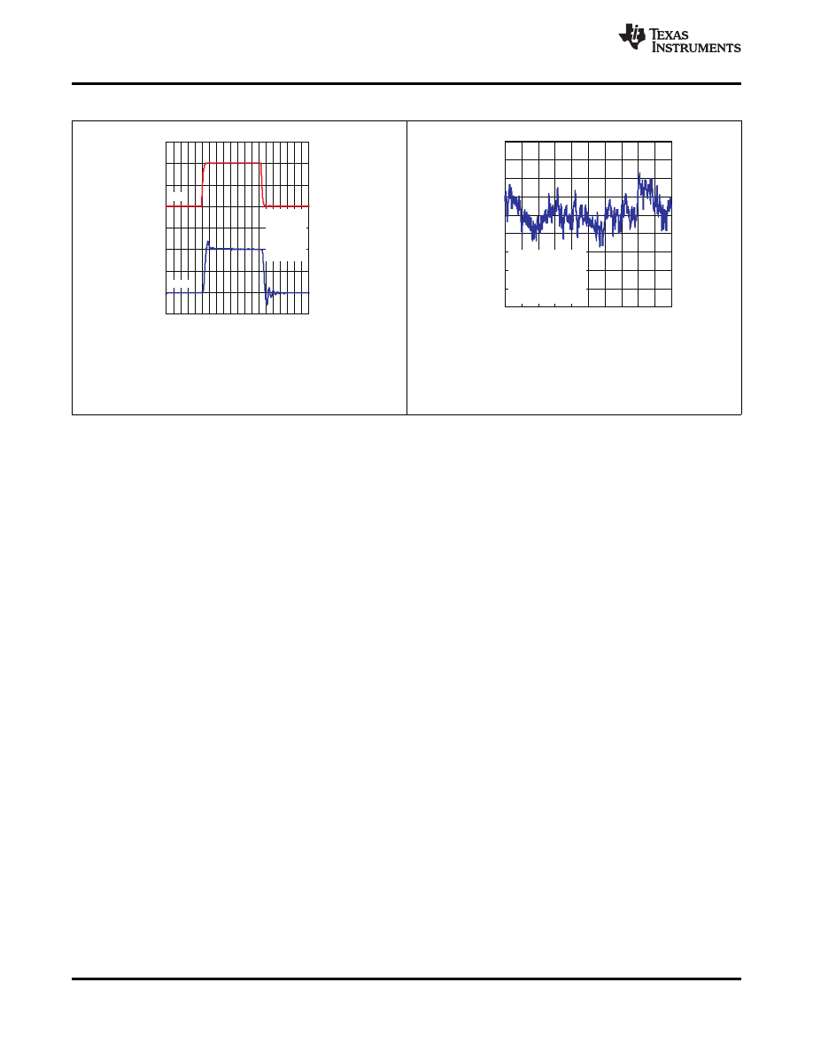
Typical Characteristics (continued)
Figure 28. Overshoot vs Output Load Capacitance
Figure 29. Input Voltage and Current Noise vs Frequency
Figure 30. Input Referred Noise Voltage
Figure 31. Gain and Phase Margin
vs Source Resistance
vs Differential Source Resistance
Figure 32. Large Signal Transient Response (A
V
= 1)
Figure 33. Large Signal Transient Response (A
V
= -1)
Copyright © 2010-2014, Texas Instruments Incorporated
11
Product Folder Links:
-0.2
-0.1
0
0.1
0.2
0.3
0.4
0.5
0.6
-0.5
0.0
0.5
1.0
1.5
Time - µs
V
O
-
O
u
tp
u
t
V
o
lt
a
g
e
-
V
-0.6
-0.5
-0.4
-0.3
-0.2
-0.1
0.0
0.1
0.2
V
I
-
In
p
u
t
V
o
lt
a
g
e
-
V
V
= 15 V
V
= -15 V
A = 1
R = 2 k
C
T = 25 °C
CC+
CC-
V
L
A
W
L
= 100 pF
Input
Output
-500
-400
-300
-200
-100
0
100
200
300
400
-5
-4
-3
-2
-1
0
1
2
3
4
5
Time - s
In
p
u
t
V
o
lt
a
g
e
N
o
is
e
-
n
V
T3
V
CC+
= 15 V
V
CC-
= -15 V
BW = 0.1 Hz to 10 Hz
T
A
= 25 °C
SLOS481B - JULY 2010 - REVISED OCTOBER 2014
Typical Characteristics (continued)
Figure 35. Low-Frequency Noise
Figure 34. Small Signal Transient Response
12
Copyright © 2010-2014, Texas Instruments Incorporated
Product Folder Links:
IN
Ã
IN+
VCC
VEE
VOUT
SLOS481B - JULY 2010 - REVISED OCTOBER 2014
8 Detailed Description
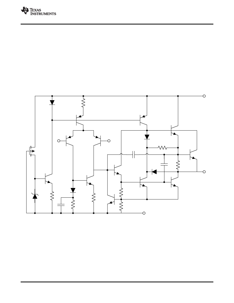
8.1 Overview
The LM833 device is a dual operational amplifier with high-performance specifications for use in quality audio
and data-signal applications. This device operates over a wide range of single- and dual-supply voltage with low
noise, high-gain bandwidth, and high slew rate. Additional features include low total harmonic distortion, excellent
phase and gain margins, large output voltage swing with no deadband crossover distortions, and symmetrical
sink/source performance. The dual amplifiers are utilized widely in circuit of audio optimized for all preamp and
high-level stages in PCM and HiFi systems. The LM833 device is pin-for-pin compatible with industry-standard
dual operation amplifiers' pin assignments. With addition of a preamplifier, the gain of the power stage can be
greatly reduced to improve performance.
8.2 Functional Block Diagram
Copyright © 2010-2014, Texas Instruments Incorporated
13
Product Folder Links:

SLOS481B - JULY 2010 - REVISED OCTOBER 2014
8.3 Feature Description
8.3.1 Operating Voltage
The LM833 operational amplifier is fully specified and ensured for operation from ±5 V to ±18 V. In addition,
many specifications apply from -40 °C to 85 °C. Parameters that vary significantly with operating voltages or
temperature are shown in
.
8.3.2 High Gain Bandwidth Product
Gain bandwidth product is found by multiplying the measured bandwidth of an amplifier by the gain at which that
bandwidth was measured. The LM833 has a high gain bandwidth of 16 MHz which stays relatively stable over a
wide range of supply voltages. Parameters that vary significantly with temperature are shown in
.
8.3.3 Low Total Harmonic Distortion
Harmonic distortions to an audio signal are created by electronic components in a circuit. Total harmonic
distortion (THD) is a measure of harmonic distortions accumulated by a signal in an audio system. The LM833
has a very low THD of 0.002% meaning that the LM833 will add little harmonic distortion when used in audio
signal applications. More specific characteristics are shown in
8.4 Device Functional Modes
The LM833 is powered on when the supply is connected. It can be operated as a single supply operational
amplifier or dual supply amplifier depending on the application.
14
Copyright © 2010-2014, Texas Instruments Incorporated
Product Folder Links:
+
+
R
5
4.3 k
R
4
2 k
R
3
2.37
R
1
80.6 k
R
6
54.9 k
C
3
33 nF
C
1
39 nF
C
4
2
P
F
R
0
499
C
0
200
P
F
47 k
C
P
VIN
VOUT
-15 V
15 V
½ LM833
½ LM833
3
2
4
1
5
6
8
7
R
2
8.45 k
SLOS481B - JULY 2010 - REVISED OCTOBER 2014
9 Application and Implementation
NOTE
Information in the following applications sections is not part of the TI component
specification, and TI does not warrant its accuracy or completeness. TIs customers are
responsible for determining suitability of components for their purposes. Customers should
validate and test their design implementation to confirm system functionality.
9.1 Application Information
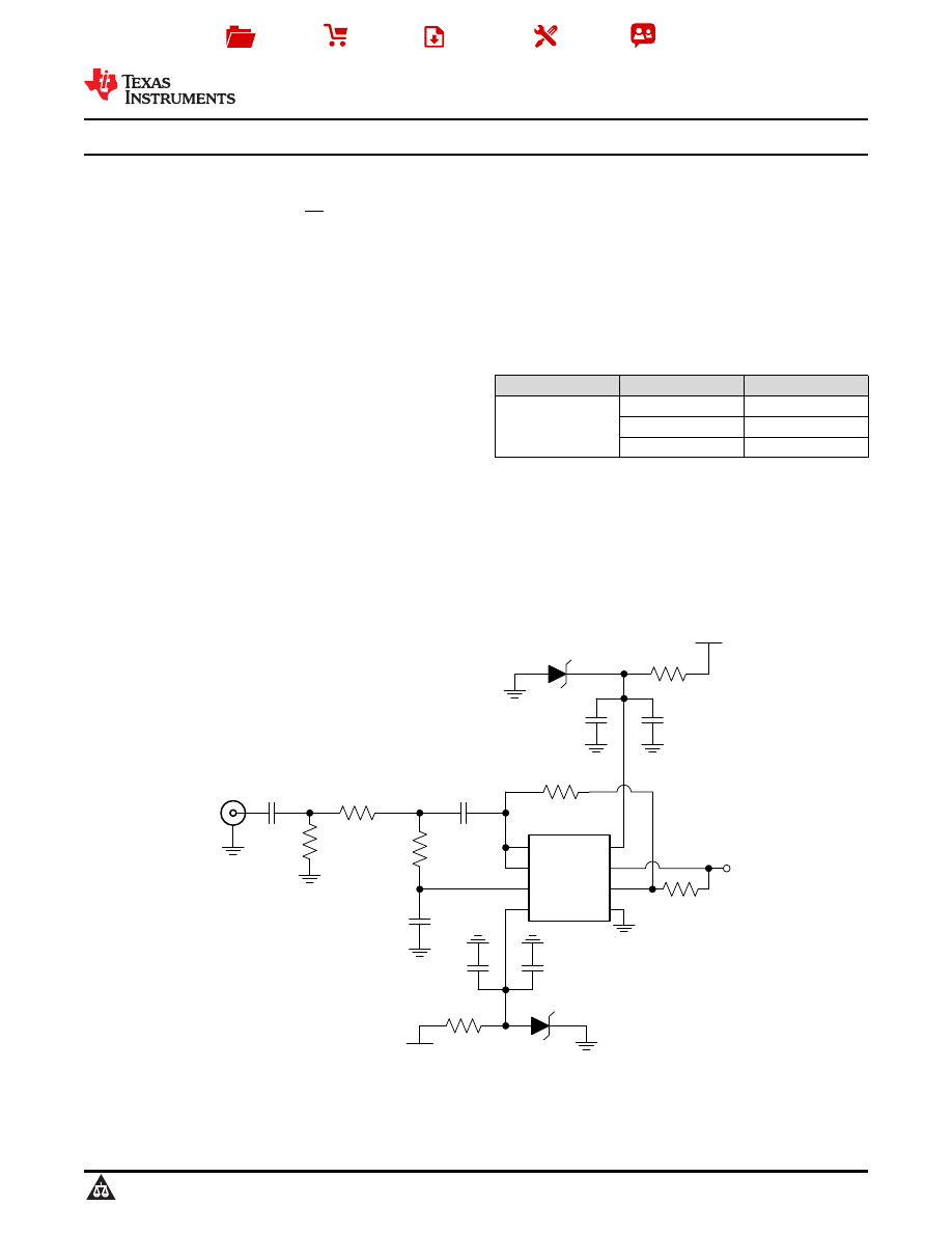
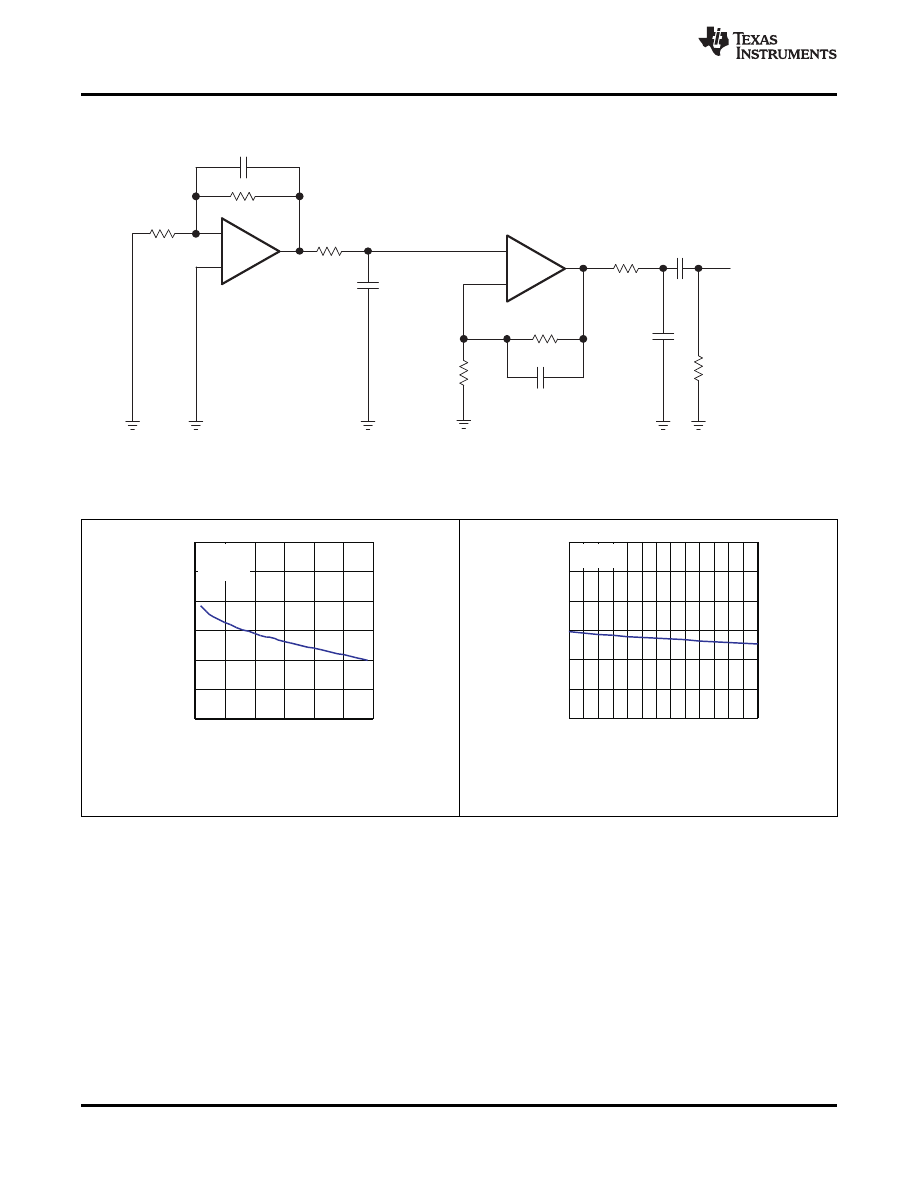
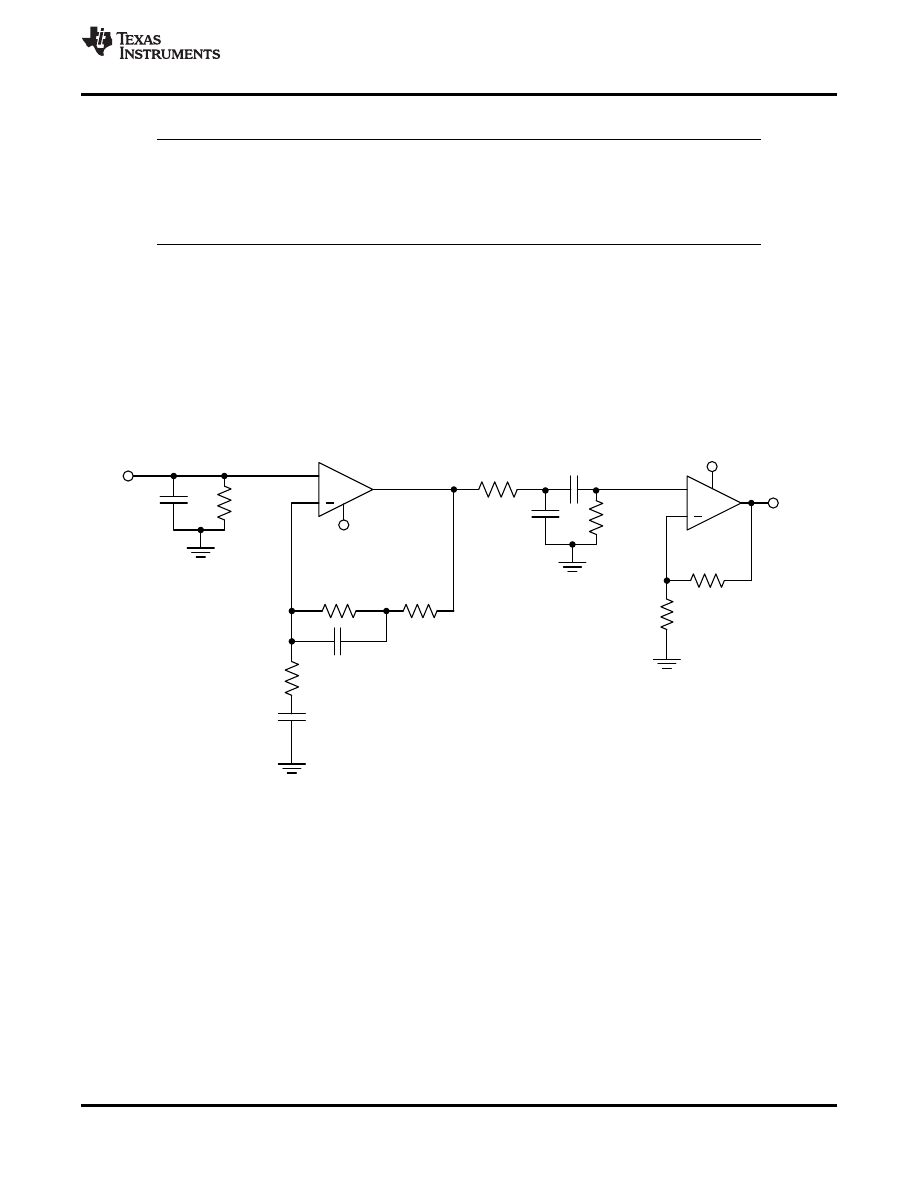
An application of the LM833 is the two stage RIAA Phono Preamplifier. A primary task of the phono preamplifier
is to provide gain (usually 30 to 40 dB at 1 kHz) and accurate amplitude and phase equalization to the signal
from a moving magnet or a moving coil cartridge. In addition to the amplification and equalization functions, the
phono preamp must not add significant noise or distortion to the signal from the cartridge. The circuit shown in
uses two amplifiers, fulfills these qualifications, and has greatly improved performance over a single-
amplifier design.
9.2 Typical Application
Figure 36. RIAA Phono Preamplifier
9.2.1 Design Requirements
Supply Voltage = ±15 V
Low-Frequency
-3 dB corner of the first amplifier (f
0
) > 20 Hz (below audible range)
Low-Frequency
-3 dB corner of the second stage (f
L
) = 20.2 Hz
9.2.2 Detailed Design Procedure
9.2.2.1 Introduction to Design Method
through
show the design equations for the preamplifier.
R
1
= 8.058 R
0
A
1
where
A
1
is the 1 kHz voltage gain of the first amplifier
(1)
Copyright © 2010-2014, Texas Instruments Incorporated
15
Product Folder Links:
3
1
4
3.18 10
Example : C
0.03946 F
8.058 10
-
´
=
=
m
´
3
1
1
3.18 10
Calculate C
R
-
´
=
0
0
0
1
C
2
f R
»
p
5
V 2
4
R
A
1
R
=
+
(
)
4
L
1
C
2
f
R3
R6
=
p
+
5
5
3
6
3
3
6
P
(R
R )
7.5 10
C
7.5 10
R R
R
-
-
+
´
=
´
=
1
2
0
R
R
R
9
=
-
3
1
1
3.18 10
C
R
-
´
=
SLOS481B - JULY 2010 - REVISED OCTOBER 2014
Typical Application (continued)
(2)
(3)
(4)
where
f
L
is the low-frequency
-3 dB corner of the second stage
(5)
For standard RIAA preamplifiers, f
L
should be kept well below the audible frequency range. If the preamplifier is
to follow the IEC recommendation (IEC Publication 98, Amendment #4), f
L
should equal 20.2 Hz.
where
A
V2
is the voltage gain of the second amplifier
(6)
where
f
0
is the low-frequency
-3 dB corner of the first amplifier
(7)
This should be kept well below the audible frequency range.
A design procedure is shown below with an illustrative example using 1% tolerance E96 components for close
conformance to the ideal RIAA curve. Because 1% tolerance capacitors are often difficult to find except in 5% or
10% standard values, the design procedure calls for re-calculation of a few component values so that standard
capacitor values can be used.
9.2.2.2 RIAA Phono Preamplifier Design Procedure
A design procedure is shown below with an illustrative example using 1% tolerance E96 components for close
conformance to the ideal RIAA curve. Since 1% tolerance capacitors are often difficult to find except in 5% or
10% standard values, the design procedure calls for re-calculation of a few component values so that standard
capacitor values can be used.
Choose R
0
. R
0
should be small for minimum noise contribution, but not so small that the feedback network
excessively loads the amplifier.
Example: Choose R
0
= 500
Choose 1 kHz gain, A
V1
of first amplifier. This will typically be around 20 dB to 30 dB.
Example: Choose A
V1
= 26 dB = 20
Calculate R
1
= 8.058 R
0
A
V1
Example: R
1
= 8.058 × 500 × 20 = 80.58 k
(8)
(9)
If C
1
is not a convenient value, choose the nearest convenient value and calculate a new R
1
from
16
Copyright © 2010-2014, Texas Instruments Incorporated
Product Folder Links:
5
P
3
5
P
8
7.5 10
Calculate R
C
7.5 10
Example: R
2.273k
3.3 10
-
-
-
´
=
´
=
=
´
1
2
0
4
2
R
Calculate R
R
9
8.06 10
Example : R
499
8456.56
9
=
-
´
=
-
=
4
0
8.06 10
Example: New R
498.8
8.058 20
´
=
=
´
1
0
V1
R
R
8.058 A
=
3
1
8
1
3.18 10
New R
81.54 k
3.9 10
Use R
80.6 k
-
-
´
=
=
´
=
3
1
1
3.18 10
R
C
-
´
=
SLOS481B - JULY 2010 - REVISED OCTOBER 2014
Typical Application (continued)
(10)
Example: New C
1
= 0.039
μF.
(11)
Calculate a new value for R
0
from
(12)
(13)
Use R
0
= 499.
(14)
Use R
2
= 8.45 K.
Choose a convenient value for C
3
in the range from 0.01
μF to 0.05 μF.
Example: C
3
= 0.033
μF
(15)
Choose a standard value for R
3
that is slightly larger than R
P
.
Example: R
3
= 2.37 k
Calculate R
6
from 1 / R
6
= 1 / R
P
- 1 / R
3
Example: R
6
= 55.36 k
Use 54.9 k
Calculate C
4
for low-frequency rolloff below 1 Hz from design
Example: C
4
= 2
μF. Use a good quality mylar, polystyrene, or polypropylene.
Choose gain of second amplifier.
Example: The 1 kHz gain up to the input of the second amplifier is about 26 dB for this example. For an
overall 1 kHz gain equal to about 36 dB we choose:
A
V2
= 10 dB = 3.16
Choose value for R4.
Example: R
4
= 2 k
Calculate R
5
= (A
V2
- 1) R
4
Copyright © 2010-2014, Texas Instruments Incorporated
17
Product Folder Links:
5 V
-5 V
15 V
-15 V
R
O
V
O
R = 2 k
L
Ω¦
C
L
SLOS481B - JULY 2010 - REVISED OCTOBER 2014
Typical Application (continued)
Example: R
5
= 4.32 k
Use R
5
= 4.3 k
Calculate C
0
for low-frequency rolloff below 1 Hz from design
Example: C
0
= 200
μF
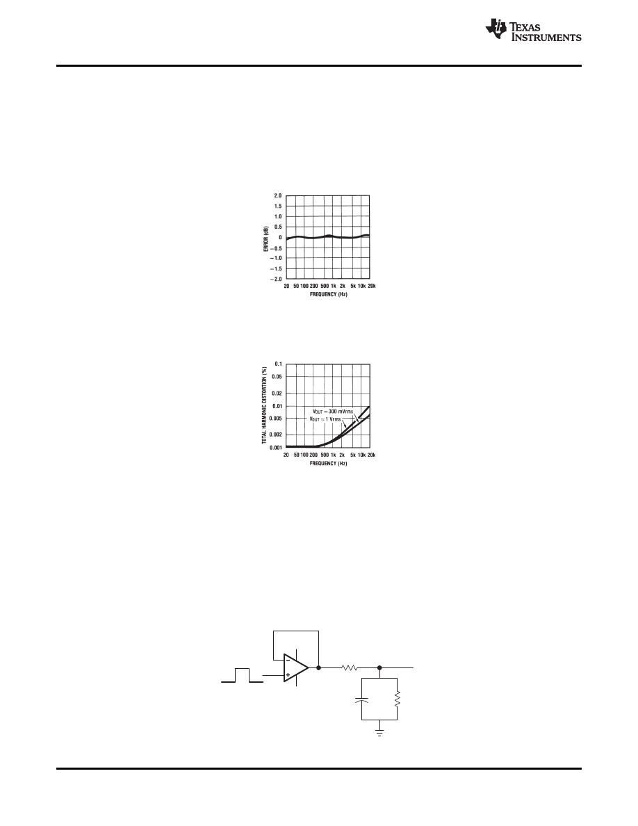
9.2.3 Application Curves for Output Characteristics
The maximum observed error for the prototype was 0.1 dB.
Figure 37. Deviation from Ideal RIAA Response for
Circuit of
Using 1% Resistors
The lower curve is for an output level of 300 mV
rms
and the upper curve is for an output level of 1 V
rms
.
Figure 38. THD of Circuit in
as a Function of Frequency
9.3 Typical Application Reducing Oscillation from High-Capacitive Loads
While all the previously stated operating characteristics are specified with 100-pF load capacitance, the LM833
device can drive higher-capacitance loads. However, as the load capacitance increases, the resulting response
pole occurs at lower frequencies, causing ringing, peaking, or oscillation. The value of the load capacitance at
which oscillation occurs varies from lot-to-lot. If an application appears to be sensitive to oscillation due to load
capacitance, adding a small resistance in series with the load should alleviate the problem (see
9.3.1 Test Schematic
Figure 39. Capacitive Load Testing Circuit
18
Copyright © 2010-2014, Texas Instruments Incorporated
Product Folder Links:
250 ns per Division
0.25
V per Division
250 ns per Division
0.25
V per Division
250 ns per Division
0.25
V per Division
250 ns per Division
0.25
V per Division
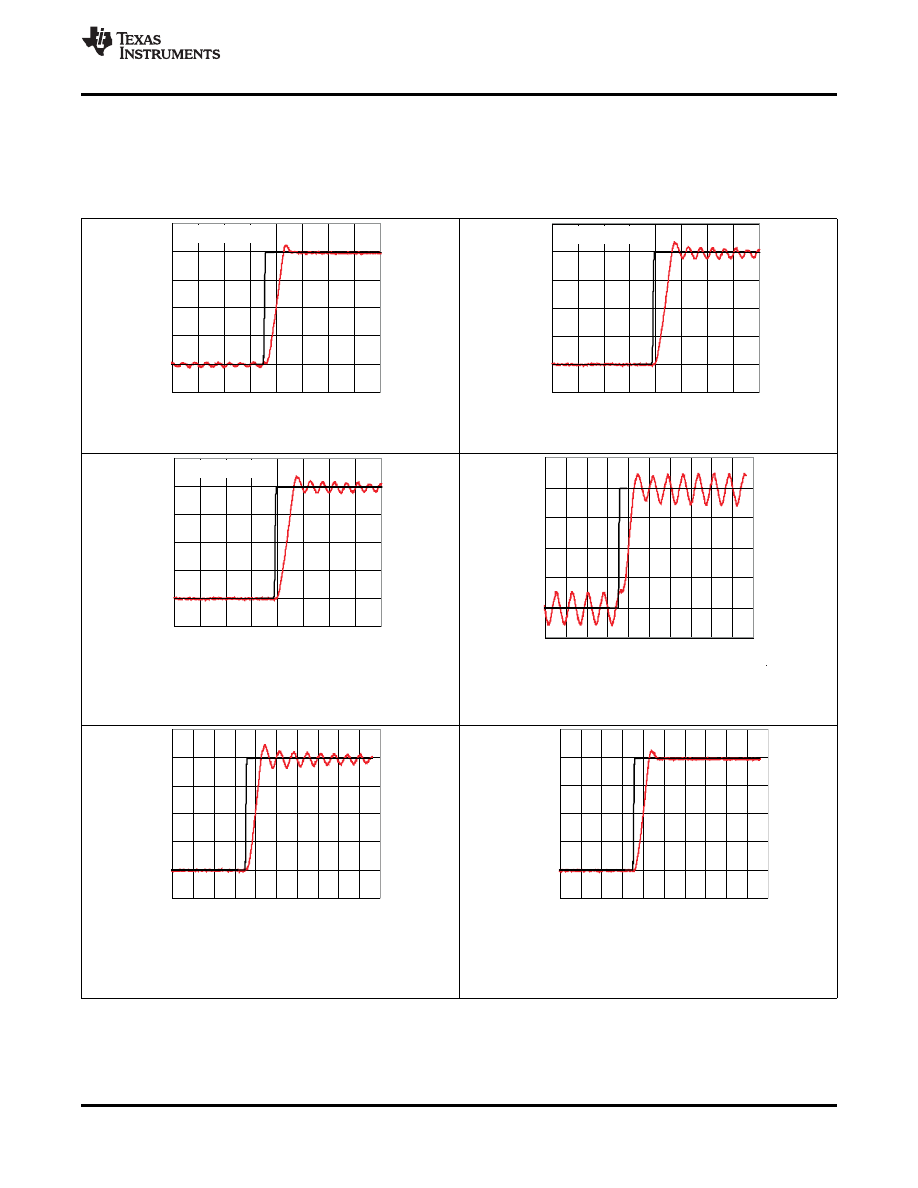
Maximum capacitance
before oscillation = 590 pF
0.25
V per Division
250 ns per Division
Maximum capacitance
before oscillation = 380 pF
250 ns per Division
0.25
V per Division
Maximum capacitance
before oscillation = 590 pF
SLOS481B - JULY 2010 - REVISED OCTOBER 2014
Typical Application Reducing Oscillation from High-Capacitive Loads (continued)
9.3.2 Output Characteristics
through
demonstrate the effect adding this small resistance has on the ringing in the output
signal.
Figure 40. Pulse Response
Figure 41. Pulse Response
(R
L
= 600
Ω¦, C
L
= 380 pF)
(R
L
= 2 k
Ω¦, C
L
= 560 pF)
Figure 42. Pulse Response
(R
L
= 10 k
Ω¦, C
L
= 590 pF)
Figure 43. Pulse Response
(R
O
= 0
Ω¦, C
O
= 1000 pF,
R
L
= 2 k
Ω¦)
Figure 44. Pulse Response
(R
O
= 4
Ω¦, C
O
= 1000 pF,
Figure 45. Pulse Response
R
L
= 2 k
Ω¦)
(R
O
= 35
Ω¦, C
O
= 1000 pF,
R
L
= 2 k
Ω¦)
Copyright © 2010-2014, Texas Instruments Incorporated
19
Product Folder Links:
+
RIN
RG
RF
VOUT
VIN
SLOS481B - JULY 2010 - REVISED OCTOBER 2014
10 Power Supply Recommendations
The LM833 is specified for operation from 10 to 36 V ( ±5 to ±18 V); many specifications apply from -40 °C to
85 °C. The
section presents parameters that can exhibit significant variance with regard to
operating voltage or temperature.
CAUTION
Supply voltages larger than 36 V can permanently damage the device (see
).
Place 0.1-
μF bypass capacitors close to the power-supply pins to reduce errors coupling in from noisy or high
impedance power supplies. For more detailed information on bypass capacitor placement, refer to the
section.
11 Layout
11.1 Layout Guidelines
For best operational performance of the device, use good PCB layout practices, including:
Noise can propagate into analog circuitry through the power pins of the circuit as a whole and the operational
amplifier. Bypass capacitors are used to reduce the coupled noise by providing low impedance power
sources local to the analog circuitry.
-
Connect low-ESR, 0.1-
μF ceramic bypass capacitors between each supply pin and ground, placed as
close to the device as possible. A single bypass capacitor from V+ to ground is applicable for single
supply applications.
Separate grounding for analog and digital portions of circuitry is one of the simplest and most-effective
methods of noise suppression. One or more layers on multilayer PCBs are usually devoted to ground planes.
A ground plane helps distribute heat and reduces EMI noise pickup. Make sure to physically separate digital
and analog grounds, paying attention to the flow of the ground current. For more detailed information, refer to
Circuit Board Layout Techniques, (
To reduce parasitic coupling, run the input traces as far away from the supply or output traces as possible. If
it is not possible to keep them separate, it is much better to cross the sensitive trace perpendicular as
opposed to in parallel with the noisy trace.
Place the external components as close to the device as possible. Keeping RF and RG close to the inverting
input minimizes parasitic capacitance, as shown in
Keep the length of input traces as short as possible. Always remember that the input traces are the most
sensitive part of the circuit.
Consider a driven, low-impedance guard ring around the critical traces. A guard ring can significantly reduce
leakage currents from nearby traces that are at different potentials.
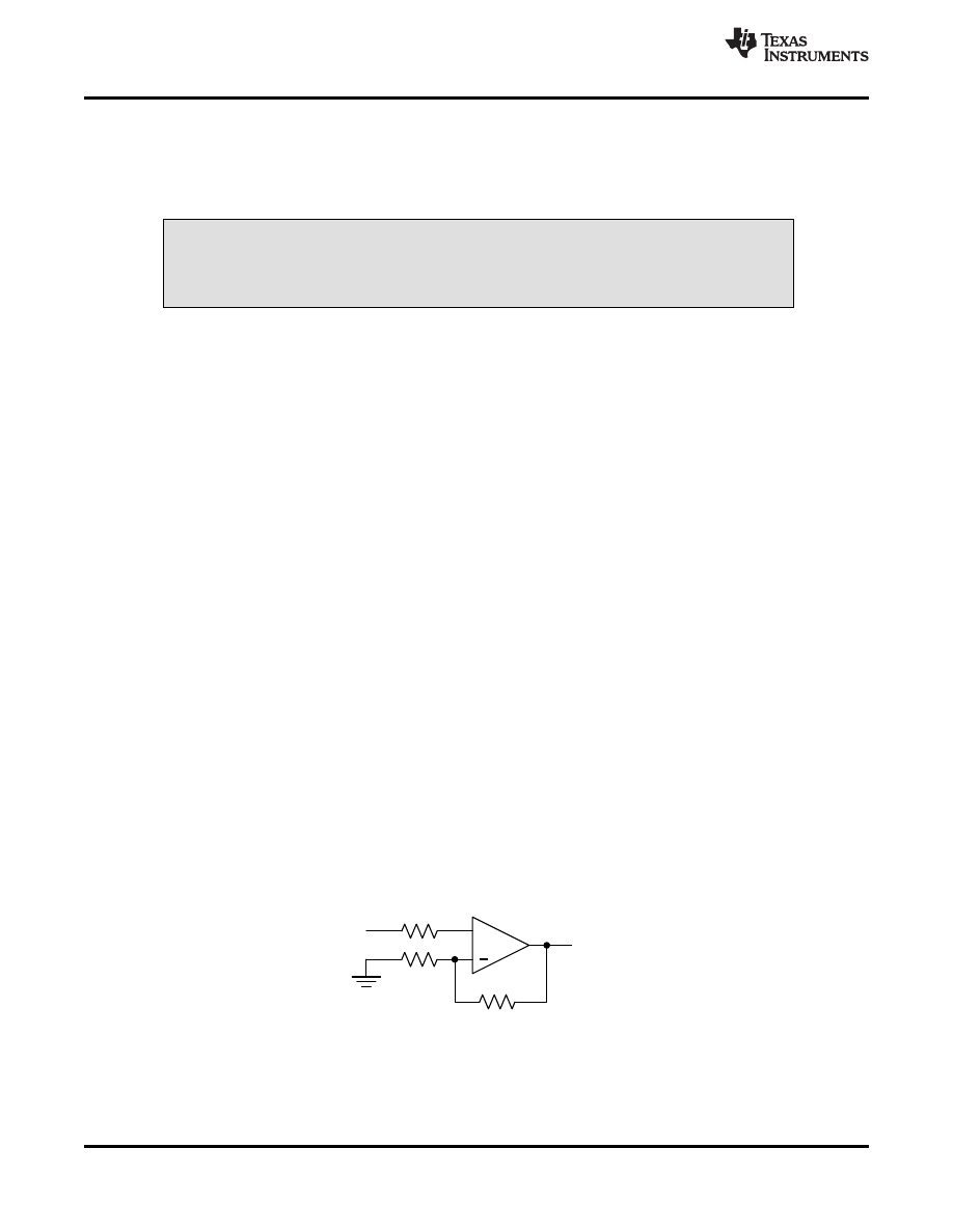
11.2 Layout Example
Figure 46. Operational Amplifier Schematic for Noninverting Configuration
20
Copyright © 2010-2014, Texas Instruments Incorporated
Product Folder Links:
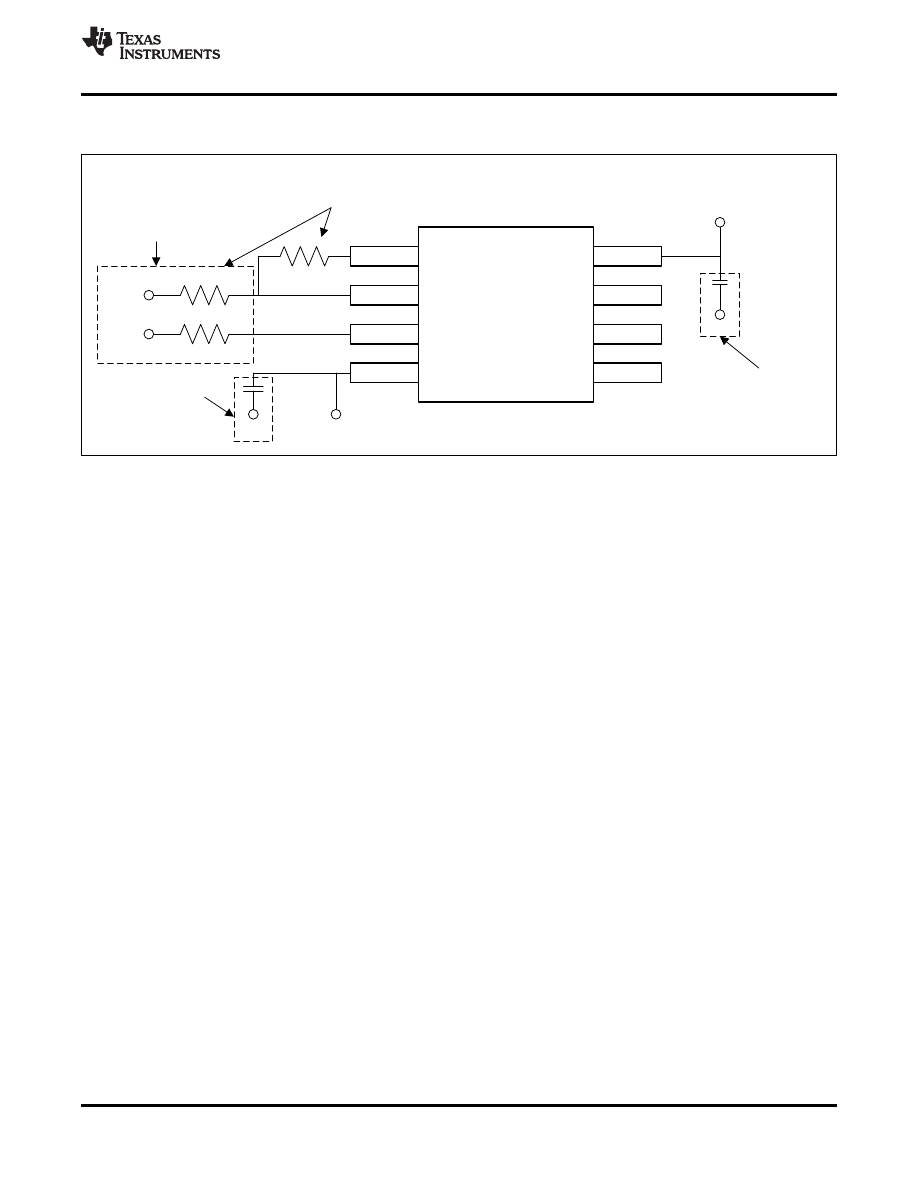
OUT1
OUT2
IN1
Ã
IN1+
VCC
Ã
VCC+
IN2
Ã
IN2+
RG
RIN
RF
GND
VIN
VS-
GND
VS+
GND
Run the input traces as far
away from the supply lines
as possible
Only needed for
dual-supply
operation
Place components close to
device and to each other to
reduce parasitic errors
Use low-ESR, ceramic
bypass capacitor
(or GND for single supply)
Ground (GND) plane on another layer
SLOS481B - JULY 2010 - REVISED OCTOBER 2014
Layout Example (continued)
Figure 47. Operational Amplifier Board Layout for Noninverting Configuration
Copyright © 2010-2014, Texas Instruments Incorporated
21
Product Folder Links:

SLOS481B - JULY 2010 - REVISED OCTOBER 2014
12 Device and Documentation Support
12.1 Trademarks
All trademarks are the property of their respective owners.
12.2 Electrostatic Discharge Caution
These devices have limited built-in ESD protection. The leads should be shorted together or the device placed in conductive foam
during storage or handling to prevent electrostatic damage to the MOS gates.
12.3 Glossary
TI Glossary.
This glossary lists and explains terms, acronyms, and definitions.
22
Copyright © 2010-2014, Texas Instruments Incorporated
Product Folder Links:

SLOS481B - JULY 2010 - REVISED OCTOBER 2014
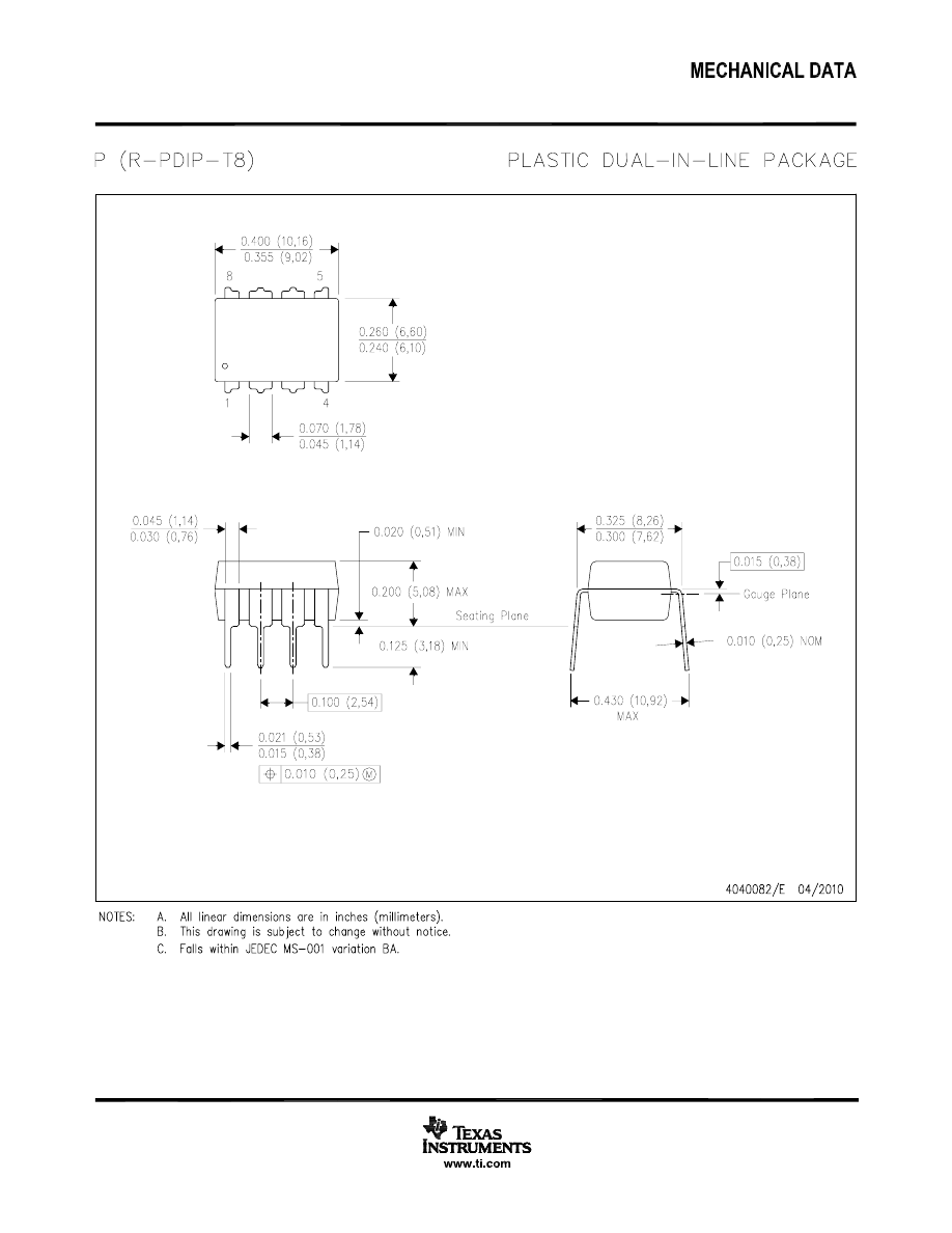
13 Mechanical, Packaging, and Orderable Information
The following pages include mechanical, packaging, and orderable information. This information is the most
current data available for the designated devices. This data is subject to change without notice and revision of
this document. For browser-based versions of this data sheet, refer to the left-hand navigation.
Copyright © 2010-2014, Texas Instruments Incorporated
23
Product Folder Links:
PACKAGE OPTION ADDENDUM
www.ti.com
21-Jan-2014
Addendum-Page 1
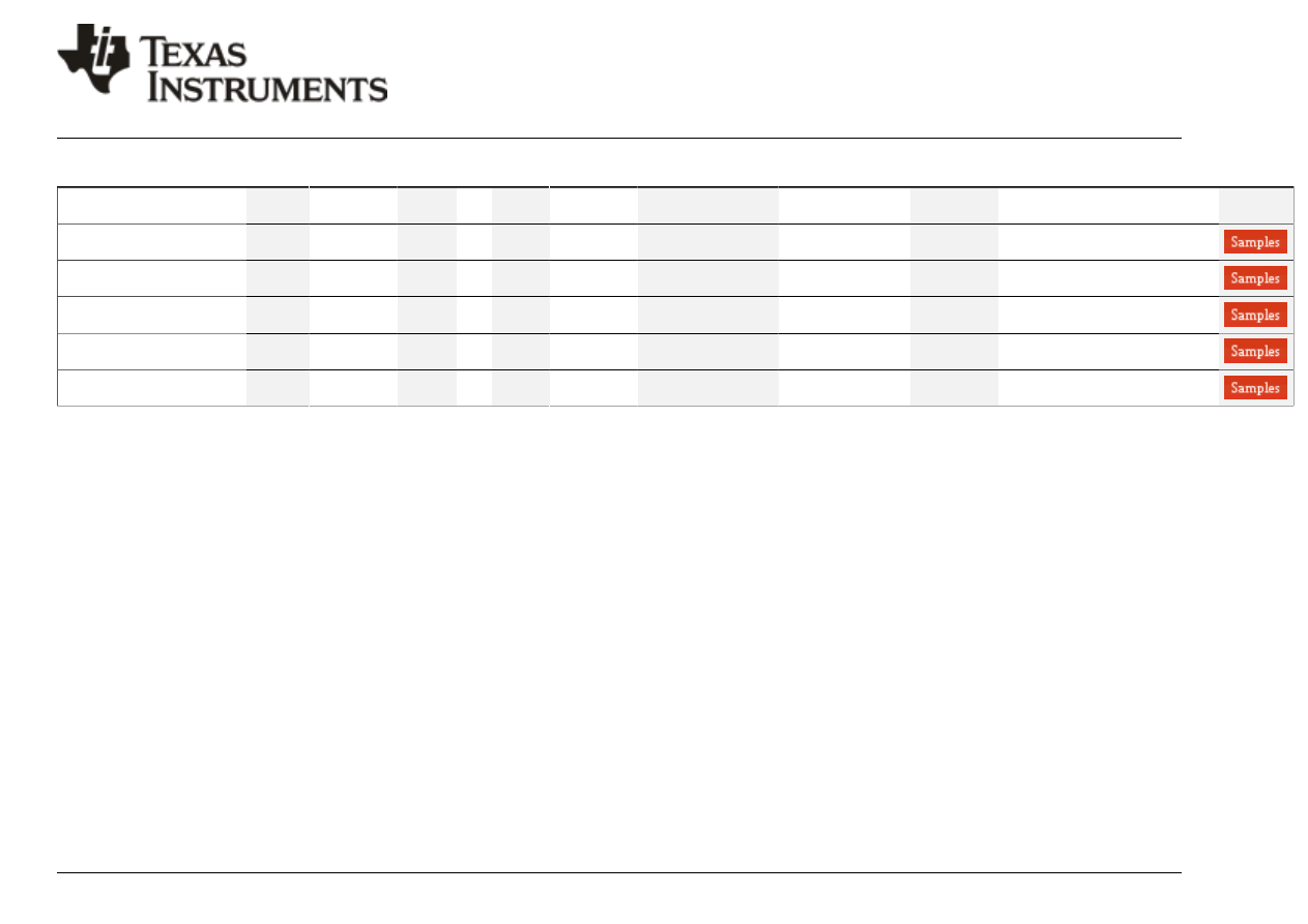
PACKAGING INFORMATION
Orderable Device
Status
(1)
Package Type Package
Drawing
Pins Package
Qty
Eco Plan
(2)
Lead/Ball Finish
(6)
MSL Peak Temp
(3)
Op Temp ( °C)
Device Marking
(4/5)
Samples
LM833D
ACTIVE
SOIC
D
8
75
Green (RoHS
& no Sb/Br)
CU NIPDAU
Level-1-260C-UNLIM
-40 to 85
LM833
LM833DGKR
ACTIVE
VSSOP
DGK
8
2500
Green (RoHS
& no Sb/Br)
CU NIPDAU
Level-1-260C-UNLIM
-40 to 85
RSU
LM833DGKT
ACTIVE
VSSOP
DGK
8
250
Green (RoHS
& no Sb/Br)
CU NIPDAU
Level-1-260C-UNLIM
-40 to 85
RSU
LM833DR
ACTIVE
SOIC
D
8
2500
Green (RoHS
& no Sb/Br)
CU NIPDAU
Level-1-260C-UNLIM
-40 to 85
LM833
LM833P
ACTIVE
PDIP
P
8
50
Pb-Free
(RoHS)
CU NIPDAU
N / A for Pkg Type
-40 to 85
LM833P
(1)
The marketing status values are defined as follows:
ACTIVE: Product device recommended for new designs.
LIFEBUY: TI has announced that the device will be discontinued, and a lifetime-buy period is in effect.
NRND: Not recommended for new designs. Device is in production to support existing customers, but TI does not recommend using this part in a new design.
PREVIEW: Device has been announced but is not in production. Samples may or may not be available.
OBSOLETE: TI has discontinued the production of the device.
(2)
Eco Plan - The planned eco-friendly classification: Pb-Free (RoHS), Pb-Free (RoHS Exempt), or Green (RoHS & no Sb/Br) - please check
for the latest availability
information and additional product content details.
TBD: The Pb-Free/Green conversion plan has not been defined.
Pb-Free (RoHS): TI's terms "Lead-Free" or "Pb-Free" mean semiconductor products that are compatible with the current RoHS requirements for all 6 substances, including the requirement that
lead not exceed 0.1% by weight in homogeneous materials. Where designed to be soldered at high temperatures, TI Pb-Free products are suitable for use in specified lead-free processes.
Pb-Free (RoHS Exempt): This component has a RoHS exemption for either 1) lead-based flip-chip solder bumps used between the die and package, or 2) lead-based die adhesive used between
the die and leadframe. The component is otherwise considered Pb-Free (RoHS compatible) as defined above.
Green (RoHS & no Sb/Br): TI defines "Green" to mean Pb-Free (RoHS compatible), and free of Bromine (Br) and Antimony (Sb) based flame retardants (Br or Sb do not exceed 0.1% by weight
in homogeneous material)
(3)
MSL, Peak Temp. - The Moisture Sensitivity Level rating according to the JEDEC industry standard classifications, and peak solder temperature.
(4)
There may be additional marking, which relates to the logo, the lot trace code information, or the environmental category on the device.
(5)
Multiple Device Markings will be inside parentheses. Only one Device Marking contained in parentheses and separated by a "~" will appear on a device. If a line is indented then it is a continuation
of the previous line and the two combined represent the entire Device Marking for that device.
PACKAGE OPTION ADDENDUM
www.ti.com
21-Jan-2014
Addendum-Page 2
(6)
Lead/Ball Finish - Orderable Devices may have multiple material finish options. Finish options are separated by a vertical ruled line. Lead/Ball Finish values may wrap to two lines if the finish
value exceeds the maximum column width.
Important Information and Disclaimer:The information provided on this page represents TI's knowledge and belief as of the date that it is provided. TI bases its knowledge and belief on information
provided by third parties, and makes no representation or warranty as to the accuracy of such information. Efforts are underway to better integrate information from third parties. TI has taken and
continues to take reasonable steps to provide representative and accurate information but may not have conducted destructive testing or chemical analysis on incoming materials and chemicals.
TI and TI suppliers consider certain information to be proprietary, and thus CAS numbers and other limited information may not be available for release.
In no event shall TI's liability arising out of such information exceed the total purchase price of the TI part(s) at issue in this document sold by TI to Customer on an annual basis.
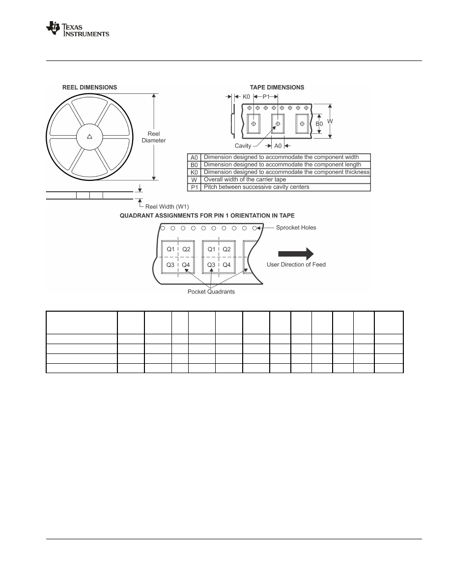
TAPE AND REEL INFORMATION
*All dimensions are nominal
Device
Package
Type
Package
Drawing
Pins
SPQ
Reel
Diameter
(mm)
Reel
Width
W1 (mm)
A0
(mm)
B0
(mm)
K0
(mm)
P1
(mm)
W
(mm)
Pin1
Quadrant
LM833DGKR
VSSOP
DGK
8
2500
330.0
12.4
5.3
3.3
1.3
8.0
12.0
Q1
LM833DGKT
VSSOP
DGK
8
250
180.0
12.4
5.3
3.3
1.3
8.0
12.0
Q1
LM833DR
SOIC
D
8
2500
330.0
12.4
6.4
5.2
2.1
8.0
12.0
Q1
LM833DR
SOIC
D
8
2500
330.0
12.4
6.4
5.2
2.1
8.0
12.0
Q1
PACKAGE MATERIALS INFORMATION
www.ti.com
21-Jan-2014
Pack Materials-Page 1
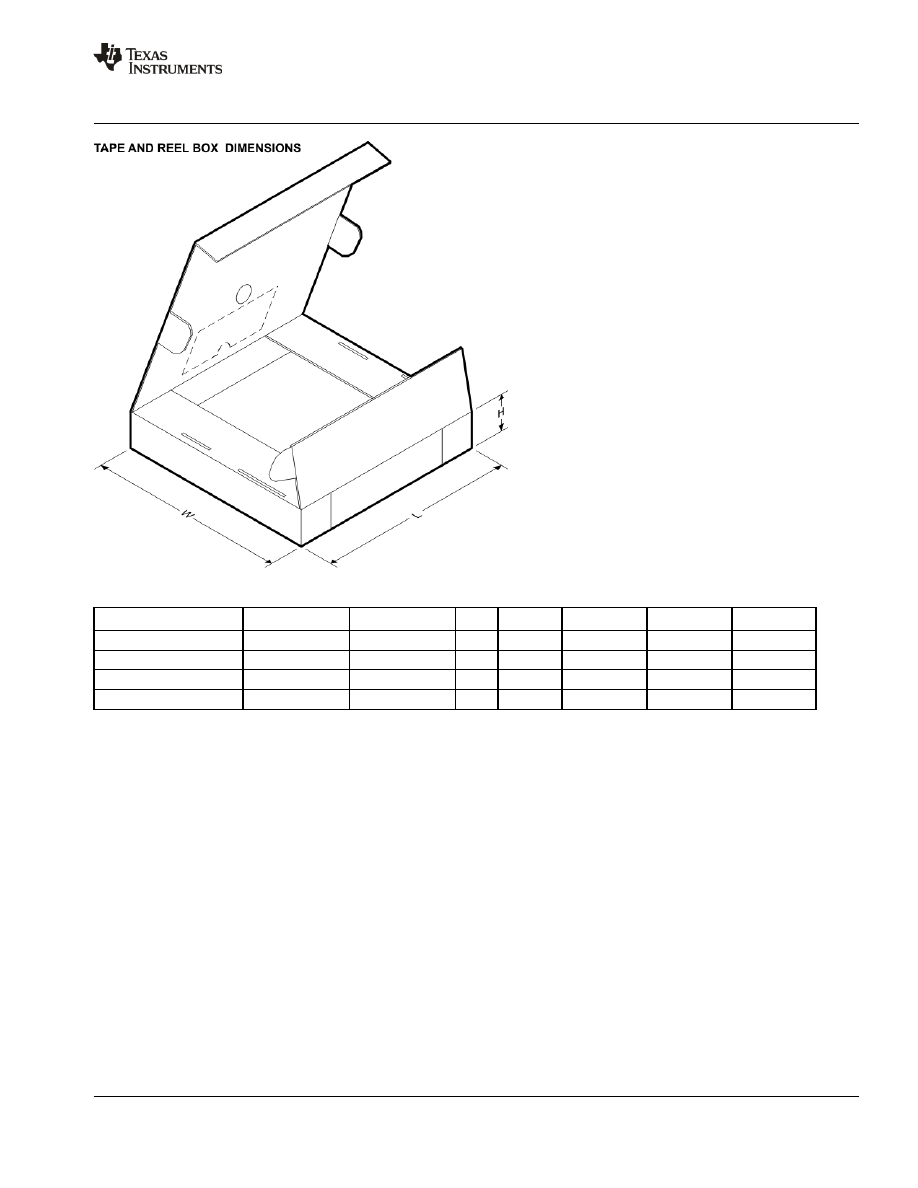
*All dimensions are nominal
Device
Package Type
Package Drawing
Pins
SPQ
Length (mm)
Width (mm)
Height (mm)
LM833DGKR
VSSOP
DGK
8
2500
346.0
346.0
35.0
LM833DGKT
VSSOP
DGK
8
250
203.0
203.0
35.0
LM833DR
SOIC
D
8
2500
367.0
367.0
35.0
LM833DR
SOIC
D
8
2500
340.5
338.1
20.6
PACKAGE MATERIALS INFORMATION
www.ti.com
21-Jan-2014
Pack Materials-Page 2

IMPORTANT NOTICE
Texas Instruments Incorporated and its subsidiaries (TI) reserve the right to make corrections, enhancements, improvements and other
changes to its semiconductor products and services per JESD46, latest issue, and to discontinue any product or service per JESD48, latest
issue. Buyers should obtain the latest relevant information before placing orders and should verify that such information is current and
complete. All semiconductor products (also referred to herein as components) are sold subject to TIs terms and conditions of sale
supplied at the time of order acknowledgment.
TI warrants performance of its components to the specifications applicable at the time of sale, in accordance with the warranty in TIs terms
and conditions of sale of semiconductor products. Testing and other quality control techniques are used to the extent TI deems necessary
to support this warranty. Except where mandated by applicable law, testing of all parameters of each component is not necessarily
performed.
TI assumes no liability for applications assistance or the design of Buyers products. Buyers are responsible for their products and
applications using TI components. To minimize the risks associated with Buyers products and applications, Buyers should provide
adequate design and operating safeguards.
TI does not warrant or represent that any license, either express or implied, is granted under any patent right, copyright, mask work right, or
other intellectual property right relating to any combination, machine, or process in which TI components or services are used. Information
published by TI regarding third-party products or services does not constitute a license to use such products or services or a warranty or
endorsement thereof. Use of such information may require a license from a third party under the patents or other intellectual property of the
third party, or a license from TI under the patents or other intellectual property of TI.
Reproduction of significant portions of TI information in TI data books or data sheets is permissible only if reproduction is without alteration
and is accompanied by all associated warranties, conditions, limitations, and notices. TI is not responsible or liable for such altered
documentation. Information of third parties may be subject to additional restrictions.
Resale of TI components or services with statements different from or beyond the parameters stated by TI for that component or service
voids all express and any implied warranties for the associated TI component or service and is an unfair and deceptive business practice.
TI is not responsible or liable for any such statements.
Buyer acknowledges and agrees that it is solely responsible for compliance with all legal, regulatory and safety-related requirements
concerning its products, and any use of TI components in its applications, notwithstanding any applications-related information or support
that may be provided by TI. Buyer represents and agrees that it has all the necessary expertise to create and implement safeguards which
anticipate dangerous consequences of failures, monitor failures and their consequences, lessen the likelihood of failures that might cause
harm and take appropriate remedial actions. Buyer will fully indemnify TI and its representatives against any damages arising out of the use
of any TI components in safety-critical applications.
In some cases, TI components may be promoted specifically to facilitate safety-related applications. With such components, TIs goal is to
help enable customers to design and create their own end-product solutions that meet applicable functional safety standards and
requirements. Nonetheless, such components are subject to these terms.
No TI components are authorized for use in FDA Class III (or similar life-critical medical equipment) unless authorized officers of the parties
have executed a special agreement specifically governing such use.
Only those TI components which TI has specifically designated as military grade or enhanced plastic are designed and intended for use in
military/aerospace applications or environments. Buyer acknowledges and agrees that any military or aerospace use of TI components
which have not been so designated is solely at the Buyer's risk, and that Buyer is solely responsible for compliance with all legal and
regulatory requirements in connection with such use.
TI has specifically designated certain components as meeting ISO/TS16949 requirements, mainly for automotive use. In any case of use of
non-designated products, TI will not be responsible for any failure to meet ISO/TS16949.
Products
Applications
Audio
Automotive and Transportation
Amplifiers
Communications and Telecom
Data Converters
Computers and Peripherals
DLP ® Products
Consumer Electronics
DSP
Energy and Lighting
Clocks and Timers
Industrial
Interface
Medical
Logic
Security
Power Mgmt
Space, Avionics and Defense
Microcontrollers
Video and Imaging
RFID
OMAP Applications Processors
TI E2E Community
Wireless Connectivity
Mailing Address: Texas Instruments, Post Office Box 655303, Dallas, Texas 75265
Copyright © 2014, Texas Instruments Incorporated
Document Outline

