| Secciones |
|---|
| Foros Electrónica |
|
|
| Boletines de correo |
 |

General Description
The MAX77950 is an advanced wireless power receiver
IC that meets the specification requirements for WPC
low-power (v1.2) and PMA SR1 (v2.0) communication
protocols. This device operates using near-field magnetic
induction when coupled with a WPC or PMA transmitter
and provides output power up to 12 watts.
The IC has precision output current and voltage-sensing
scheme over the entire load range. It enables accurate
received power packets, as defined in the WPC specifications
for best foreign object detection (FOD). The IC supports
FSK demodulation to receive PMA advertisement ID as
well as WPC FSK packets.
The IC features the patent-pending PeerPower
™ function.
In PeerPower mode, the IC operates as a transmitter,
enabling power transfer to another peer device through
in-band ASK communications.
The MAX77950 communicates with an application pro-
cessor through an I ²C serial interface. The status of power
transfer and alerts are read through this interface.
Applications
Smartphones
Tablets
Smart Watches
Headsets
Wearable Devices
Battery-Power Banks
Wi-Fi Hotspots
Digital Cameras
Portable Medical Applications
Portable Media Players
Point-of-Sale Devices
Handheld Devices
PeerPower is a trademark of Maxim Integrated Products, Inc.
19-100003; Rev 0; 3/17
Benefits and Features
WPC/PMA Dual Mode Wireless Power Receiver
Compliant with WPC Low Power (v1.2) and PMA
SR1 (v2.0)
Peer-to-Peer Power Transmission with In-Band ASK
Communications
WPC ASK Demodulator/FSK Demodulator
Output Programmable Range from 3.5V to 12.7V
with 100mV Step
Integrated High-Efficiency n-Channel Full-Bridge
Synchronous Rectifier
Programmable Foreign Object Detection
Programmable Dynamic Rectifier-Voltage Scaling
Overvoltage, Overcurrent, and Overtemperature
Protection
MAX77950
WPC/PMA Dual Mode Wireless Power Receiver
EVALUATION KIT AVAILABLE

TABLE OF CONTENTS
www.maximintegrated.com
Maxim Integrated
2
MAX77950
WPC/PMA Dual Mode Wireless Power Receiver

TABLE OF CONTENTS (CONTINUED)
www.maximintegrated.com
Maxim Integrated
3
MAX77950
WPC/PMA Dual Mode Wireless Power Receiver

TABLE OF CONTENTS (CONTINUED)
www.maximintegrated.com
Maxim Integrated
4
MAX77950
WPC/PMA Dual Mode Wireless Power Receiver

LIST OF FIGURES
TABLE OF CONTENTS (CONTINUED)
www.maximintegrated.com
Maxim Integrated
5
MAX77950
WPC/PMA Dual Mode Wireless Power Receiver
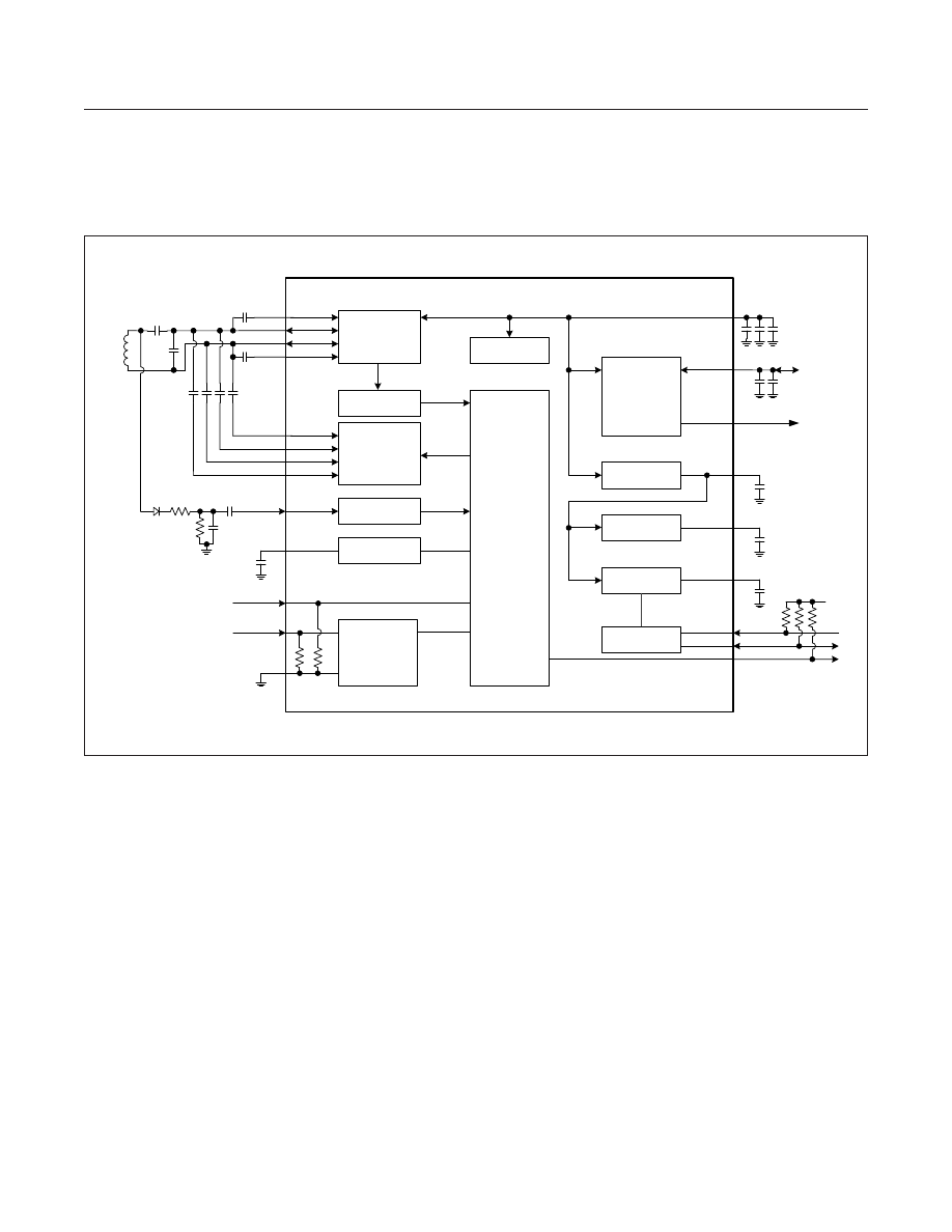
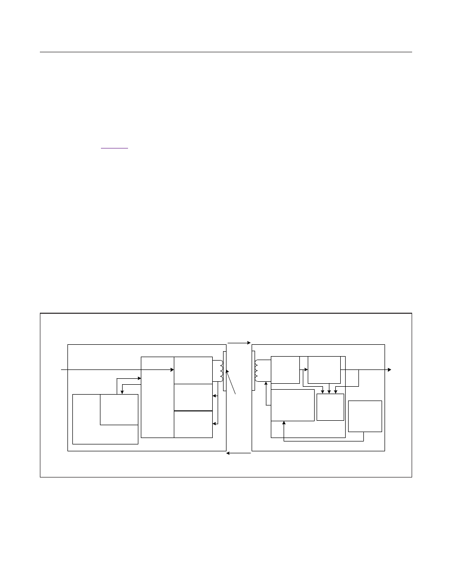
Simplified Block Diagram
LDO/
PeerPower
SWITCH/
WP DETECTION
V
RECT
FSM
SYNC-
RECTIFIER/
INVERTER
FSK
DEMODULATION
DMODIN
BPF FILTER/ASK
DEMODULATOR
12 BIT ADC
ADCREF
1 µF
SCL
I
2
C SLAVE
SDA
WP_DET
LDO V
DD
1 µF
1 µF
LDO V
CC
V
CC
AC2
Ls
AC1
10 µF x 3
10 µF x 2
PRECLAMP /
DC LOAD
1 µF
V
OUT
V
DD
LDO 1.8V
V1P8
SYS_I/O
BOOT1
BOOT2
COMM1
CLAMP2
CLAMP1
COMM2
47
nF
ASK
MODULATOR/
OV CLAMP
Cs
Cd
SBIAS/ REF
DIS
INT
800
k٦
47
nF
47
nF
47
nF
15nF
15nF
800
k٦
P2PEN
AGND
MAX77950
www.maximintegrated.com
Maxim Integrated
6
MAX77950
WPC/PMA Dual Mode Wireless Power Receiver

AC1, AC2 to PGND ...............................................-0.3V to +20V
V
RECT
, V
OUT
to PGND .........................................-0.3V to +20V
COMM1, COMM2, CLAMP1, CLAMP2 to PGND .-0.3V to +20V
BST1, BST2 to PGND ...........................................-0.3V to +25V
Differential ABS-MAX: BST1 to AC1, BST2 to AC2 ..........+4.5V
V
CC
to AGND .......................................................-0.3V to +4.5V
V
DD
to AGND .....................................................-0.3V to +1.65V
V1P8 to AGND .....................................................-0.3V to +4.5V
SCL, SDA, INT to AGND ......................................-0.3V to +4.5V
DIS to AGND .............................................-0.3V to V1P8 + 0.3V
WP_DET to AGND ....................................-0.3V to V1P8 + 0.3V
P2PEN to AGND .......................................-0.3V to V1P8 + 0.3V
DMODIN to AGND .......................................-0.3V to V
CC
+ 0.3V
ADCREF to AGND ......................................-0.3V to V
DD
+ 0.3V
DNC .............................................................-0.3V to V
CC
+ 0.3V
AGND to PGND ....................................................-0.3V to +0.3V
AC1, AC2 Current.................................................................2.5A
V
OUT
Current ....................................................... -1.5A to +1.5A
COMM1, COMM2 ....................................................................1A
CLAMP1, CLAMP2 ...............................................................1.5A
Operating Ambient Temperature Range ............. -40 °C to +85 °C
Junction Temperature ....................................... -40 °C to +150 °C
Soldering Temperature (reflow) .......................................+260 °C
Absolute Maximum Ratings
Stresses beyond those listed under Absolute Maximum Ratings may cause permanent damage to the device. These are stress ratings only, and functional operation of the device at these
or any other conditions beyond those indicated in the operational sections of the specifications is not implied. Exposure to absolute maximum rating conditions for extended periods may affect
device reliability.
Package Code
W546A9+1 (6x9, 0.4mm pitch)
Outline Number
Land Pattern Number
THERMAL RESISTANCE, FOUR-LAYER BOARD:
Junction to Ambient (Θ
JA
)
40 °C/W
Junction to Case (Θ
JC
)
N/A
Package thermal resistances were obtained using the method described in JEDEC specification JESD51-7, using a four-layer board.
For detailed information on package thermal considerations,
.
For the latest package outline information and land patterns (footprints), go to
. Note that a +,
#, or - in the package code indicates RoHS status only. Package drawings may show a different suffix character, but the drawing
pertains to the package regardless of RoHS status.
Package Information
www.maximintegrated.com
Maxim Integrated
7
MAX77950
WPC/PMA Dual Mode Wireless Power Receiver

(V
RECT
= 3V to 20V, T
A
= -40 °C to +85 °C, unless otherwise noted, limits are 100% tested at T
A
= +25 °C; limits over the operating
temperature range and relevant supply voltage range are guaranteed by design and characterization, unless otherwise noted.)
PARAMETER
SYMBOL
CONDITIONS
MIN
TYP
MAX
UNITS
Input Supply Current
I
VRECT
No load
5
mA
Disable Supply Current
I
VRECT_SHDN
DIS = 1, V
RECT
= 5V
2.1
mA
Disable supply Current
I
VRECT_SHDN
DIS = 1, V
RECT
= 20V
2.2
mA
Undervoltage Lockout
Threshold
V
UVLO
V
RECT
rising
2.4
2.9
V
Undervoltage Lockout
Hysteresis
V
UVLO_HYS
400
mV
Internal Pulldown Resistance
for DIS and P2PEN
R
PD
Pulldown resistance to AGND
400
800
1600
kΩ
VOLTAGE REGULATORS
Voltage Regulator for
Internal Blocks
V
CC
4.06
4.275
4.49
V
V
DD
1.496
1.575
1.65
V1P8 Voltage Regulator
V1P8
I
V1P8
= 20mA
1.71
1.8
1.89
V
LDO
HV LDO Input Voltage
Range
V
RECT
3
20
V
V
OUT
Programmable
Range Through I
2
C
V
OUTPRG
100mV step
3.5
12.7
V
HV LDO Startup Rate
t
LDOSTUP
I
OUT
= 0mA
0.5
V/ms
HV LDO Line Regulation
∆V
OUT
/∆V
IN
LDO_VOUTSET[6:0] = 0x32, I
OUT
= 1mA;
V
RECT
= 6V to 12V
0.1
%
HV LDO Load Regulation
∆V
OUT
/∆I
OUT
LDO_VOUTSET[6:0] = 0x32, I
OUT
= 1mA to
1A, V
RECT
= 5.2V
0.5
%
HV LDO Load Transient
I
OUT
= 1mA to 1A and 1A to 1mA within 20 µs
±8
%
HV LDO Dropout Voltage
V
DO
LDO_VOUTSET[6:0] = 0x32, I
OUT
= 1A,
V
DO
= V
RECT
-V
OUT
100
mV
HV LDO Current Limit
I
LIM
LDO_ILIMSET[4:0] = 0x1A, LDO_VOUT-
SET[6:0] = 0x32, V
RECT
= +5.1V, V
OUT
=
+4.8V
1.1
1.5
A
Output Voltage Initial
Accuracy
V
OUT_ACC
LDO_VOUTSET[6:0] = 0x32, I
OUT
= 1mA,
T
A
= +25 °C
-2
+2
%
COMM PINS
COMMn On-Resistance
R
COMM
1
Ω
COMMn Leakage Current
I
COMM
V
COMM1
= V
COMM2
= 20V, T
A
= +25 °C
1
μA
CLAMP PINS
CLAMPn On-Resistance
R
CLAMP
0.5
Ω
CLAMPn Leakage Current
I
CLAMP
V
CLAMP1
= V
CLAMP2
= 20V, T
A
= +25 °C
1
μA
OVP Preclamp Threshold
OVLO
PRECLAMP
V
RECT
rising
16
V
Electrical Characteristics
www.maximintegrated.com
Maxim Integrated
8
MAX77950
WPC/PMA Dual Mode Wireless Power Receiver

(V
RECT
= 3V to 20V, T
A
= -40 °C to +85 °C, unless otherwise noted, limits are 100% tested at T
A
= +25 °C; limits over the operating
temperature range and relevant supply voltage range are guaranteed by design and characterization, unless otherwise noted.)
PARAMETER
SYMBOL
CONDITIONS
MIN
TYP
MAX
UNITS
SYNCHRONOUS RECTIFIER
High-Side Switch
On-Resistance
R
ON_HS
50
mΩ
Low-Side Switch
On-Resistance
R
ON_LS
50
mΩ
ADC
ADC Reference Voltage
V
ADC_REF
No load
1.237
1.25
1.262
V
Initial ADC Accumulated
Error for V
RECT
ADC_ERR_VRECT V
RECT
= 3V to 15V, production tested at
3.5V, 7.5V, and 14.5V
-1
+1
%
Initial ADC Accumulated
Error for V
OUT
ADC_ERR_VOUT V
OUT
= 3.6V to 10V, production tested at
3.5V, 6.5V, and 9.5V
-1
+1
%
Initial ADC Accumulated
Error for ISNS
ADC_ERR_ISNS Current range 0 to 1A, T
A
= +25 °C
-10
+10
mA
DEMODULATOR
DMODIN Input Resistance
0.7
mΩ
DMODIN Minimum
Detectable Input Voltage
200
mV
THERMAL PROTECTION
Thermal Shutdown
T
JOFF
T
J
rising
165
°C
Thermal-Shutdown
Hysteresis
T
JOFFHYS
T
J
falling
10
°C
Temperature-Warning
Threshold
T
JWARN
120
°C
LOGIC OUTPUT
WP_DET Output High
Voltage
Source current 5mA
V1P8 -
0.4
V
WP_DET Output
Low Voltage
Sink current 5mA
0.4
V
INTB Output Low Voltage
V
OL
Sink current 20mA
0.4
V
LOGIC INPUT
P2PEN Input High Voltage
1.4
V
P2PEN Input Low Voltage
0.4
V
P2PEN Input Leakage
Current
1
μA
DIS Input High Voltage
1.4
V
DIS Input Low Voltage
0.4
V
DIS Input Leakage Current
1
μA
Electrical Characteristics (continued)
www.maximintegrated.com
Maxim Integrated
9
MAX77950
WPC/PMA Dual Mode Wireless Power Receiver

Note 1: Limits are 100% production tested at T
A
= +25 °C. Limits over the operating temperature range and relevant supply voltage
range are guaranteed by design and characterization.
Note 2: All voltages are referenced to AGND.
Note 3: Test is performed on unmounted/unsoldered ports.
Note 4: f
SCL
must meet the minimum clock low time plus the rise/fall times.
Note 5: The maximum t
HD:DAT
has to be met only if the device does not stretch the low period (t
LOW
) of the SCL signal.
(V
RECT
= 3V to 20V, T
A
= -40 °C to +85 °C, unless otherwise noted, limits are 100% tested at T
A
= +25 °C; limits over the operating
temperature range and relevant supply voltage range are guaranteed by design and characterization, unless otherwise noted.)
PARAMETER
SYMBOL
CONDITIONS
MIN
TYP
MAX
UNITS
I
2
C INTERFACE
SCL, SDA Input
High Voltage
V
IH
1.4
V
SCL, SDA Input
Low Voltage
V
IL
0.4
V
SCL, SDA Input Hysteresis
V
HYS
0.2
V
SCL, SDA Input Leakage
Current
I
I
0.1 x V
DD
< SCL/SDA < 0.9 x V
DD
-1
+1
μA
SDA Output Low Voltage
V
OL
Sinking 10mA
0.4
V
SCL, SDA Pin Capacitance
C
I
10
pF
Output Fall Time from
V
IH
to V
IL
t
OF
300
ns
Clock Frequency
f
SCL
0
400
kHz
Hold Time Repeated
Start Condition
t
HD;STA
Note 4
0.6
μs
SCL Low Period
t
LOW
1.3
μs
SCL High Period
t
HIGH
0.6
μs
Setup Time Repeated
Start Condition
t
SU_STA
0.6
μs
Data Hold Time
t
HD_DAT
Note 5
0
0.9
μs
Data Setup Time
t
SU_DAT
100
ns
Setup Time for STOP
Condition
t
SU_STO
0.6
μs
Bus Free Time Between
STOP and START Condition
t
BUF
1.3
μs
Data Valid Time
t
VD:DAT
0.9
μs
Data Valid Acknowledge
Time
t
VD:ACK
0.9
μs
Bus Capacitance
C
B
550
pF
Pulse Width of Suppressed
Spikes
t
SP
Maximum pulse width of spikes that must be
suppressed by the input filter
50
ns
Electrical Characteristics (continued)
www.maximintegrated.com
Maxim Integrated
10
MAX77950
WPC/PMA Dual Mode Wireless Power Receiver
(Using WPC A11 and PMA 7 transmitters at T
A
= +25 °C, unless otherwise noted.)
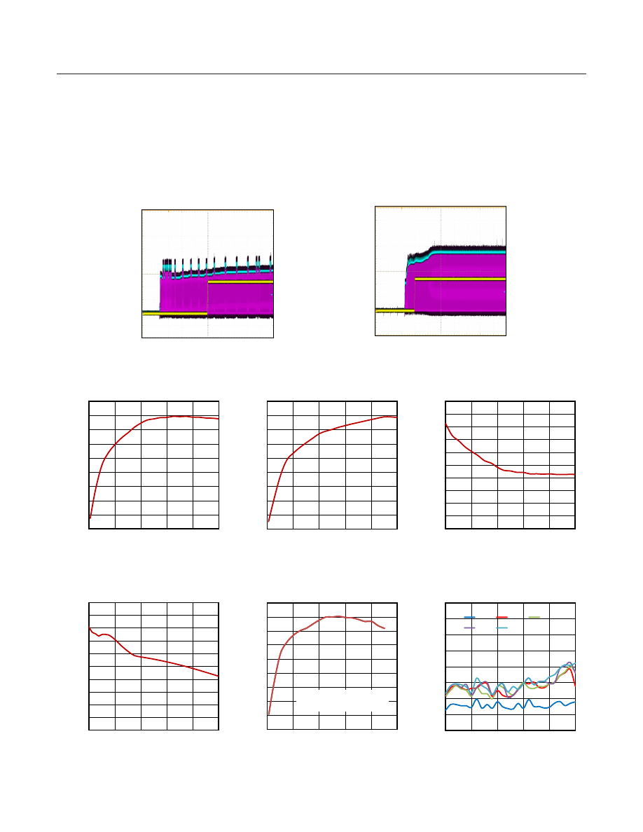
Typical Operating Characteristics
2V/div
toc01
200ms/div
V
OUT
V
RECT
AC1
WPC MODE NO LOAD START-UP
2V/div
2V/div
2V/div
toc01
200ms/div
V
OUT
V
RECT
AC1
2V/div
2V/div
0
10
20
30
40
50
60
70
80
90
0
200
400
600
800
1000
EF
FI
CI
EN
CY
(%
)
LOAD CURRENT (mA)
PMA MODE DC-DC EFFICIENCY
toc04
0
10
20
30
40
50
60
70
80
90
0
200
400
600
800
1000
EF
FI
CI
EN
CY
(%
)
LOAD CURRENT (mA)
PeerPower MODE DC-DC EFFICIENCY
toc07
COIL PART NUMBER
Tx: SUNLORD SWA30N30H20C01B
Rx: SUNLORD SWA30R30H08C01B
2V/div
toc02
200ms/div
V
OUT
V
RECT
AC1
PMA MODE NO LOAD START-UP
2V/div
2V/div
3.0
3.5
4.0
4.5
5.0
5.5
6.0
6.5
7.0
7.5
8.0
0
200
400
600
800
1000
V
R
EC
T
(V
)
LOAD CURRENT (mA)
RECTIFIER VOLTAGE IN WPC MODE
toc05
-400
-350
-300
-250
-200
-150
-100
-50
0
0
200
400
600
800
1000
PP
T-
PP
R
(m
W
)
LOAD CURRENT (mA)
Center
Up
Down
Left
Right
WPC FOREIGN OBJECT DETECTION
toc08
0
10
20
30
40
50
60
70
80
90
0
200
400
600
800
1000
EF
FI
CI
EN
CY
(%
)
LOAD CURRENT (mA)
WPC MODE DC-DC EFFICIENCY
toc03
3.0
3.5
4.0
4.5
5.0
5.5
6.0
6.5
7.0
7.5
8.0
0
200
400
600
800
1000
V
R
EC
T
(V
)
LOAD CURRENT (mA)
RECTIFIER VOLTAGE IN PMA MODE
toc06
Maxim Integrated
11
www.maximintegrated.com
MAX77950
WPC/PMA Dual Mode Wireless Power Receiver
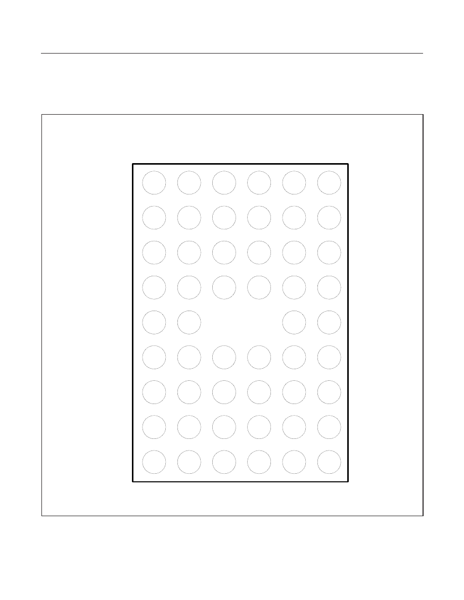
Bump Configuration
PGND
PGND
PGND
PGND
PGND
PGND
AC1
AC1
DNC
DNC
AC2
AC2
BST1
AC1
DNC
DMODIN
AC2
BST2
V
CC
V
RECT
V
RECT
V
RECT
V
RECT
V1P8
V
RECT
V
RECT
V
RECT
V
RECT
V
OUT
V
OUT
V
OUT
V
OUT
V
OUT
V
OUT
PGND
N.C.
INT
WP_DET
V
DD
PGND
CLAMP1
P2PEN
SDA
AGND
DIS
CLAMP2
COMM1
DNC
SCL
ADCREF
DNC
COMM2
A
B
C
D
E
F
G
H
J
1
2
3
4
5
6
TOP VIEW
(BUMP SIDE DOWN)
( 52-Bump WLP, 0.4mm pitch )
TOP VIEW
(BUMP SIDE DOWN)
www.maximintegrated.com
Maxim Integrated
12
MAX77950
WPC/PMA Dual Mode Wireless Power Receiver

PIN
NAME
FUNCTION
TYPE
A1
COMM1
Open-Drain Output. Achieves the AC modulation to communicate with the Tx.
Digital Output
A2, A5, G3,
H3, H4
DNC
Do Not Connect. Leave open in system.
Analog I/O
A3
SCL
I
2
C Clock Input
Digital Input
A4
ADCREF
ADC Reference Voltage. Bypass to ground with a 1μF ceramic capacitor.
Analog Output
A6
COMM2
Open-Drain Output. Achieves the AC modulation to communicate with the Tx.
Digital Output
B1
CLAMP1
Open-Drain Outputs. Switches to modulate ASK to communicate with Tx. Turns on
when V
RECT
overvoltage event occurs.
Digital Output
B2
P2PEN
PeerPower function active-high enable input.
Digital Input
B3
SDA
I
2
C Data Input/Output
Digital I/O
B4
AGND
Analog Reference Ground. "Star-ground" connection to system GND.
Ground
B5
DIS
Disable Pin, Active-High
Digital Input
B6
CLAMP2
Open-Drain Outputs. Switches to modulate ASK to communicate with Tx. Turns on
when V
RECT
overvoltage event occurs.
Digital Output
C1, C6, J1- J6
PGND
Power Ground
Ground
C2
N.C.
Not Internally Connected. Can connect to power, ground, or leave open.
No Connect
C3
INT
Open-Drain, Active-Low Interrupt Output
Digital Output
C4
WP_DET
Wireless Power Detected Output. Active-high
Digital Output
C5
V
DD
+1.575V linear regulator low ripple output for internal use. Bypass to ground with a
1μF ceramic capacitor.
Power Output
D1-D6
V
OUT
Linear Regulator Output. Bypass to ground with two 10μF capacitors.
Power I/O
E1, E2, F2-F5,
E5, E6
V
RECT
Rectifier's Output. Bypass to ground with three 10μF and one 100nF ceramic
capacitor.
Power I/O
F1
V
CC
+4.275V linear regulator low ripple output for internal use. Bypass to ground with a
1μF ceramic capacitor.
Power Output
F6
V1P8
+1.8V linear regulator low ripple output. Bypass to ground with a 1μF ceramic
capacitor.
Power Output
G1
BST1
Bootstrap pin for rectifier's high side n-channel FET gate driver.
Analog Output
G2, H1, H2
AC1
Rectifier Input. Connect to receiver LC tank.
Power Input
G4
DMODIN
Amplitude Shift Keying Demodulator Input
Analog Input
G5, H5, H6
AC2
Rectifier Input. Connect to receiver LC tank.
Power Input
G6
BST2
Bootstrap pin for rectifier's high side n-channel FET gate driver
Analog Output
Bump Description
www.maximintegrated.com
Maxim Integrated
13
MAX77950
WPC/PMA Dual Mode Wireless Power Receiver
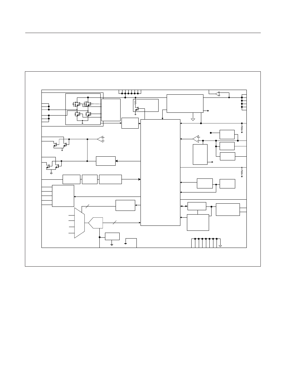
1.25V
ADC REF
OSC
(4MHz)
PLL
(16x)
LDO V
CC
(4.275V)
LDO V
DD
(1.575V)
ASK
MODULATOR
OVP
V
OUT
ISNS
TDIE
2
AC2
ADCREF
V
CC
V
DD
VCC
UVTH
VOK
PGND
PGND
PGND
PGND
SYNC-RECTIFIER / INVERTER
P2PEN
AC1
AC1
AC2
I
2
C SLAVE
REGISTER
BANK
SCL
SDA
INT
64MHz
BOOT1
BOOT2
CLAMP1
CLAMP2
COMM
COMM1
COMM2
AGND
RECTIFIER/
INVERTER
CONTROLLER
OTP
Q1
Q2
Q3
Q4
Q5
Q6
Q7
Q8
V
RECT
LOWPASS
FILTER
AFE ASK
DEMODULATOR
V
RECT
ADC
MUX
12-BIT
ADC
HIGHPASS
FILTER
FSK
DEMOD
FSM
12
ADC
SEQUENCER
DMODIN
PGND
PGND
PGND
PGND
BIAS, BG/
SBIAS
AC2
AC1
LDO
(1.8V)
V1P8
4MHz
TEST
CONTROLLER
DNC
DNC
DNC
DNC
N.C.
MAIN FSM FOR WPC/PMA Rx
FUNCTIONALITY
TDIE
VREF
WP
_DET
V
RECT
V
RECT
DC-LOAD/
PRECLAMP
HV-LDO /
PeerPower SWITCH
V
RECT
ISNS
ILIM
V
OUT
V
OUT
DNC
DIS
V
RECT
V
RECT
V
RECT
V
RECT
V
RECT
V
RECT
V
RECT
V
OUT
V
OUT
V
OUT
V
OUT
V
OUT
MAX77950
Functional Diagram
www.maximintegrated.com
Maxim Integrated
14
MAX77950
WPC/PMA Dual Mode Wireless Power Receiver
Detailed Description
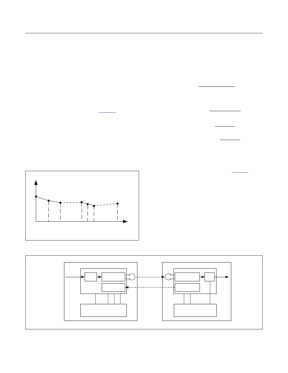
Wireless Power Transfer System Overview
A wireless power system consists of a base station on
the primary side and a power receiver on the secondary
side, as shown
. The base station (referred
to as a power transmitter), comprises a power conver-
sion unit, primary coil, communications demodulator, and
control unit. The power receiver comprises a secondary
coil, power pick-up unit, communications modulator, and
controller.
When the receiver is placed on top of the transmitters
interface surface, the magnetic field that is generated
by the primary coil induces a voltage on the secondary
coil when the coils are magnetically coupled together.
The output voltage of the receiver is regulated, and the
received power is controlled through the communications
and control unit in the receiver. The receiver communi-
cates with the transmitter for requesting increased power,
decreased power, no change in power transfer, or power-
transfer termination. This communication is conducted in-
band between the coils and is digitally overlaid on top of
the power signal. The impedance on the secondary side
is modulated as the receiver communicates, which is cap-
tured as load modulation by the primary coil. The trans-
mitter changes frequency, duty cycle, or even voltage
input of the power inverter to meet the demand of power
that the receiver requests through the communication.
In WPC mode, the transmitter detects the modulation of
the current and/or voltage across the primary coil and
demodulates communication messages known as pack-
ets. A few examples of WPC packets are control error
packet, received power packet, and end power transfer
packet. The digital communication scheme, in the WPC
protocol, utilizes differential bi-phase encoding as ONE
and ZERO bits are transferred from the secondary to pri-
mary at a rate of 2kbps.
The PMA communication protocol operates continuously
to transmit symbol messages that are encoded through
frequency-based modulation. The receiver can send six
different types of symbols to the transmitter using different
frequency rates between 250Hz and 8kHz. They include
decrement (DEC), increment (INC), no change (NoCh),
end of charge (EOC), MsgBit, and a proprietary symbol
intended for future use.
Figure 1. Wireless Power Transfer System Diagram
COMMUNICATIONS
AND CONTROL UNIT
BASE STATION
VOLTAGE/
CURRENT
SENSE
POWER
INVERTER
POWER RECEIVER
POWER PICK-UP UNIT
VOLTAGE/
CURRENT
SENSE
RECTIFIER
VOLTAGE/
CURRENT
REGULATOR
COMMUNICATION
MODULATOR
POWER
CONTROL
ALGORITHMS
/ WPC, PMA
PROTOCOLS
POWER
CONTROL
ALGORITHMS
AND WPC, PMA
PROTOCOLS
DC OUTPUT
DC INPUT
PRIMARY
COIL
SECONDARY
COIL
INTERFACE
SURFACE
POWER
TRANSFER
COMMUNICATION
DEMODULATOR
POWER
CONVERSION
UNIT
www.maximintegrated.com
Maxim Integrated
15
MAX77950
WPC/PMA Dual Mode Wireless Power Receiver
Rectified-Voltage Control Loop
The rectified voltage (V
RECT
) is regulated by a closed
control loop between the wireless power transmitter (base
station) and the wireless power receiver (mobile device).
To achieve the best compromise between optimal effi-
ciency and output load transient response, the rectified
voltage is regulated based on the output current. The
V
RECT
profile versus the load can be programmed in the
following
The V
RECT
target voltage is stored in eight 8-bit reg-
isters allocated for WPC mode (VRECT_TARGET_Y0
to VRECT_TARGET_Y7) and eight 8-bit registers allo-
cated for PMA mode (VRECT_TARGET_PMA_Y0 to
VRECT_TARGET_PMA_Y7). The output current is divid-
ed into eight thresholds which are stored in the registers
VRECT_TARGET_X0 to VRECT_TARGET_X7. Different
V
RECT
target profiles are used for WPC and PMA due to
the different power transfer profile characteristics.
The following equation calculates the V
RECT
target based
on linear interpolation between the adjacent coefficients:
y = yn-1 +
(
x - xn-1
)(
yn-yn-1
)
xn-xn-1
Where X is the actual output current reading:
VRECT_TARGET_Xn =
Xn
(
A
)
× 255 × 0.73
1.25
VRECT_TARGET_Yn =
Yn
(
V
)
× 255
1.25 × 12
VRECT_TARGET_PMA_Yn =
Yn
(
V
)
× 255
1.25 × 12
PeerPower Function
Overview
The PeerPower function enables one mobile device to
charge another mobile device wirelessly.
shows
the main concept.
The MAX77950 is a highly configurable wireless power IC
that allows the user to reconfigure the rectifier into a full-
bridge inverter, achieving high-efficiency power transfer
due to low R
DS(ON)
of the power MOSFETs.
Once P2PEN is pulled high, the switch located between
V
OUT
and V
RECT
is turned on and the inverter generates
a digital ping repeatedly. The IC continues power transfer
once it receives the signal strength packet and also termi-
nates power transfer after the end power transfer packet
is received. A demodulated packet is stored in the regis-
ters (such as TX_WPC_HEADER, TX_WPC_DATA0/../7)
until the next packet comes.
Figure 2. Rectified Voltage Profile vs. Output Current
Figure 3. System-Level Block Diagram in PeerPower Mode
(X
0,
Y0
)
I
OUT
(X
1,
Y1
)
(X
2,
Y2
)
(Xn
-1
, Yn
-1
)
(X
7,
Y7
)
[A]
X
Y
(Xn
, Yn
)
Xn-1
Xn
X
Y
X7
X0
X1
X2
SWITCH
INVERTER
RECTIFIER
LDO
Tx-COIL
Rx-COIL
5V TO 10V
INPUT
V
OUT
SCL
SDA
P2
PEN
(HIGH
)
SCL
SDA
P2
PEN
(LOW
)
MOBILE DEVICE IN Tx MODE
POWER
ASK
MODULATOR
ASK
DEMODULATOR
COMMUNICATION
(ASK)
APPLICATION PROCESSOR
OR HOST µC
MOBILE DEVICE IN Rx MODE
APPLICATION PROCESSOR
OR HOST µC
INT
www.maximintegrated.com
Maxim Integrated
16
MAX77950
WPC/PMA Dual Mode Wireless Power Receiver
In PeerPower mode, the IC can generate interrupts in
power transfer phase whenever it receives WPC packets
that are non-zero CEP, RPP, CSP, EPT, and PPP so that
an application processor or microcontroller notices it. To
make this, a user needs to enable the ASK_DEMOD_PT_
INT_EN bit. Then, INT goes low and the ASK_DEMOD_
PT bit is set whenever the IC receives packets in power
transfer phase.
To operate the IC in PeerPower mode, the following steps
must be followed:
1) Supply an input voltage to the output of the LDO
(V
OUT
pin).
2) Program initial frequency into TX_FOP_SET_H/L;
otherwise, the inverter will operate at 125kHz since it
is the default frequency.
3) Pull P2PEN pin high to make LDO be a switch and
run the inverter.
Wireless Power Detection Function
The IC offers a WP_DET output that is a power-good indi-
cator that monitors the V
OUT
level. The WP_DET output
goes high once V
OUT
exceeds the level programmed in
WPDET_H_Threshold[1:0] and it goes low once V
OUT
drops down to the level programmed in WPDET_L_
Threshold[1:0].
Clamp Function
An overvoltage event may occur when the mobile device
is moved over the transmitters surface, or when partially
removed from the mobile device and quickly placed on
the power transmitter. In addition, it may occur during
the ping stage in PMA mode. The IC has preclamp and
clamp features to limit the rectifier-output voltage as an
overvoltage protection. The preclamp pulls 250mA from
V
RECT
to PGND when the voltage on V
RECT
exceeds
16V. If the rectifier-output voltage reaches 17V, even after
the preclamp is activated, the IC turns on FETs between
CLAMP1/2 and PGND as an additional protection. The
preclamp and the clamp thresholds are both program-
mable through I
2
C.
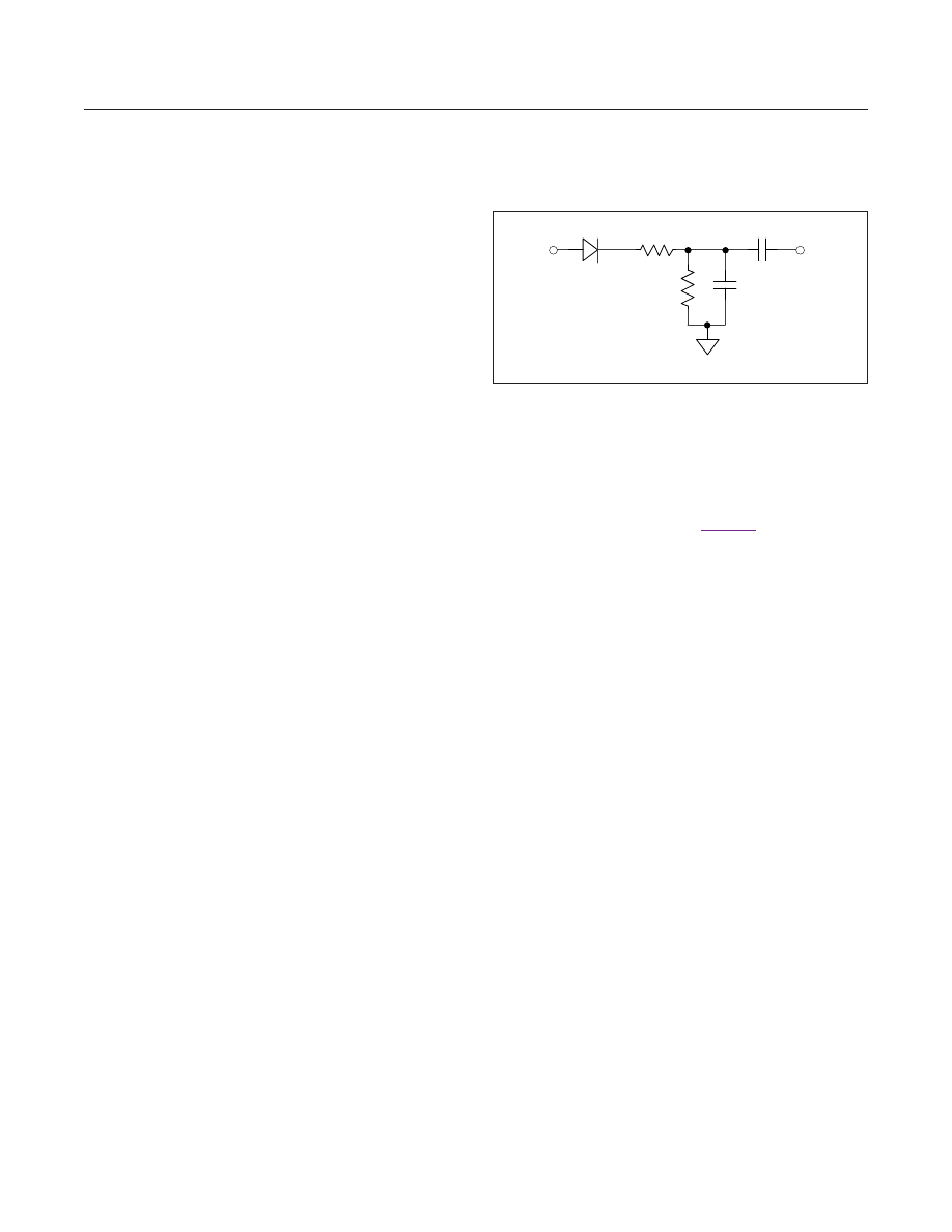
ASK/FSK Demodulation
The IC contains an ASK demodulation block that demodu-
lates WPC ASK in PeerPower mode. In WPC, transmitted
power is coupled to the receiver coil. When the receiver is
powered up, it communicates with the transmitter at 2kHz
by modulating the impedance of the receiver coil with
communication capacitors. The function of the IC's ASK
demodulator is to detect the 2kHz communication signal
from the power signal.
The external circuits, shown in
are required for
the ASK demodulation in PeerPower mode. If the user
application does not require PeerPower mode, the circuit
is not necessary, so connect the DMODIN pin to GND.
The IC can demodulate the PMA advertising packet and
WPC FSK with the FSK demodulation block.
The IC demodulates WPC FSK by using positive (+)
polarity with modulation depth 0 following WPC Power
Class 0 specification, version 1.2.1.
Foreign Object Detection (FOD)
As stated in the WPC specifications, a foreign object is
defined as any object positioned on the interface surface
of a base station but not part of the mobile device, such
as coins, keys, or other metals. If the foreign object is
within the active area, it may heat up during the power
transfer, due to eddy currents, resulting from the oscil-
lating magnetic field. Power loss is the key to detecting
foreign objects and limiting the power loss on a wireless
power system actually limits the heat. To start a power-
transfer cycle during the selection phase, the transmit-
ter detects and locates objects that are placed on the
interface surface and attempts to differentiate between
the foreign objects and a possible power receiver device.
Once the wireless power receiver is discovered and the
power transmitter completes the identification and the
configuration phase, the power receiver reports to the
power transmitter its received power in a received power
packet (P
RECEIVED
).
Figure 4. External Circuits for Envelope Detection, Level
Shifting, and AC Coupling
AC1
(FROM COIL)
DMODIN
www.maximintegrated.com
Maxim Integrated
17
MAX77950
WPC/PMA Dual Mode Wireless Power Receiver
The received power (P
PR
) equals the power available
from the output of the power receiver, plus any power lost
in producing that output power. For example, the power
loss includes, but is not limited to:
Power loss in the secondary coil and series resonant
capacitor
Power loss in the shielding of the power receiver
Power loss in the rectifier
Power loss in any post-regulation stage
Eddy current loss in metal components or contacts
within the power receiver
The IC complies with the WPC low-power (v1.2) requirement:
P
RECEIVED
- 350mW ≤ P
PR
≤ P
RECEIVED
This means that the reported received power is an over-
estimate of the actual received power, by 350mW, where
P
PR
is the actual received power determined by the
mobile device by measuring its load power and adding the
estimated parasitic power losses.
The IC has high-precision output current-sensing capa-
bilities and accurate V
RECT
control over the operating
load, ensuring they are sufficient to estimate the received
power and comply with WPC (v1.2) FOD requirements.
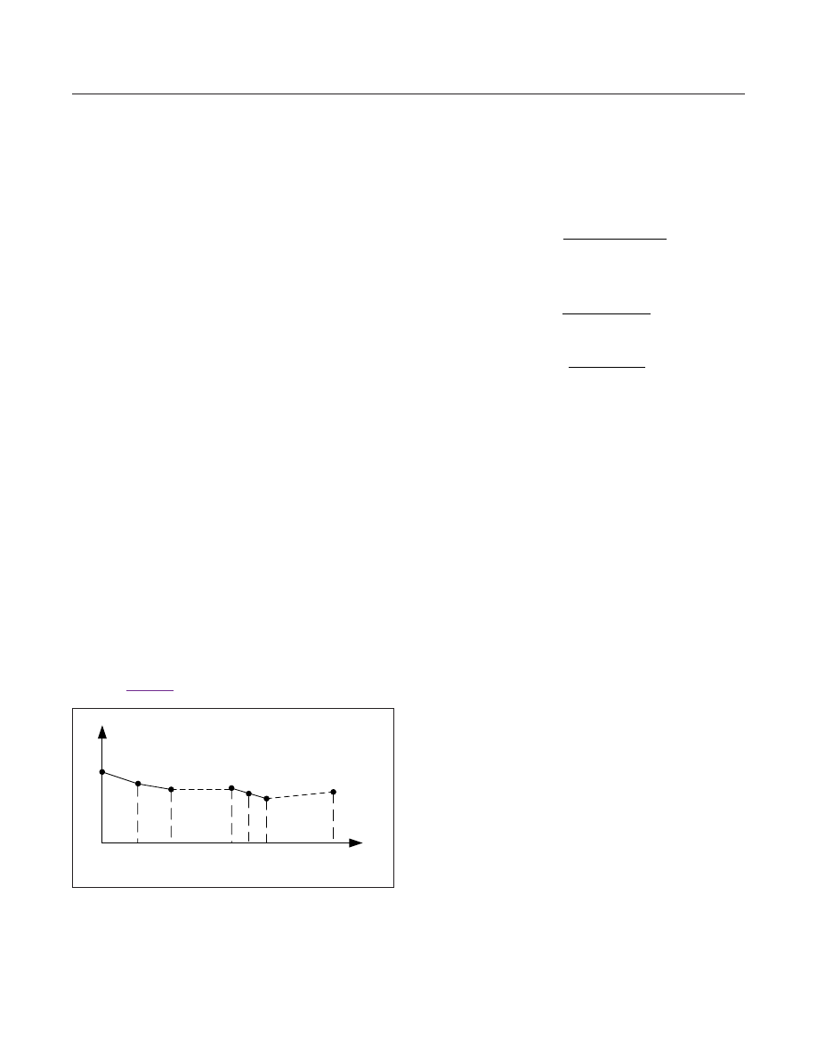
The IC provides registers that are FOD_Xn and FOD_Yn
as part of the received power look-up table (LUT). Based
on this LUT, the state machine sends a received power
packet that is specified in the WPC requirements.
FOD_Xn stores 16 X-coordinates for output current val-
ues and FOD_Yn stores 16 Y-coordinates of received
power values so it makes 16 pairs of coordinates, as
shown in
Between each coordinate, the values are interpolated
linearly, as shown in the following equation:
y = yn-1 +
(
x - xn-1
)(
yn-yn-1
)
xn-xn-1
Equations for the FOD register are:
FOD_Xn =
Xn
(
A
)
× 255 × 0.73
1.25
FOD_Yn =
Yn
(
W
)
× 128 × 2
10
Watchdog Function
The IC supports a watchdog function that disables the main
LDO output in case the watchdog timer expires. When the
WDOG_INT_EN bit is set, it enables the watchdog function
as well as the associated interrupt (WDOG_INT). The
default timer is 41.5s. To keep the main LDO outputs
after setting the WDOG_INT_EN bit, an application
processor must periodically set the WDOG_INT_CLR bit
before the timer expires. If the WDOG_INT_CLR bit is
set, the timer is reset, and the WDOG_INT bit cleared.
This feature prevents the IC from supplying power to a
charger when the application processor freezes. To turn
the main LDO back on, the application processor needs to
set the WDOG_INT_CLR and Toggle_LDO bits. The timer
options are programmable by OTP.
Sending End Power Transfer (EPT)/End of
Charge (EOC)
The WPC EPT packet and the PMA EOC symbol is sent
to a transmitter only by setting SEND_EPT bit 1 in RX_
COM register (address : 0x20) or pulling the DIS pin high.
The IC state machine does not send EPT or EOC by itself.
Sending Proprietary Packets (PPP)
The IC supports PPP, that is defined in the WPC
specifications. The maximum length of a PPP is 5 bytes
of messages. An example procedure for sending a PPP
(3 bytes of messages) is as follows:
1. Write 0x38 in PPP_HEADER[7:0]
2. Write the first message in RX_DATA_VALUE0[7:0]
3. Write the second message in RX_DATA_VALUE1[7:0]
4. Write the third message in RX_DATA_VALUE2[7:0]
5. Set SEND_RX_DATA bit in RX_COM[7:0]
Figure 5. FOD Coefficients vs. Load Current
(X
0,
Y0
)
I
OUT
(X
1,
Y1
)
(X
2,
Y2
)
(Xn
-1
, Yn
-1
)
(X
15
, Y
15
)
[A]
X
Y
(Xn
, Yn
)
Xn-1
Xn
X
Y
X15
X0
X1
X2
www.maximintegrated.com
Maxim Integrated
18
MAX77950
WPC/PMA Dual Mode Wireless Power Receiver

Register Map
ADDRESS
NAME
MSB
LSB
FUNCTIONAL
0x00
CHIP_ID[7:0]
CHIP_ID[7:0]
0x05
OTP_REV[7:0]
OTP_REV[7:0]
0x06
STATUS_L[7:0]
STAT_
VOUT
STAT_
VRECT
STAT_
WDOG FSK_RCVDRESERVEDRESERVED
OVER_
VOLTAGE
OVER_
CURRENT
0x07
STATUS_H[7:0]
OVER_
TEMP
TX_OVER_
CURRENT
TX_OVER_
TEMP
RESERVED TX_CONN ASK_DE-
MOD_PING
ASK_DE-
MOD_IDCF
ASK_DE-
MOD_PT
0x08
INT_L[7:0]
VOUT_INT VRECT_
INT
WDOG_INT
FSK_
RCVD_INT RESERVEDRESERVED OV_INT
OC_INT
0x09
INT_H[7:0]
OT_INT
TX_OC_
INT
TX_OT_INTRESERVEDTX_CONN_
INT
ASK_DE-
MOD_
PING_INT
ASK_DE-
MOD_
IDCF_INT
ASK_DE-
MOD_PT_
INT
0x0A
INT_ENABLE_L[7:0]
VOUT_
INT_EN
VRECT_
INT_EN
WDOG_
INT_EN
FSK_
RCVD_
INT_EN
RESERVEDRESERVED OV_INT_
EN
OC_INT_
EN
0x0B
INT_ENABLE_H[7:0] OT_INT_
EN
TX_OC_
INT_EN
TX_OT_
INT_EN RESERVED
TX_CONN_
INT_EN
ASK_DE-
MOD_
PING_INT_
EN
ASK_DE-
MOD_
IDCF_INT_
EN
ASK_DE-
MOD_PT_
INT_EN
0x0C
INT_CLEAR_L[7:0]
VOUT_
INT_CLR
VRECT_
INT_CLR
WDOG_
INT_CLR
FSK_
RCVD_
INT_CLR
RESERVEDRESERVED OV_INT_
CLR
OC_INT_
CLR
0x0D
INT_CLEAR_H[7:0]
OT_INT_
CLR
TX_OC_
INT_CLR
TX_OT_
INT_CLR RESERVED
TX_CONN_
INT_CLR
ASK_DE-
MOD_
PING_INT_
CLR
ASK_DE-
MOD_
IDCF_INT_
CLR
ASK_DE-
MOD_PT_
INT_CLR
0x0E
CHARGE_STA-
TUS[7:0]
CHARGE_STATUS[7:0]
0x0F
EPT_REASON[7:0]
EPT_REASON[7:0]
0x10
VOUTVAL_H[7:0]
VOUTVAL[11:4]
0x11
VOUTVAL_L[7:0]
RESERVED[3:0]
VOUTVAL[3:0]
0x12
VOUTSET[7:0]
RE-
SERVED
VOUTSET[6:0]
0x13
VRECT_ADJ[7:0]
VRECT_ADJ[7:0]
0x14
VRECTVAL_H[7:0]
VRECTVAL[11:4]
0x15
VRECTVAL_L[7:0]
RESERVED[3:0]
VRECTVAL[3:0]
0x16
ISENSEVAL_H[7:0]
ISENSEVAL[11:4]
0x17
ISENSEVAL_L[7:0]
RESERVED[3:0]
ISENSEVAL[3:0]
0x18
TDIE_VALUE[7:0]
TDIE_VALUE[7:0]
0x19
OP_FREQ_L[7:0]
OP_FREQ[7:0]
0x1A
OP_FREQ_H[7:0]
OP_FREQ[15:8]
0x1B
PING_OP_
FREQ_L[7:0]
PING_OP_FREQ[7:0]
www.maximintegrated.com
Maxim Integrated
19
MAX77950
WPC/PMA Dual Mode Wireless Power Receiver

Register Map (continued)
ADDRESS
NAME
MSB
LSB
0x1C
PING_OP_
FREQ_H[7:0]
PING_OP_FREQ[15:8]
0x1D
LDO_ILIMSET[7:0]
RESERVED[2:0]
LDO_ILIMSET[4:0]
0x1E
TX_ILIMSET[7:0]
RESERVED[2:0]
TX_ILIMSET[4:0]
0x1F
SYS_OP_MODE[7:0]
SYS_OP_MODE[7:0]
0x20
RX_COM[7:0]
RE-
SERVED
RE-
SERVED
CLEAR_IN-
TERRUPT
SEND_
CHARGE_
STATUS
SEND_EPT
RE-
SERVED
TOGGLE_
LDO
SEND_RX_
DATA
0x21
PPP_HEADER[7:0]
PPP_HEADER[7:0]
0x22
RX_DATA_VAL-
UE0[7:0]
RX_DATA_VALUE0[7:0]
0x23
RX_DATA_VAL-
UE1[7:0]
RX_DATA_VALUE1[7:0]
0x24
RX_DATA_VAL-
UE2[7:0]
RX_DATA_VALUE2[7:0]
0x25
RX_DATA_VAL-
UE3[7:0]
RX_DATA_VALUE3[7:0]
0x26
RX_DATA_VAL-
UE4[7:0]
RX_DATA_VALUE4[7:0]
0x27
FSK_DATA_VAL-
UE0[7:0]
FSK_DATA_VALUE0[7:0]
0x28
FSK_DATA_VAL-
UE1[7:0]
FSK_DATA_VALUE1[7:0]
0x29
FSK_DATA_VAL-
UE2[7:0]
FSK_DATA_VALUE2[7:0]
0x2A
TX_FOP_SET_L[7:0]
TX_FOP_SET[7:0]
0x2B
TX_FOP_SET_H[7:0]
RESERVED[6:0]
TX_FOP_
SET[8]
0x2C
TX_FOP_TON_
SET_L[7:0]
TX_FOP_TON_SET[7:0]
0x2D
TX_FOP_TON_
SET_H[7:0]
RESERVED[6:0]
TX_FOP_
TON_
SET[8]
0x34
TX_WPC_HEAD-
ER[7:0]
TX_WPC_HEADER[7:0]
0x35
TX_WPC_DATA0[7:0]
TX_WPC_DATA0[7:0]
0x36
TX_WPC_DATA1[7:0]
TX_WPC_DATA1[7:0]
0x37
TX_WPC_DATA2[7:0]
TX_WPC_DATA2[7:0]
0x38
TX_WPC_DATA3[7:0]
TX_WPC_DATA3[7:0]
0x39
TX_WPC_DATA4[7:0]
TX_WPC_DATA4[7:0]
0x3A
TX_WPC_DATA5[7:0]
TX_WPC_DATA5[7:0]
0x3B
TX_WPC_DATA6[7:0]
TX_WPC_DATA6[7:0]
www.maximintegrated.com
Maxim Integrated
20
MAX77950
WPC/PMA Dual Mode Wireless Power Receiver

Register Map (continued)
ADDRESS
NAME
MSB
LSB
0x3C
TX_WPC_DATA7[7:0]
TX_WPC_DATA7[7:0]
0x3D
TX_WPC_CHECK-
SUM[7:0]
TX_WPC_CHECKSUM[7:0]
0x3E
FOD_X0[7:0]
FOD_X0[7:0]
0x3F
FOD_Y0[7:0]
FOD_Y0[7:0]
0x40
FOD_X1[7:0]
FOD_X1[7:0]
0x41
FOD_Y1[7:0]
FOD_Y1[7:0]
0x42
FOD_X2[7:0]
FOD_X2[7:0]
0x43
FOD_Y2[7:0]
FOD_Y2[7:0]
0x44
FOD_X3[7:0]
FOD_X3[7:0]
0x45
FOD_Y3[7:0]
FOD_Y3[7:0]
0x46
FOD_X4[7:0]
FOD_X4[7:0]
0x47
FOD_Y4[7:0]
FOD_Y4[7:0]
0x48
FOD_X5[7:0]
FOD_X5[7:0]
0x49
FOD_Y5[7:0]
FOD_Y5[7:0]
0x4A
FOD_X6[7:0]
FOD_X6[7:0]
0x4B
FOD_Y6[7:0]
FOD_Y6[7:0]
0x4C
FOD_X7[7:0]
FOD_X7[7:0]
0x4D
FOD_Y7[7:0]
FOD_Y7[7:0]
0x4E
FOD_X8[7:0]
FOD_X8[7:0]
0x4F
FOD_Y8[7:0]
FOD_Y8[7:0]
0x50
FOD_X9[7:0]
FOD_X9[7:0]
0x51
FOD_Y9[7:0]
FOD_Y9[7:0]
0x52
FOD_X10[7:0]
FOD_X10[7:0]
0x53
FOD_Y10[7:0]
FOD_Y10[7:0]
0x54
FOD_X11[7:0]
FOD_X11[7:0]
0x55
FOD_Y11[7:0]
FOD_Y11[7:0]
0x56
FOD_X12[7:0]
FOD_X12[7:0]
0x57
FOD_Y12[7:0]
FOD_Y12[7:0]
0x58
FOD_X13[7:0]
FOD_X13[7:0]
0x59
FOD_Y13[7:0]
FOD_Y13[7:0]
0x5A
FOD_X14[7:0]
FOD_X14[7:0]
0x5B
FOD_Y14[7:0]
FOD_Y14[7:0]
0x5C
FOD_X15[7:0]
FOD_X15[7:0]
0x5D
FOD_Y15[7:0]
FOD_Y15[7:0]
0x62
OV_CLAMP_VOLT-
AGE[7:0]
RESERVED[2:0]
POV_
CLAMP_
VOLTAGE
RESERVED[1:0]
OV_CLAMP_VOLT-
AGE[1:0]
0x63
TX_LAST_CEP[7:0]
TX_LAST_CEP[7:0]
www.maximintegrated.com
Maxim Integrated
21
MAX77950
WPC/PMA Dual Mode Wireless Power Receiver

Register Map (continued)
ADDRESS
NAME
MSB
LSB
0x64
TX_LAST_RPP[7:0]
TX_LAST_RPP[7:0]
0x65
TX_LAST_PCHP[7:0]
TX_LAST_PCHP[7:0]
LDO
0x70
LDO_WPDET_
CNFG[7:0]
WPDET_H_DE-
BOUNCE[1:0]
WPDET_L_DE-
BOUNCE[1:0]
WPDET_H_THRESH-
OLD[1:0]
WPDET_L_THRESH-
OLD[1:0]
VRECT_TARGET
0xBA
VRECT_TARGET_
X0[7:0]
VRECT_TARGET_X0[7:0]
0xBB
VRECT_TARGET_
Y0[7:0]
VRECT_TARGET_Y0[7:0]
0xBC
VRECT_TARGET_
PMA_Y0[7:0]
VRECT_TARGET_PMA_Y0[7:0]
0xBD
VRECT_TARGET_
X1[7:0]
VRECT_TARGET_X1[7:0]
0xBE
VRECT_TARGET_
Y1[7:0]
VRECT_TARGET_Y1[7:0]
0xBF
VRECT_TARGET_
PMA_Y1[7:0]
VRECT_TARGET_PMA_Y1[7:0]
0xC0
VRECT_TARGET_
X2[7:0]
VRECT_TARGET_X2[7:0]
0xC1
VRECT_TARGET_
Y2[7:0]
VRECT_TARGET_Y2[7:0]
0xC2
VRECT_TARGET_
PMA_Y2[7:0]
VRECT_TARGET_PMA_Y2[7:0]
0xC3
VRECT_TARGET_
X3[7:0]
VRECT_TARGET_X3[7:0]
0xC4
VRECT_TARGET_
Y3[7:0]
VRECT_TARGET_Y3[7:0]
0xC5
VRECT_TARGET_
PMA_Y3[7:0]
VRECT_TARGET_PMA_Y3[7:0]
0xC6
VRECT_TARGET_
X4[7:0]
VRECT_TARGET_X4[7:0]
0xC7
VRECT_TARGET_
Y4[7:0]
VRECT_TARGET_Y4[7:0]
0xC8
VRECT_TARGET_
PMA_Y4[7:0]
VRECT_TARGET_PMA_Y4[7:0]
0xC9
VRECT_TARGET_
X5[7:0]
VRECT_TARGET_X5[7:0]
0xCA
VRECT_TARGET_
Y5[7:0]
VRECT_TARGET_Y5[7:0]
0xCB
VRECT_TARGET_
PMA_Y5[7:0]
VRECT_TARGET_PMA_Y5[7:0]
www.maximintegrated.com
Maxim Integrated
22
MAX77950
WPC/PMA Dual Mode Wireless Power Receiver

Register Map (continued)
ADDRESS
NAME
MSB
LSB
0xCC
VRECT_TARGET_
X6[7:0]
VRECT_TARGET_X6[7:0]
0xCD
VRECT_TARGET_
Y6[7:0]
VRECT_TARGET_Y6[7:0]
0xCE
VRECT_TARGET_
PMA_Y6[7:0]
VRECT_TARGET_PMA_Y6[7:0]
0xCF
VRECT_TARGET_
X7[7:0]
VRECT_TARGET_X7[7:0]
0xD0
VRECT_TARGET_
Y7[7:0]
VRECT_TARGET_Y7[7:0]
0xD1
VRECT_TARGET_
PMA_Y7[7:0]
VRECT_TARGET_PMA_Y7[7:0]
DEMOD
0xDB
PMA_ADV_DATA[7:0]
PMA_ADV_DATA[7:0]
0xDC
PMA_ADV_CRC[7:0]
RESERVED[3:0]
PMA_ADV_CRC[3:0]
CHIP_ID (0x00)
BIT
7
6
5
4
3
2
1
0
Field
CHIP_ID[7:0]
Reset
0b0001_0010
Access Type
Read Only
BITFIELD
BITS
DESCRIPTION
CHIP_ID
7:0
-
OTP_REV (0x05)
BIT
7
6
5
4
3
2
1
0
Field
OTP_REV[7:0]
Reset
0b0000_0000
Access Type
Read Only
BITFIELD
BITS
DESCRIPTION
OTP_REV
7:0
OTP revision
www.maximintegrated.com
Maxim Integrated
23
MAX77950
WPC/PMA Dual Mode Wireless Power Receiver

STATUS_L (0x06)
BIT
7
6
5
4
3
2
1
0
Field
STAT_
VOUT
STAT_
VRECT
STAT_
WDOG
FSK_RCVD RESERVED RESERVED
OVER_
VOLTAGE
OVER_
CURRENT
Reset
0b0
0b0
0b0
0b0
0b0
0b0
0b0
0b0
Access Type
Read Only
Read Only
Read Only
Read Only
Read Only
Read Only
Read Only
Read Only
BITFIELD
BITS
DESCRIPTION
STAT_VOUT
7
1: LDO is ON
0: LDO is OFF (Rx ONLY)
STAT_VRECT
6
1: V
RECT
is over UVLO (Rx ONLY)
STAT_WDOG
5
1: Watchdog timer expires
0: No watchdog timer expires
FSK_RCVD
4
1: FSK data sent by transmitter is received
0: No FSK data
RESERVED
3
RSVD
RESERVED
2
RSVD
OVER_VOLTAGE
1
1: Overvoltage (V
RECT
)
0: Normal
OVER_CURRENT
0
1: Overcurrent (LDO output current) in Rx mode
0: Normal
STATUS_H (0x07)
BIT
7
6
5
4
3
2
1
0
Field
OVER_
TEMP
TX_OVER_
CURRENT
TX_OVER_
TEMP
RESERVED
TX_CONN
ASK_DE-
MOD_PING
ASK_DE-
MOD_IDCF
ASK_DE-
MOD_PT
Reset
0b0
0b0
0b0
0b0
0b0
0b0
0b0
0b0
Access Type
Read Only
Read Only
Read Only
Read Only
Read Only
Read Only
Read Only
Read Only
BITFIELD
BITS
DESCRIPTION
OVER_TEMP
7
1: Overtemperature in Rx mode
0: Normal
TX_OVER_CURRENT
6
1: Overcurrent in Tx mode
0: Normal
TX_OVER_TEMP
5
1: Overtemperature in Tx mode
0: Normal
RESERVED
4
RSVD
TX_CONN
3
1: Power transfer established in Tx mode
0: No power transfer established
ASK_DEMOD_PING
2
1: Packet received in PING phase
0: No packet
ASK_DEMOD_IDCF
1
1: Packet received in ID and configuration phase
0: No packet
ASK_DEMOD_PT
0
1: Packet received in power transfer phase (count CEP if that is non zero)
0: No packet
www.maximintegrated.com
Maxim Integrated
24
MAX77950
WPC/PMA Dual Mode Wireless Power Receiver

INT_L (0x08)
BIT
7
6
5
4
3
2
1
0
Field
VOUT_INT VRECT_INT WDOG_INT
FSK_
RCVD_INT RESERVED RESERVED
OV_INT
OC_INT
Reset
0b0
0b0
0b0
0b0
0b0
0b0
0b0
0b0
Access Type
Read Only
Read Only
Read Only
Read Only
Read Only
Read Only
Read Only
Read Only
BITFIELD
BITS
DESCRIPTION
VOUT_INT
7
1: V
OUT
state change (off to on, on to off)
VRECT_INT
6
1: V
RECT
is over UVLO (Rx ONLY)
WDOG_INT
5
1: Watchdog timer expired
FSK_RCVD_INT
4
1: FSK data sent by transmitter is received
RESERVED
3
RSVD
RESERVED
2
RSVD
OV_INT
1
1: Overvoltage (V
RECT
)
0: Normal
OC_INT
0
1: Overcurrent (LDO output current) in Rx mode
0: Normal
INT_H (0x09)
BIT
7
6
5
4
3
2
1
0
Field
OT_INT
TX_OC_INT TX_OT_INT RESERVED TX_CONN_
INT
ASK_DE-
MOD_
PING_INT
ASK_DE-
MOD_
IDCF_INT
ASK_DE-
MOD_PT_
INT
Reset
0b0
0b0
0b0
0b0
0b0
0b0
0b0
0b0
Access Type
Read Only
Read Only
Read Only
Read Only
Read Only
Read Only
Read Only
Read Only
BITFIELD
BITS
DESCRIPTION
OT_INT
7
1: Overtemperature in Rx mode
TX_OC_INT
6
1: Overcurrent in Tx mode
TX_OT_INT
5
1: Overtemperature in Tx mode
RESERVED
4
RSVD
TX_CONN_INT
3
1: Power tranfer phase established in Tx mode
ASK_DEMOD_PING_
INT
2
1: Packet received in PING Phase
ASK_DEMOD_IDCF_
INT
1
1: Packet received in ID and configuration phase
ASK_DEMOD_PT_INT
0
1: Packet received in power transfer phase
www.maximintegrated.com
Maxim Integrated
25
MAX77950
WPC/PMA Dual Mode Wireless Power Receiver

INT_ENABLE_L (0x0A)
BIT
7
6
5
4
3
2
1
0
Field
VOUT_INT_
EN
VRECT_INT_
EN
WDOG_INT_
EN
FSK_RCVD_
INT_EN
RESERVED RESERVED OV_INT_EN OC_INT_EN
Reset
0b0
0b0
0b0
0b0
0b0
0b0
0b0
0b0
Access Type Write, Read Write, Read Write, Read Write, Read Write, Read Write, Read Write, Read Write, Read
BITFIELD
BITS
DESCRIPTION
VOUT_INT_EN
7
1: Enable VOUT_INT
0: Disable
VRECT_INT_EN
6
1: Enable VRECT_INT
0: Disable
WDOG_INT_EN
5
1: Enable watchdog timer and associated interrupt
0: Disable
FSK_RCVD_INT_EN
4
1: Enable FSK_RCVD_INT
0: Disable
RESERVED
3
RSVD
RESERVED
2
RSVD
OV_INT_EN
1
1: Enable OV_INT
0: Disable
OC_INT_EN
0
1: Enable OC_INT
0: Disable
INT_ENABLE_H (0x0B)
BIT
7
6
5
4
3
2
1
0
Field
OT_INT_EN TX_OC_INT_
EN
TX_OT_INT_
EN
RESERVED TX_CONN_
INT_EN
ASK_DE-
MOD_PING_
INT_EN
ASK_DE-
MOD_IDCF_
INT_EN
ASK_DE-
MOD_PT_
INT_EN
Reset
0b0
0b0
0b0
0b0
0b0
0b0
0b0
0b0
Access Type Write, Read Write, Read Write, Read Write, Read Write, Read Write, Read Write, Read Write, Read
BITFIELD
BITS
DESCRIPTION
OT_INT_EN
7
1: Enable OT_INT
0: Disable
TX_OC_INT_EN
6
1: Enable TX_OC_INT
0: Disable
TX_OT_INT_EN
5
1: Enable TX_OT_INT
0: Disable
RESERVED
4
RSVD
TX_CONN_INT_EN
3
1: Enable TX_CONN_INT
0: Disable
ASK_DEMOD_PING_
INT_EN
2
1: Enable ASK_DEMOD_PING_INT
0: Disable
ASK_DEMOD_IDCF_
INT_EN
1
1: Enable ASK_DEMOD_IDCF_INT
0: Disable
ASK_DEMOD_PT_INT_
EN
0
1: Enable ASK_DEMOD_PT_INT
0: Disable
www.maximintegrated.com
Maxim Integrated
26
MAX77950
WPC/PMA Dual Mode Wireless Power Receiver

INT_CLEAR_L (0x0C)
BIT
7
6
5
4
3
2
1
0
Field
VOUT_INT_
CLR
VRECT_
INT_CLR
WDOG_
INT_CLR
FSK_
RCVD_INT_
CLR
RESERVED RESERVED
OV_INT_
CLR
OC_INT_
CLR
Reset
0b0
0b0
0b0
0b0
0b0
0b0
0b0
0b0
Access Type Write, Read Write, Read Write, Read Write, Read Write, Read Write, Read Write, Read Write, Read
BITFIELD
BITS
DESCRIPTION
VOUT_INT_CLR
7
1: Clear VOUT_INT bit (this CLR bit resets automatically after being set)
VRECT_INT_CLR
6
1: Clear VRECT_INT bit (this CLR bit resets automatically after being set)
WDOG_INT_CLR
5
1: Clear WDOG_INT bit (this CLR bit resets automatically after being set)
FSK_RCVD_INT_CLR
4
1: Clear FSK_RCVD_INT (this CLR bit resets automatically after being set)
RESERVED
3
RSVD
RESERVED
2
RSVD
OV_INT_CLR
1
1: Clear OV_INT bit (this CLR bit resets automatically after being set)
OC_INT_CLR
0
1: Clear OC_INT bit (this CLR bit resets automatically after being set)
INT_CLEAR_H (0x0D)
BIT
7
6
5
4
3
2
1
0
Field
OT_INT_
CLR
TX_OC_
INT_CLR
TX_OT_
INT_CLR
RESERVED TX_CONN_
INT_CLR
ASK_DE-
MOD_
PING_INT_
CLR
ASK_DE-
MOD_
IDCF_INT_
CLR
ASK_DE-
MOD_PT_
INT_CLR
Reset
0b0
0b0
0b0
0b0
0b0
0b0
0b0
0b0
Access Type Write, Read Write, Read Write, Read Write, Read Write, Read Write, Read Write, Read Write, Read
BITFIELD
BITS
DESCRIPTION
OT_INT_CLR
7
1: Clear OT_INT bit (this CLR bit resets automatically after being set)
TX_OC_INT_CLR
6
1: Clear TX_OC_INT bit (this CLR bit resets automatically after being set)
TX_OT_INT_CLR
5
1: Clear TX_OT_INT bit (this CLR bit resets automatically after being set)
RESERVED
4
RSVD
TX_CONN_INT_CLR
3
1: Clear TX_CONN_INT bit (this CLR bit resets automatically after being set)
ASK_DEMOD_PING_
INT_CLR
2
1: Clear ASK_DEMOD_PING_INT bit (this CLR bit resets automatically after
being set)
ASK_DEMOD_IDCF_
INT_CLR
1
1: Clear ASK_DEMOD_IDCF_INT bit (this CLR bit resets automatically after
being set)
ASK_DEMOD_PT_INT_
CLR
0
1: Clear ASK_DEMOD_PT_INT bit (this CLR bit resets automatically after
being set)
www.maximintegrated.com
Maxim Integrated
27
MAX77950
WPC/PMA Dual Mode Wireless Power Receiver

CHARGE_STATUS (0x0E)
BIT
7
6
5
4
3
2
1
0
Field
CHARGE_STATUS[7:0]
Reset
0b1111_1111
Access Type
Write, Read
BITFIELD
BITS
DESCRIPTION
CHARGE_STATUS
7:0
Register for storing charge status as follows:
0x00: Reserved
0x01: Charge status = 1 (1%)
0x02: Charge status = 2 (2%)
¦..
0x64: Charge status = 64 (100%)
0x65 to 0xFE: Reserved
0xFF: No battery charge device or not providing charge status packet
EPT_REASON (0x0F)
BIT
7
6
5
4
3
2
1
0
Field
EPT_REASON[7:0]
Reset
0b1111_1111
Access Type
Write, Read
BITFIELD
BITS
DESCRIPTION
EPT_REASON
7:0
A user can program the reason for the end power transfer request that is
specified in the WPC specifications.
VOUTVAL_H (0x10)
BIT
7
6
5
4
3
2
1
0
Field
VOUTVAL[11:4]
Reset
0b0000_0000
Access Type
Read Only
BITFIELD
BITS
DESCRIPTION
VOUTVAL
7:0
8 MSB of VOUTVAL ADC value.
V
OUT
(V) = VOUTVAL[11:0] x (1.25/4095) x 12
VOUTVAL_L (0x11)
BIT
7
6
5
4
3
2
1
0
Field
RESERVED[3:0]
VOUTVAL[3:0]
Reset
0b0000
0b0000
Access Type
Read Only
Read Only
BITFIELD
BITS
DESCRIPTION
RESERVED
7:4
RSVD
VOUTVAL
3:0
4 LSB of VOUTVAL ADC value
www.maximintegrated.com
Maxim Integrated
28
MAX77950
WPC/PMA Dual Mode Wireless Power Receiver

VOUTSET (0x12)
BIT
7
6
5
4
3
2
1
0
Field
RESERVED
VOUTSET[6:0]
Reset
0b0
0b011_0010
Access Type Write, Read
Write, Read
BITFIELD
BITS
DESCRIPTION
RESERVED
7
RSVD
VOUTSET
6:0
Main LDO output-voltage-setting register.
V
OUT
(V) = VOUTSET[6:0] x 0.1
VRECT_ADJ (0x13)
BIT
7
6
5
4
3
2
1
0
Field
VRECT_ADJ[7:0]
Reset
0b0000_0000
Access Type
Write, Read
BITFIELD
BITS
DESCRIPTION
VRECT_ADJ
7:0
2's complement signed integer representing values -128 ~ +127.
Adjustment(V) = VRECT_ADJ x 12 x 1.25/255
VRECTVAL_H (0x14)
BIT
7
6
5
4
3
2
1
0
Field
VRECTVAL[11:4]
Reset
0b0000_0000
Access Type
Read Only
BITFIELD
BITS
DESCRIPTION
VRECTVAL
7:0
8 MSB of VRECTVAL ADC value.
V
RECT
(V) = VRECTVAL[11:0] x (1.25/4095) x 12
VRECTVAL_L (0x15)
BIT
7
6
5
4
3
2
1
0
Field
RESERVED[3:0]
VRECTVAL[3:0]
Reset
0b0000
0b0000
Access Type
Read Only
Read Only
BITFIELD
BITS
DESCRIPTION
RESERVED
7:4
RSVD
VRECTVAL
3:0
4 LSB of VRECTVAL ADC value
www.maximintegrated.com
Maxim Integrated
29
MAX77950
WPC/PMA Dual Mode Wireless Power Receiver

ISENSEVAL_H (0x16)
BIT
7
6
5
4
3
2
1
0
Field
ISENSEVAL[11:4]
Reset
0b0000_0000
Access Type
Read Only
BITFIELD
BITS
DESCRIPTION
ISENSEVAL
7:0
8 MSB of ISENSE ADC value. ISENSE(A) = ISENSEVAL[11:0] x (1.25/4095) x
(1/0.73). Bidirectional measurement for Rx and Tx mode.
ISENSEVAL_L (0x17)
BIT
7
6
5
4
3
2
1
0
Field
RESERVED[3:0]
ISENSEVAL[3:0]
Reset
0b0000
0b0000
Access Type
Read Only
Read Only
BITFIELD
BITS
DESCRIPTION
RESERVED
7:4
RSVD
ISENSEVAL
3:0
4 LSB of ISENSEVAL ADC value
TDIE_VALUE (0x18)
BIT
7
6
5
4
3
2
1
0
Field
TDIE_VALUE[7:0]
Reset
0b0000_0000
Access Type
Read Only
BITFIELD
BITS
DESCRIPTION
TDIE_VALUE
7:0
Die temperature value = TDIE_VALUE[7:0] x 16 x 0.108603481-262.1459
OP_FREQ_L (0x19)
BIT
7
6
5
4
3
2
1
0
Field
OP_FREQ[7:0]
Reset
0b0000_0000
Access Type
Read Only
BITFIELD
BITS
DESCRIPTION
OP_FREQ
7:0
8 LSB of OP_FREQ. AC operation frequency in Rx and Tx mode.
FREQ(Hz) = 64 x 10^6/OP_FREQ[15:0]
www.maximintegrated.com
Maxim Integrated
30
MAX77950
WPC/PMA Dual Mode Wireless Power Receiver

OP_FREQ_H (0x1A)
BIT
7
6
5
4
3
2
1
0
Field
OP_FREQ[15:8]
Reset
0b0000_0000
Access Type
Read Only
BITFIELD
BITS
DESCRIPTION
OP_FREQ
7:0
8 MSB of OP_FREQ. AC operation frequency in Rx and Tx mode.
FREQ(Hz) = 64 x 10^6/OP_FREQ[15:0]
PING_OP_FREQ_L (0x1B)
BIT
7
6
5
4
3
2
1
0
Field
PING_OP_FREQ[7:0]
Reset
0b0000_0000
Access Type
Read Only
BITFIELD
BITS
DESCRIPTION
PING_OP_FREQ
7:0
8 LSB of PING_OP_FREQ. AC frequency captured in PING phase.
PING FREQ(Hz) = 64 x 10^6/OP_FREQ[15:0]
PING_OP_FREQ_H (0x1C)
BIT
7
6
5
4
3
2
1
0
Field
PING_OP_FREQ[15:8]
Reset
0b0000_0000
Access Type
Read Only
BITFIELD
BITS
DESCRIPTION
PING_OP_FREQ
7:0
8 MSB of PING_OP_FREQ. AC frequency captured in PING phase.
LDO_ILIMSET (0x1D)
BIT
7
6
5
4
3
2
1
0
Field
RESERVED[2:0]
LDO_ILIMSET[4:0]
Reset
0b000
0b1_1010
Access Type
Write, Read
Write, Read
BITFIELD
BITS
DESCRIPTION
RESERVED
7:5
RSVD
LDO_ILIMSET
4:0
LDO current-limit-setting register. ILIM(A) = LDO_ILIMSET[4:0] x 0.05. ILIM
lower clamp = 20mA, ILIM upper clamp = 1.5A
www.maximintegrated.com
Maxim Integrated
31
MAX77950
WPC/PMA Dual Mode Wireless Power Receiver

TX_ILIMSET (0x1E)
BIT
7
6
5
4
3
2
1
0
Field
RESERVED[2:0]
TX_ILIMSET[4:0]
Reset
0b000
0b0_1010
Access Type
Write, Read
Write, Read
BITFIELD
BITS
DESCRIPTION
RESERVED
7:5
RSVD
TX_ILIMSET
4:0
Tx (PeerPower) mode input current-limit-setting register. ILIM(A) = TX_ILIM-
SET[4:0] x 0.05. ILIM lower clamp = 20mA, ILIM upper clamp = 1.5A
SYS_OP_MODE (0x1F)
BIT
7
6
5
4
3
2
1
0
Field
SYS_OP_MODE[7:0]
Reset
0b0000_0000
Access Type
Read Only
BITFIELD
BITS
DESCRIPTION
SYS_OP_MODE
7:0
0x00: Initial state
0x01: WPC Rx mode
0x02: PMA Rx mode
0x04: Tx mode (PeerPower)
RX_COM (0x20)
BIT
7
6
5
4
3
2
1
0
Field
RESERVED RESERVED CLEAR_IN-
TERRUPT
SEND_
CHARGE_
STATUS
SEND_EPT RESERVED
TOGGLE_
LDO
SEND_RX_
DATA
Reset
0b0
0b0
0b0
0b0
0b0
0b0
0b0
0b0
Access Type Write, Read Write, Read Write, Read Write, Read Write, Read Write, Read Write, Read Write, Read
BITFIELD
BITS
DESCRIPTION
RESERVED
7
RSVD
RESERVED
6
RSVD
CLEAR_INTERRUPT
5
Global Interrtup Clear Bit. Clears all interrupt bits. After the set, it resets auto-
matically.
SEND_CHARGE_STA-
TUS
4
1: Send charge status packet. After the set, it resets automatically.
SEND_EPT
3
1: Send end power transfer packet. After the set, it resets automatically.
RESERVED
2
RSVD
TOGGLE_LDO
1
1: Toggle LDO output once (on to off, off to on). After the set, it resets auto-
matically.
SEND_RX_DATA
0
1: Send WPC proprietary packet that includes PPP_Header (0x21), data com-
mand (0x22), and data values (0x23 to 0x26). After the set, it resets automati-
cally.
www.maximintegrated.com
Maxim Integrated
32
MAX77950
WPC/PMA Dual Mode Wireless Power Receiver

PPP_HEADER (0x21)
BIT
7
6
5
4
3
2
1
0
Field
PPP_HEADER[7:0]
Reset
0b0000_0000
Access Type
Write, Read
BITFIELD
BITS
DESCRIPTION
PPP_HEADER
7:0
WPC Proprietary Packet Header
RX_DATA_VALUE0 (0x22)
BIT
7
6
5
4
3
2
1
0
Field
RX_DATA_VALUE0[7:0]
Reset
0b0000_0000
Access Type
Write, Read
BITFIELD
BITS
DESCRIPTION
RX_DATA_VALUE0
7:0
1st Byte of Proprietary Packet
RX_DATA_VALUE1 (0x23)
BIT
7
6
5
4
3
2
1
0
Field
RX_DATA_VALUE1[7:0]
Reset
0b0000_0000
Access Type
Write, Read
BITFIELD
BITS
DESCRIPTION
RX_DATA_VALUE1
7:0
2nd Byte of Proprietary Packet
RX_DATA_VALUE2 (0x24)
BIT
7
6
5
4
3
2
1
0
Field
RX_DATA_VALUE2[7:0]
Reset
0b0000_0000
Access Type
Write, Read
BITFIELD
BITS
DESCRIPTION
RX_DATA_VALUE2
7:0
3rd Byte of Proprietary Packet
RX_DATA_VALUE3 (0x25)
BIT
7
6
5
4
3
2
1
0
Field
RX_DATA_VALUE3[7:0]
Reset
0b0000_0000
Access Type
Write, Read
BITFIELD
BITS
DESCRIPTION
RX_DATA_VALUE3
7:0
4th Byte of Proprietary Packet
www.maximintegrated.com
Maxim Integrated
33
MAX77950
WPC/PMA Dual Mode Wireless Power Receiver

RX_DATA_VALUE4 (0x26)
BIT
7
6
5
4
3
2
1
0
Field
RX_DATA_VALUE4[7:0]
Reset
0b0000_0000
Access Type
Write, Read
BITFIELD
BITS
DESCRIPTION
RX_DATA_VALUE4
7:0
5th Byte of Proprietary Packet
FSK_DATA_VALUE0 (0x27)
BIT
7
6
5
4
3
2
1
0
Field
FSK_DATA_VALUE0[7:0]
Reset
0b0000_0000
Access Type
Read Only
BITFIELD
BITS
DESCRIPTION
FSK_DATA_VALUE0
7:0
1st Byte of FSK_DATA
FSK_DATA_VALUE1 (0x28)
BIT
7
6
5
4
3
2
1
0
Field
FSK_DATA_VALUE1[7:0]
Reset
0b0000_0000
Access Type
Read Only
BITFIELD
BITS
DESCRIPTION
FSK_DATA_VALUE1
7:0
2nd Byte of FSK_DATA
FSK_DATA_VALUE2 (0x29)
BIT
7
6
5
4
3
2
1
0
Field
FSK_DATA_VALUE2[7:0]
Reset
0b0000_0000
Access Type
Read Only
BITFIELD
BITS
DESCRIPTION
FSK_DATA_VALUE2
7:0
3rd Byte of FSK_DATA
TX_FOP_SET_L (0x2A)
BIT
7
6
5
4
3
2
1
0
Field
TX_FOP_SET[7:0]
Reset
0b1111_1111
Access Type
Write, Read
BITFIELD
BITS
DESCRIPTION
TX_FOP_SET
7:0
Tx operating frequency = 64 x 10^6/(2 x (TX_FOP_SET[8:0] + 1))
www.maximintegrated.com
Maxim Integrated
34
MAX77950
WPC/PMA Dual Mode Wireless Power Receiver

TX_FOP_SET_H (0x2B)
BIT
7
6
5
4
3
2
1
0
Field
RESERVED[6:0]
TX_FOP_
SET[8]
Reset
0b0000_000
0b0
Access Type
Write, Read
Write, Read
BITFIELD
BITS
DESCRIPTION
RESERVED
7:1
RSVD
TX_FOP_SET
0
TX_FOP_TON_SET_L (0x2C)
BIT
7
6
5
4
3
2
1
0
Field
TX_FOP_TON_SET[7:0]
Reset
0b0000_0000
Access Type
Write, Read
BITFIELD
BITS
DESCRIPTION
TX_FOP_TON_SET
7:0
Tx duty cycle = (TX_FOP_SET[8:0] - TX_FOP_TON_SET[8:0])/(2 x (TX_
FOP_SET[8:0] + 1))
TX_FOP_TON_SET_H (0x2D)
BIT
7
6
5
4
3
2
1
0
Field
RESERVED[6:0]
TX_FOP_
TON_
SET[8]
Reset
0b0000_000
0b0
Access Type
Write, Read
Write, Read
BITFIELD
BITS
DESCRIPTION
RESERVED
7:1
RSVD
TX_FOP_TON_SET
0
TX_WPC_HEADER (0x34)
BIT
7
6
5
4
3
2
1
0
Field
TX_WPC_HEADER[7:0]
Reset
0b0000_0000
Access Type
Read Only
BITFIELD
BITS
DESCRIPTION
TX_WPC_HEADER
7:0
Header of packet that is received by ASK demodulation in Tx (PeerPower)
mode.
www.maximintegrated.com
Maxim Integrated
35
MAX77950
WPC/PMA Dual Mode Wireless Power Receiver

TX_WPC_DATA0 (0x35)
BIT
7
6
5
4
3
2
1
0
Field
TX_WPC_DATA0[7:0]
Reset
0b0000_0000
Access Type
Read Only
BITFIELD
BITS
DESCRIPTION
TX_WPC_DATA0
7:0
DATA0 of packet that is received by ASK demodulation in Tx (PeerPower)
mode.
TX_WPC_DATA1 (0x36)
BIT
7
6
5
4
3
2
1
0
Field
TX_WPC_DATA1[7:0]
Reset
0b0000_0000
Access Type
Read Only
BITFIELD
BITS
DESCRIPTION
TX_WPC_DATA1
7:0
DATA1 of packet that is received by ASK demodulation in Tx (PeerPower)
mode.
TX_WPC_DATA2 (0x37)
BIT
7
6
5
4
3
2
1
0
Field
TX_WPC_DATA2[7:0]
Reset
0b0000_0000
Access Type
Read Only
BITFIELD
BITS
DESCRIPTION
TX_WPC_DATA2
7:0
DATA2 of packet that is received by ASK demodulation in Tx (PeerPower)
mode.
TX_WPC_DATA3 (0x38)
BIT
7
6
5
4
3
2
1
0
Field
TX_WPC_DATA3[7:0]
Reset
0b0000_0000
Access Type
Read Only
BITFIELD
BITS
DESCRIPTION
TX_WPC_DATA3
7:0
DATA3 of packet that is received by ASK demodulation in Tx (PeerPower)
mode.
www.maximintegrated.com
Maxim Integrated
36
MAX77950
WPC/PMA Dual Mode Wireless Power Receiver

TX_WPC_DATA4 (0x39)
BIT
7
6
5
4
3
2
1
0
Field
TX_WPC_DATA4[7:0]
Reset
0b0000_0000
Access Type
Read Only
BITFIELD
BITS
DESCRIPTION
TX_WPC_DATA4
7:0
DATA4 of packet that is received by ASK demodulation in Tx (PeerPower)
mode.
TX_WPC_DATA5 (0x3A)
BIT
7
6
5
4
3
2
1
0
Field
TX_WPC_DATA5[7:0]
Reset
0b0000_0000
Access Type
Read Only
BITFIELD
BITS
DESCRIPTION
TX_WPC_DATA5
7:0
DATA5 of packet that is received by ASK demodulation in Tx (PeerPower)
mode.
TX_WPC_DATA6 (0x3B)
BIT
7
6
5
4
3
2
1
0
Field
TX_WPC_DATA6[7:0]
Reset
0b0000_0000
Access Type
Read Only
BITFIELD
BITS
DESCRIPTION
TX_WPC_DATA6
7:0
DATA6 of packet that is received by ASK demodulation in Tx (PeerPower)
mode.
TX_WPC_DATA7 (0x3C)
BIT
7
6
5
4
3
2
1
0
Field
TX_WPC_DATA7[7:0]
Reset
0b0000_0000
Access Type
Read Only
BITFIELD
BITS
DESCRIPTION
TX_WPC_DATA7
7:0
DATA7 of packet that is received by ASK demodulation in Tx (PeerPower)
mode.
www.maximintegrated.com
Maxim Integrated
37
MAX77950
WPC/PMA Dual Mode Wireless Power Receiver

TX_WPC_CHECKSUM (0x3D)
BIT
7
6
5
4
3
2
1
0
Field
TX_WPC_CHECKSUM[7:0]
Reset
0b0000_0000
Access Type
Read Only
BITFIELD
BITS
DESCRIPTION
TX_WPC_CHECKSUM
7:0
CHECKSUM of data received by ASK demodulation in Tx (PeerPower) mode.
FOD_X0 (0x3E)
BIT
7
6
5
4
3
2
1
0
Field
FOD_X0[7:0]
Reset
0b0000_0000
Access Type
Write, Read
BITFIELD
BITS
DESCRIPTION
FOD_X0
7:0
FOD Adjust Parameter
FOD_Y0 (0x3F)
BIT
7
6
5
4
3
2
1
0
Field
FOD_Y0[7:0]
Reset
0b0001_0001
Access Type
Write, Read
BITFIELD
BITS
DESCRIPTION
FOD_Y0
7:0
FOD Adjust Parameter
FOD_X1 (0x40)
BIT
7
6
5
4
3
2
1
0
Field
FOD_X1[7:0]
Reset
0b0000_1000
Access Type
Write, Read
BITFIELD
BITS
DESCRIPTION
FOD_X1
7:0
FOD Adjust Parameter
FOD_Y1 (0x41)
BIT
7
6
5
4
3
2
1
0
Field
FOD_Y1[7:0]
Reset
0b0001_1010
Access Type
Write, Read
BITFIELD
BITS
DESCRIPTION
FOD_Y1
7:0
FOD Adjust Parameter
www.maximintegrated.com
Maxim Integrated
38
MAX77950
WPC/PMA Dual Mode Wireless Power Receiver

FOD_X2 (0x42)
BIT
7
6
5
4
3
2
1
0
Field
FOD_X2[7:0]
Reset
0b0000_1110
Access Type
Write, Read
BITFIELD
BITS
DESCRIPTION
FOD_X2
7:0
FOD Adjust Parameter
FOD_Y2 (0x43)
BIT
7
6
5
4
3
2
1
0
Field
FOD_Y2[7:0]
Reset
0b0010_0000
Access Type
Write, Read
BITFIELD
BITS
DESCRIPTION
FOD_Y2
7:0
FOD Adjust Parameter
FOD_X3 (0x44)
BIT
7
6
5
4
3
2
1
0
Field
FOD_X3[7:0]
Reset
0b0001_0000
Access Type
Write, Read
BITFIELD
BITS
DESCRIPTION
FOD_X3
7:0
FOD Adjust Parameter
FOD_Y3 (0x45)
BIT
7
6
5
4
3
2
1
0
Field
FOD_Y3[7:0]
Reset
0b0001_1111
Access Type
Write, Read
BITFIELD
BITS
DESCRIPTION
FOD_Y3
7:0
FOD Adjust Parameter
FOD_X4 (0x46)
BIT
7
6
5
4
3
2
1
0
Field
FOD_X4[7:0]
Reset
0b0001_0111
Access Type
Write, Read
BITFIELD
BITS
DESCRIPTION
FOD_X4
7:0
FOD Adjust Parameter
www.maximintegrated.com
Maxim Integrated
39
MAX77950
WPC/PMA Dual Mode Wireless Power Receiver

FOD_Y4 (0x47)
BIT
7
6
5
4
3
2
1
0
Field
FOD_Y4[7:0]
Reset
0b0010_0110
Access Type
Write, Read
BITFIELD
BITS
DESCRIPTION
FOD_Y4
7:0
FOD Adjust Parameter
FOD_X5 (0x48)
BIT
7
6
5
4
3
2
1
0
Field
FOD_X5[7:0]
Reset
0b0001_1101
Access Type
Write, Read
BITFIELD
BITS
DESCRIPTION
FOD_X5
7:0
FOD Adjust Parameter
FOD_Y5 (0x49)
BIT
7
6
5
4
3
2
1
0
Field
FOD_Y5[7:0]
Reset
0b0010_1100
Access Type
Write, Read
BITFIELD
BITS
DESCRIPTION
FOD_Y5
7:0
FOD Adjust Parameter
FOD_X6 (0x4A)
BIT
7
6
5
4
3
2
1
0
Field
FOD_X6[7:0]
Reset
0b0010_1010
Access Type
Write, Read
BITFIELD
BITS
DESCRIPTION
FOD_X6
7:0
FOD Adjust Parameter
FOD_Y6 (0x4B)
BIT
7
6
5
4
3
2
1
0
Field
FOD_Y6[7:0]
Reset
0b0011_1000
Access Type
Write, Read
BITFIELD
BITS
DESCRIPTION
FOD_Y6
7:0
FOD Adjust Parameter
www.maximintegrated.com
Maxim Integrated
40
MAX77950
WPC/PMA Dual Mode Wireless Power Receiver

FOD_X7 (0x4C)
BIT
7
6
5
4
3
2
1
0
Field
FOD_X7[7:0]
Reset
0b0011_0001
Access Type
Write, Read
BITFIELD
BITS
DESCRIPTION
FOD_X7
7:0
FOD Adjust Parameter
FOD_Y7 (0x4D)
BIT
7
6
5
4
3
2
1
0
Field
FOD_Y7[7:0]
Reset
0b0011_1110
Access Type
Write, Read
BITFIELD
BITS
DESCRIPTION
FOD_Y7
7:0
FOD Adjust Parameter
FOD_X8 (0x4E)
BIT
7
6
5
4
3
2
1
0
Field
FOD_X8[7:0]
Reset
0b0011_1100
Access Type
Write, Read
BITFIELD
BITS
DESCRIPTION
FOD_X8
7:0
FOD Adjust Parameter
FOD_Y8 (0x4F)
BIT
7
6
5
4
3
2
1
0
Field
FOD_Y8[7:0]
Reset
0b0100_0101
Access Type
Write, Read
BITFIELD
BITS
DESCRIPTION
FOD_Y8
7:0
FOD Adjust Parameter
FOD_X9 (0x50)
BIT
7
6
5
4
3
2
1
0
Field
FOD_X9[7:0]
Reset
0b0100_1100
Access Type
Write, Read
BITFIELD
BITS
DESCRIPTION
FOD_X9
7:0
FOD Adjust Parameter
www.maximintegrated.com
Maxim Integrated
41
MAX77950
WPC/PMA Dual Mode Wireless Power Receiver

FOD_Y9 (0x51)
BIT
7
6
5
4
3
2
1
0
Field
FOD_Y9[7:0]
Reset
0b0101_0011
Access Type
Write, Read
BITFIELD
BITS
DESCRIPTION
FOD_Y9
7:0
FOD Adjust Parameter
FOD_X10 (0x52)
BIT
7
6
5
4
3
2
1
0
Field
FOD_X10[7:0]
Reset
0b0110_0011
Access Type
Write, Read
BITFIELD
BITS
DESCRIPTION
FOD_X10
7:0
FOD Adjust Parameter
FOD_Y10 (0x53)
BIT
7
6
5
4
3
2
1
0
Field
FOD_Y10[7:0]
Reset
0b0110_1000
Access Type
Write, Read
BITFIELD
BITS
DESCRIPTION
FOD_Y10
7:0
FOD Adjust Parameter
FOD_X11 (0x54)
BIT
7
6
5
4
3
2
1
0
Field
FOD_X11[7:0]
Reset
0b0110_1001
Access Type
Write, Read
BITFIELD
BITS
DESCRIPTION
FOD_X11
7:0
FOD Adjust Parameter
FOD_Y11 (0x55)
BIT
7
6
5
4
3
2
1
0
Field
FOD_Y11[7:0]
Reset
0b0110_1110
Access Type
Write, Read
BITFIELD
BITS
DESCRIPTION
FOD_Y11
7:0
FOD Adjust Parameter
www.maximintegrated.com
Maxim Integrated
42
MAX77950
WPC/PMA Dual Mode Wireless Power Receiver

FOD_X12 (0x56)
BIT
7
6
5
4
3
2
1
0
Field
FOD_X12[7:0]
Reset
0b0111_0111
Access Type
Write, Read
BITFIELD
BITS
DESCRIPTION
FOD_X12
7:0
FOD Adjust Parameter
FOD_Y12 (0x57)
BIT
7
6
5
4
3
2
1
0
Field
FOD_Y12[7:0]
Reset
0b0111_1100
Access Type
Write, Read
BITFIELD
BITS
DESCRIPTION
FOD_Y12
7:0
FOD Adjust Parameter
FOD_X13 (0x58)
BIT
7
6
5
4
3
2
1
0
Field
FOD_X13[7:0]
Reset
0b1000_0110
Access Type
Write, Read
BITFIELD
BITS
DESCRIPTION
FOD_X13
7:0
FOD Adjust Parameter
FOD_Y13 (0x59)
BIT
7
6
5
4
3
2
1
0
Field
FOD_Y13[7:0]
Reset
0b1000_1011
Access Type
Write, Read
BITFIELD
BITS
DESCRIPTION
FOD_Y13
7:0
FOD Adjust Parameter
FOD_X14 (0x5A)
BIT
7
6
5
4
3
2
1
0
Field
FOD_X14[7:0]
Reset
0b1001_0101
Access Type
Write, Read
BITFIELD
BITS
DESCRIPTION
FOD_X14
7:0
FOD Adjust Parameter
www.maximintegrated.com
Maxim Integrated
43
MAX77950
WPC/PMA Dual Mode Wireless Power Receiver

FOD_Y14 (0x5B)
BIT
7
6
5
4
3
2
1
0
Field
FOD_Y14[7:0]
Reset
0b1001_1011
Access Type
Write, Read
BITFIELD
BITS
DESCRIPTION
FOD_Y14
7:0
FOD Adjust Parameter
FOD_X15 (0x5C)
BIT
7
6
5
4
3
2
1
0
Field
FOD_X15[7:0]
Reset
0b1010_0100
Access Type
Write, Read
BITFIELD
BITS
DESCRIPTION
FOD_X15
7:0
FOD Adjust Parameter
FOD_Y15 (0x5D)
BIT
7
6
5
4
3
2
1
0
Field
FOD_Y15[7:0]
Reset
0b1010_1011
Access Type
Write, Read
BITFIELD
BITS
DESCRIPTION
FOD_Y15
7:0
FOD Adjust Parameter
OV_CLAMP_VOLTAGE (0x62)
BIT
7
6
5
4
3
2
1
0
Field
RESERVED[2:0]
POV_
CLAMP_
VOLTAGE
RESERVED[1:0]
OV_CLAMP_VOLT-
AGE[1:0]
Reset
0b000
0b0
0b00
0b00
Access Type
Write, Read
Write, Read
Write, Read
Write, Read
BITFIELD
BITS
DESCRIPTION
RESERVED
7:5
RSVD
POV_CLAMP_VOLT-
AGE
4
1: OV_CLAMP_VOLTAGE - 1.5V
0: OV_CLAMP_VOLTAGE - 1.0V
RESERVED
3:2
RSVD
OV_CLAMP_VOLTAGE
1:0
00: 17V
01: 16V
10: 15V
11: 14V
www.maximintegrated.com
Maxim Integrated
44
MAX77950
WPC/PMA Dual Mode Wireless Power Receiver

TX_LAST_CEP (0x63)
BIT
7
6
5
4
3
2
1
0
Field
TX_LAST_CEP[7:0]
Reset
0b0000_0000
Access Type
Read Only
BITFIELD
BITS
DESCRIPTION
TX_LAST_CEP
7:0
The latest received CEP from the WPC receiver in Tx (PeerPower) mode.
TX_LAST_RPP (0x64)
BIT
7
6
5
4
3
2
1
0
Field
TX_LAST_RPP[7:0]
Reset
0b0000_0000
Access Type
Read Only
BITFIELD
BITS
DESCRIPTION
TX_LAST_RPP
7:0
The latest received RPP from the WPC receiver in Tx (PeerPower) mode.
TX_LAST_PCHP (0x65)
BIT
7
6
5
4
3
2
1
0
Field
TX_LAST_PCHP[7:0]
Reset
0b0000_0101
Access Type
Read Only
BITFIELD
BITS
DESCRIPTION
TX_LAST_PCHP
7:0
The latest received PCHP (power control hold off packet) from the WPC
receiver in Tx (PeerPower) mode.
www.maximintegrated.com
Maxim Integrated
45
MAX77950
WPC/PMA Dual Mode Wireless Power Receiver

LDO_WPDET_CNFG (0x70)
BIT
7
6
5
4
3
2
1
0
Field
WPDET_H_DE-
BOUNCE[1:0]
WPDET_L_DE-
BOUNCE[1:0]
WPDET_H_THRESH-
OLD[1:0]
WPDET_L_THRESH-
OLD[1:0]
Reset
0b01
0b01
0b01
0b00
Access Type
Write, Read
Write, Read
Write, Read
Write, Read
BITFIELD
BITS
DESCRIPTION
WPDET_H_DE-
BOUNCE
7:6
00: 1μs
01: 1ms
10: 2ms
11: 3ms
WPDET_L_DEBOUNCE
5:4
00: 1μs
01: 1ms
10: 2ms
11: 3ms
WPDET_H_THRESH-
OLD
3:2
00: 4.4V
01: 4.5V
10: 4.6V
11: 4.7V
WPDET_L_THRESH-
OLD
1:0
00: 3.6V
01: 3.8V
10: 4.0V
11: 4.2V
VRECT_TARGET_X0 (0xBA)
BIT
7
6
5
4
3
2
1
0
Field
VRECT_TARGET_X0[7:0]
Reset
0b0000_0000
Access Type
Write, Read
BITFIELD
BITS
DESCRIPTION
VRECT_TARGET_X0
7:0
V
RECT
Target Profile, X-coordinate 0
VRECT_TARGET_Y0 (0xBB)
BIT
7
6
5
4
3
2
1
0
Field
VRECT_TARGET_Y0[7:0]
Reset
0b0111_0111
Access Type
Write, Read
BITFIELD
BITS
DESCRIPTION
VRECT_TARGET_Y0
7:0
V
RECT
Target Profile, WPC Y-coordinate 0
www.maximintegrated.com
Maxim Integrated
46
MAX77950
WPC/PMA Dual Mode Wireless Power Receiver

VRECT_TARGET_PMA_Y0 (0xBC)
BIT
7
6
5
4
3
2
1
0
Field
VRECT_TARGET_PMA_Y0[7:0]
Reset
0b0111_1011
Access Type
Write, Read
BITFIELD
BITS
DESCRIPTION
VRECT_TARGET_
PMA_Y0
7:0
V
RECT
Target Profile, PMA Y-coordinate 0
VRECT_TARGET_X1 (0xBD)
BIT
7
6
5
4
3
2
1
0
Field
VRECT_TARGET_X1[7:0]
Reset
0b0000_0111
Access Type
Write, Read
BITFIELD
BITS
DESCRIPTION
VRECT_TARGET_X1
7:0
V
RECT
Target Profile, X-coordinate 1
VRECT_TARGET_Y1 (0xBE)
BIT
7
6
5
4
3
2
1
0
Field
VRECT_TARGET_Y1[7:0]
Reset
0b0111_0010
Access Type
Write, Read
BITFIELD
BITS
DESCRIPTION
VRECT_TARGET_Y1
7:0
V
RECT
Target Profile, WPC Y-coordinate 1
VRECT_TARGET_PMA_Y1 (0xBF)
BIT
7
6
5
4
3
2
1
0
Field
VRECT_TARGET_PMA_Y1[7:0]
Reset
0b0111_0111
Access Type
Write, Read
BITFIELD
BITS
DESCRIPTION
VRECT_TARGET_
PMA_Y1
7:0
V
RECT
Target Profile, PMA Y-coordinate 1
www.maximintegrated.com
Maxim Integrated
47
MAX77950
WPC/PMA Dual Mode Wireless Power Receiver

VRECT_TARGET_X2 (0xC0)
BIT
7
6
5
4
3
2
1
0
Field
VRECT_TARGET_X2[7:0]
Reset
0b0001_0001
Access Type
Write, Read
BITFIELD
BITS
DESCRIPTION
VRECT_TARGET_X2
7:0
V
RECT
Target Profile, X-coordinate 2
VRECT_TARGET_Y2 (0xC1)
BIT
7
6
5
4
3
2
1
0
Field
VRECT_TARGET_Y2[7:0]
Reset
0b0110_1100
Access Type
Write, Read
BITFIELD
BITS
DESCRIPTION
VRECT_TARGET_Y2
7:0
V
RECT
Target Profile, WPC Y-coordinate 2
VRECT_TARGET_PMA_Y2 (0xC2)
BIT
7
6
5
4
3
2
1
0
Field
VRECT_TARGET_PMA_Y2[7:0]
Reset
0b0111_0001
Access Type
Write, Read
BITFIELD
BITS
DESCRIPTION
VRECT_TARGET_
PMA_Y2
7:0
V
RECT
Target Profile, PMA Y-coordinate 2
VRECT_TARGET_X3 (0xC3)
BIT
7
6
5
4
3
2
1
0
Field
VRECT_TARGET_X3[7:0]
Reset
0b0001_1110
Access Type
Write, Read
BITFIELD
BITS
DESCRIPTION
VRECT_TARGET_X3
7:0
V
RECT
Target Profile, X-coordinate 3
VRECT_TARGET_Y3 (0xC4)
BIT
7
6
5
4
3
2
1
0
Field
VRECT_TARGET_Y3[7:0]
Reset
0b0110_0110
Access Type
Write, Read
BITFIELD
BITS
DESCRIPTION
VRECT_TARGET_Y3
7:0
V
RECT
Target Profile, WPC Y-coordinate 3
www.maximintegrated.com
Maxim Integrated
48
MAX77950
WPC/PMA Dual Mode Wireless Power Receiver

VRECT_TARGET_PMA_Y3 (0xC5)
BIT
7
6
5
4
3
2
1
0
Field
VRECT_TARGET_PMA_Y3[7:0]
Reset
0b0110_1010
Access Type
Write, Read
BITFIELD
BITS
DESCRIPTION
VRECT_TARGET_
PMA_Y3
7:0
V
RECT
Target Profile, PMA Y-coordinate 3
VRECT_TARGET_X4 (0xC6)
BIT
7
6
5
4
3
2
1
0
Field
VRECT_TARGET_X4[7:0]
Reset
0b0010_1110
Access Type
Write, Read
BITFIELD
BITS
DESCRIPTION
VRECT_TARGET_X4
7:0
V
RECT
Target Profile, X-coordinate 4
VRECT_TARGET_Y4 (0xC7)
BIT
7
6
5
4
3
2
1
0
Field
VRECT_TARGET_Y4[7:0]
Reset
0b0110_0000
Access Type
Write, Read
BITFIELD
BITS
DESCRIPTION
VRECT_TARGET_Y4
7:0
V
RECT
Target Profile, WPC Y-coordinate 4
VRECT_TARGET_PMA_Y4 (0xC8)
BIT
7
6
5
4
3
2
1
0
Field
VRECT_TARGET_PMA_Y4[7:0]
Reset
0b0110_0010
Access Type
Write, Read
BITFIELD
BITS
DESCRIPTION
VRECT_TARGET_
PMA_Y4
7:0
V
RECT
Target Profile, PMA Y-coordinate 4
VRECT_TARGET_X5 (0xC9)
BIT
7
6
5
4
3
2
1
0
Field
VRECT_TARGET_X5[7:0]
Reset
0b0011_1111
Access Type
Write, Read
BITFIELD
BITS
DESCRIPTION
VRECT_TARGET_X5
7:0
V
RECT
Target Profile, X-coordinate 5
www.maximintegrated.com
Maxim Integrated
49
MAX77950
WPC/PMA Dual Mode Wireless Power Receiver

VRECT_TARGET_Y5 (0xCA)
BIT
7
6
5
4
3
2
1
0
Field
VRECT_TARGET_Y5[7:0]
Reset
0b0101_1010
Access Type
Write, Read
BITFIELD
BITS
DESCRIPTION
VRECT_TARGET_Y5
7:0
V
RECT
Target Profile, WPC Y-coordinate 5
VRECT_TARGET_PMA_Y5 (0xCB)
BIT
7
6
5
4
3
2
1
0
Field
VRECT_TARGET_PMA_Y5[7:0]
Reset
0b0101_1011
Access Type
Write, Read
BITFIELD
BITS
DESCRIPTION
VRECT_TARGET_
PMA_Y5
7:0
V
RECT
Target Profile, PMA Y-coordinate 5
VRECT_TARGET_X6 (0xCC)
BIT
7
6
5
4
3
2
1
0
Field
VRECT_TARGET_X6[7:0]
Reset
0b0101_0001
Access Type
Write, Read
BITFIELD
BITS
DESCRIPTION
VRECT_TARGET_X6
7:0
V
RECT
Target Profile, X-coordinate 6
VRECT_TARGET_Y6 (0xCD)
BIT
7
6
5
4
3
2
1
0
Field
VRECT_TARGET_Y6[7:0]
Reset
0b0101_1000
Access Type
Write, Read
BITFIELD
BITS
DESCRIPTION
VRECT_TARGET_Y6
7:0
V
RECT
Target Profile, WPC Y-coordinate 6
VRECT_TARGET_PMA_Y6 (0xCE)
BIT
7
6
5
4
3
2
1
0
Field
VRECT_TARGET_PMA_Y6[7:0]
Reset
0b0101_1001
Access Type
Write, Read
BITFIELD
BITS
DESCRIPTION
VRECT_TARGET_
PMA_Y6
7:0
V
RECT
Target Profile, PMA Y-coordinate 6
www.maximintegrated.com
Maxim Integrated
50
MAX77950
WPC/PMA Dual Mode Wireless Power Receiver

VRECT_TARGET_X7 (0xCF)
BIT
7
6
5
4
3
2
1
0
Field
VRECT_TARGET_X7[7:0]
Reset
0b0110_0110
Access Type
Write, Read
BITFIELD
BITS
DESCRIPTION
VRECT_TARGET_X7
7:0
V
RECT
Target Profile, X-coordinate 7
VRECT_TARGET_Y7 (0xD0)
BIT
7
6
5
4
3
2
1
0
Field
VRECT_TARGET_Y7[7:0]
Reset
0b0101_0111
Access Type
Write, Read
BITFIELD
BITS
DESCRIPTION
VRECT_TARGET_Y7
7:0
V
RECT
Target Profile, WPC Y-coordinate 7
VRECT_TARGET_PMA_Y7 (0xD1)
BIT
7
6
5
4
3
2
1
0
Field
VRECT_TARGET_PMA_Y7[7:0]
Reset
0b0101_0111
Access Type
Write, Read
BITFIELD
BITS
DESCRIPTION
VRECT_TARGET_
PMA_Y7
7:0
V
RECT
Target Profile, PMA Y-coordinate 7
PMA_ADV_DATA (0xDB)
BIT
7
6
5
4
3
2
1
0
Field
PMA_ADV_DATA[7:0]
Reset
0b0000_0000
Access Type
Read Only
BITFIELD
BITS
DESCRIPTION
PMA_ADV_DATA
7:0
Data from the PMA advertisement packet received from the PMA transmitter.
PMA_ADV_CRC (0xDC)
BIT
7
6
5
4
3
2
1
0
Field
RESERVED[3:0]
PMA_ADV_CRC[3:0]
Reset
0b0000
0b0000
Access Type
Read Only
Read Only
BITFIELD
BITS
DESCRIPTION
RESERVED
7:4
RSVD
PMA_ADV_CRC
3:0
CRC code in the PMA advertised packet received from the PMA transmitter.
www.maximintegrated.com
Maxim Integrated
51
MAX77950
WPC/PMA Dual Mode Wireless Power Receiver
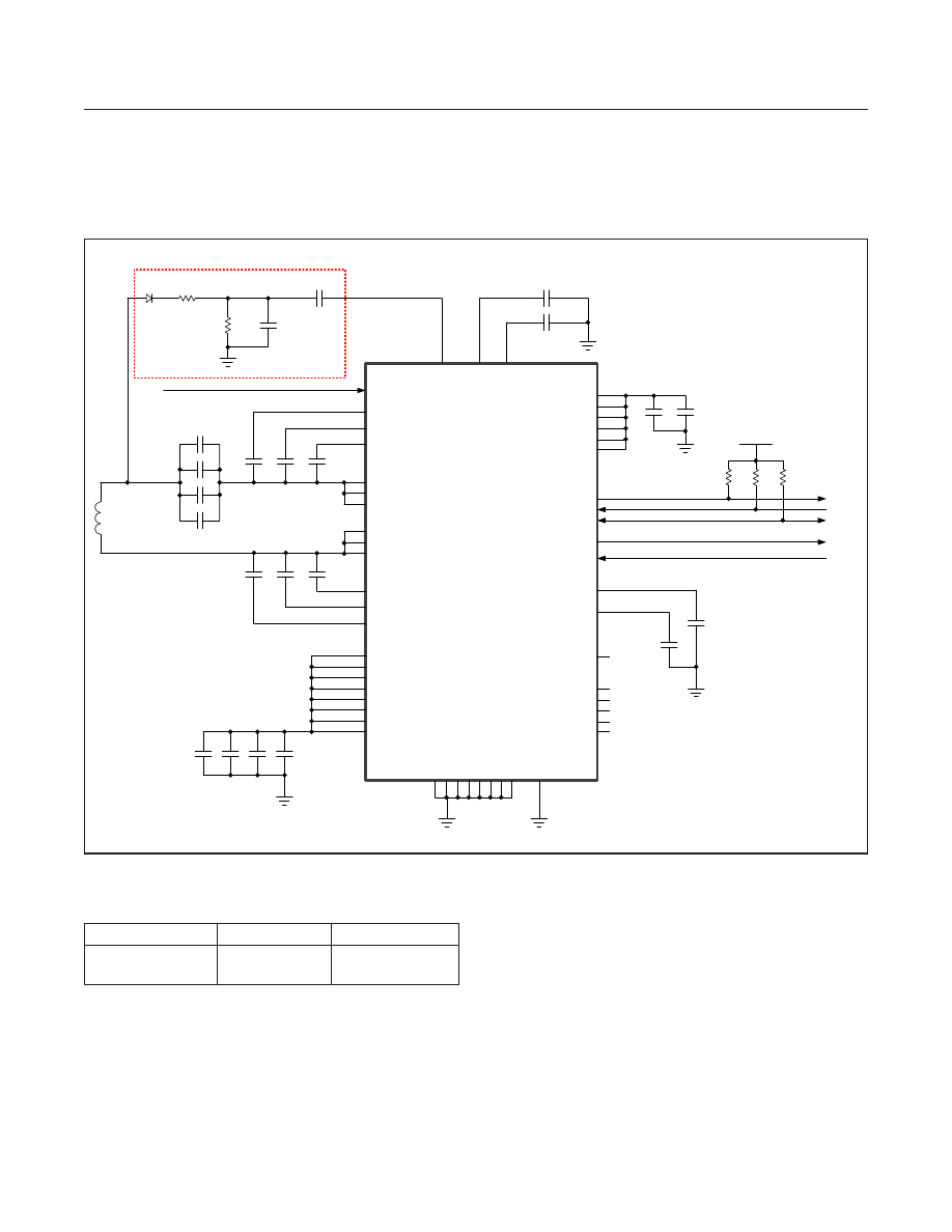
PART NUMBER
TEMP RANGE
PIN-PACKAGE
MAX77950EWW+T
-40 °C to +85 °C
52-bump WLP,
0.4mm pitch
+ Denotes a lead(Pb)-free/RoHS-compliant package.
T = Tape-and-reel.
DIS
WP_EN
CLAMP1
COMM1
BST1
AC1
AC1
AC1
AC2
AC2
AC2
BST2
COMM2
CLAMP2
V
RECT
V
RECT
V
RECT
V
RECT
V
RECT
V
RECT
V
RECT
G2
H1
H2
15nF
G1
A1
B1
B5
47nF
47nF
G5
H5
H6
DMODIN
100nF
100nF
100nF
100k٦
1nF
10nF
20k٦
GND
G
4
ADCREF
V
DD
Ls
8 µH
GND
1 µF
1 µF
V
RECT
V
OUT
V
OUT
V
OUT
V
OUT
V
OUT
V
OUT
INT
SCL
SDA
WP_DET
P2PEN
V1P8
V
CC
N.C.
DNC
DNC
DNC
DNC
DNC
C2
A2
H4
H3
G3
A5
GND
1 µF
1 µF
GND
D2
D3
D4
D5
D6
D1
10 µF
10 µF
100k٦ 2.2k٦ 2.2k٦
INT
SCL
SDA
VIO_SYSTEM
WP_DET
P2PEN
15nF
G6
A6
B6
47nF
47nF
PGND
PGND
PGND
PGND
PGND
PGND
PGND
PGND
AGND
GND
GND
C
1
C
6
J1
J2
J3
J4
J5
J6
B4
F6
F1
B2
C4
B3
A3
C3
10 µF
10 µF
10 µF 100nF
GND
E1
E2
F2
F3
F4
F5
E5
E6
A4
C
5
ONLY FOR PeerPower MODE
MAX77950
100nF
Typical Application Circuit
Ordering Information
www.maximintegrated.com
Maxim Integrated
52
MAX77950
WPC/PMA Dual Mode Wireless Power Receiver

REVISION
NUMBER
REVISION
DATE
DESCRIPTION
PAGES
CHANGED
0
3/17
Initial release
Revision History
Maxim Integrated cannot assume responsibility for use of any circuitry other than circuitry entirely embodied in a Maxim Integrated product. No circuit patent licenses
are implied. Maxim Integrated reserves the right to change the circuitry and specifications without notice at any time. The parametric values (min and max limits)
shown in the Electrical Characteristics table are guaranteed. Other parametric values quoted in this data sheet are provided for guidance.
Maxim Integrated and the Maxim Integrated logo are trademarks of Maxim Integrated Products, Inc.
© 2017 Maxim Integrated Products, Inc. 53
MAX77950
WPC/PMA Dual Mode Wireless Power Receiver
For pricing, delivery, and ordering information, please contact Maxim Direct at 1-888-629-4642, or visit Maxim Integrateds website at www.maximintegrated.com.