| Secciones |
|---|
| Foros Electrónica |
|
|
| Boletines de correo |
 |
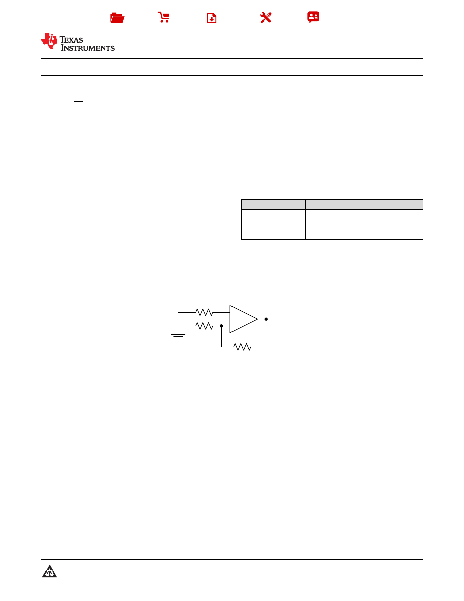
+
RIN
RG
RF
VOUT
VIN
, , ,
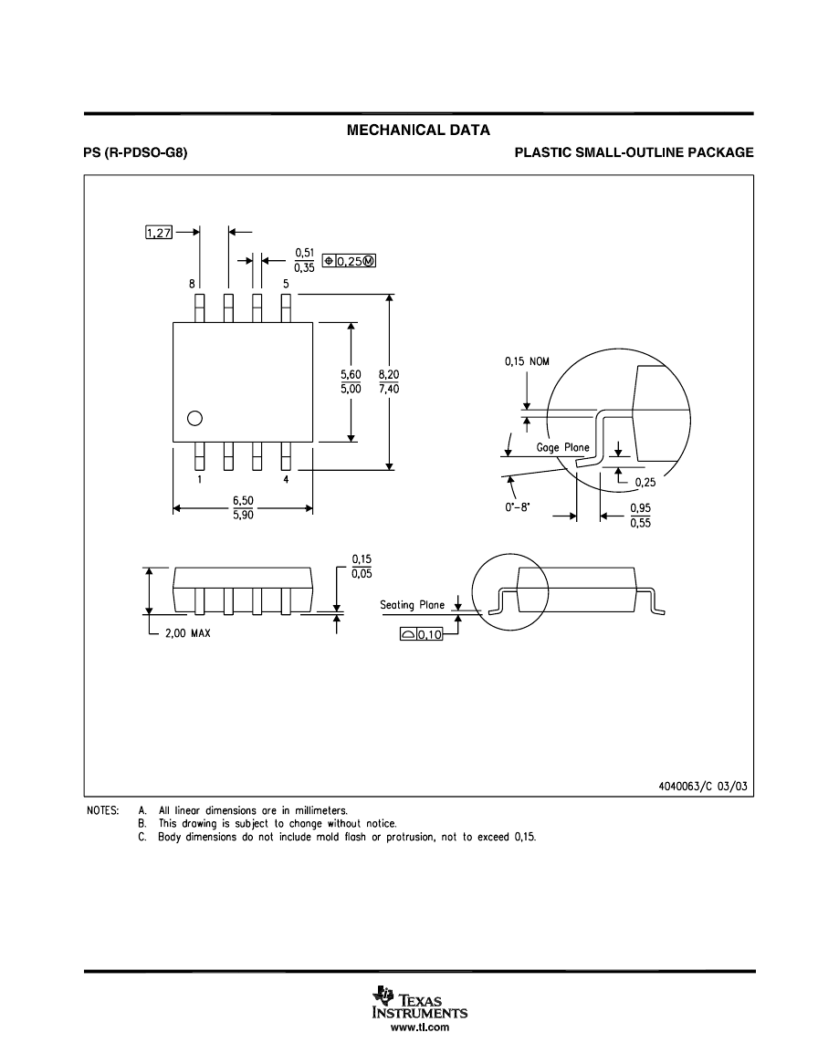
SLOS075J - NOVEMBER 1979 - REVISED JANUARY 2015
NE5532x, SA5532x Dual Low-Noise Operational Amplifiers
1 Features
3 Description
The NE5532, NE5532A, SA5532, and SA5532A
1
Equivalent Input Noise Voltage:
devices are high-performance operational amplifiers
5 nV/
√Hz Typ at 1 kHz
combining excellent DC and AC characteristics. They
Unity-Gain Bandwidth: 10 MHz Typ
feature very low noise, high output-drive capability,
Common-Mode Rejection Ratio: 100 dB Typ
high
unity-gain
and
maximum-output-swing
bandwidths, low distortion, high slew rate, input-
High DC Voltage Gain: 100 V/mV Typ
protection diodes, and output short-circuit protection.
Peak-to-Peak Output Voltage Swing 26 V Typ
These
operational
amplifiers
are
compensated
With V
CC ±
= ±15 V and R
L
= 600
Ω¦
internally for unity-gain operation. These devices
High Slew Rate: 9 V/
μs Typ
have specified maximum limits for equivalent input
noise voltage.
2 Applications
Device
AV Receivers
PART NUMBER
PACKAGE (PIN)
BODY SIZE (NOM)
Embedded PCs
NE5532x, SA5532x
SOIC (8)
4.90 mm × 3.91 mm
Netbooks
NE5532x, SA5532x
PDIP (8)
9.81 mm × 6.35 mm
Video Broadcasting and Infrastructure: Scalable
NE5532x
SO (8)
6.20 mm × 5.30 mm
Platforms
(1) For all available packages, see the orderable addendum at
DVD Recorders and Players
the end of the data sheet.
Multichannel Video Transcoders
Pro Audio Mixers
4 Simplified Schematic
1
An IMPORTANT NOTICE at the end of this data sheet addresses availability, warranty, changes, use in safety-critical applications,
intellectual property matters and other important disclaimers. PRODUCTION DATA.

, , ,
SLOS075J - NOVEMBER 1979 - REVISED JANUARY 2015
Table of Contents
8.2
Functional Block Diagram .........................................
1
Features ..................................................................
8.3
Feature Description...................................................
2
Applications ...........................................................
8.4
Device Functional Modes..........................................
3
Description .............................................................
9
Application and Implementation ..........................
4
Simplified Schematic.............................................
9.1
Typical Application ...................................................
5
Revision History.....................................................
10
Power Supply Recommendations .....................
6
Pin Configuration and Functions .........................
11
Layout...................................................................
7
Specifications.........................................................
11.1
Layout Guidelines .................................................
7.1
Absolute Maximum Ratings ......................................
11.2
Layout Example ....................................................
7.2
ESD Ratings..............................................................
12
Device and Documentation Support .................
7.3
Recommended Operating Conditions .......................
12.1
Related Links ........................................................
7.4
Thermal Information ..................................................
12.2
Trademarks ...........................................................
7.5
Electrical Characteristics...........................................
12.3
Electrostatic Discharge Caution ............................
7.6
Operating Characteristics..........................................
12.4
Glossary ................................................................
7.7
Typical Characteristics ..............................................
13
Mechanical, Packaging, and Orderable
8
Detailed Description ..............................................
Information ...........................................................
8.1
Overview ...................................................................
5 Revision History
Changes from Revision I (April 2009) to Revision J
Page
Added Applications, Device Information table, Pin Functions table, ESD Ratings table, Thermal Information table,
Typical Characteristics, Feature Description section, Device Functional Modes, Application and Implementation
section, Power Supply Recommendations section, Layout section, Device and Documentation Support section, and
Mechanical, Packaging, and Orderable Information section. .................................................................................................
Deleted Ordering Information table. .......................................................................................................................................
2
Copyright © 1979-2015, Texas Instruments Incorporated
Product Folder Links:

1
2
3
4
5
6
7
8
2IN+
2IN-
2OUT
V
CC+
V
CC-
1IN+
1IN-
1OUT
NE5532, NE5532A . . . D, P, OR PS PACKAGE
SA5532, SA5532A . . . D OR P PACKAGE
(TOP VIEW)
, , ,
SLOS075J - NOVEMBER 1979 - REVISED JANUARY 2015
6 Pin Configuration and Functions
Pin Functions
PIN
TYPE
DESCRIPTION
NAME
NO.
1IN+
3
I
Noninverting input
1IN-
2
I
Inverting Input
OUT1
1
O
Output
2IN+
5
I
Noninverting input
2IN-
6
I
Inverting Input
2OUT
7
O
Output
VCC+
8
Positive Supply
VCC-
4
Negative Supply
Copyright © 1979-2015, Texas Instruments Incorporated
3
Product Folder Links:
, , ,
SLOS075J - NOVEMBER 1979 - REVISED JANUARY 2015
7 Specifications
7.1 Absolute Maximum Ratings
over operating free-air temperature range (unless otherwise noted)
(1)
MIN
MAX
UNIT
V
CC+
0
22
V
V
CC
Supply voltage
(2)
V
CC-
-22
0
V
Input voltage, either input
(2) (3)
V
CC-
V
CC+
V
Input current
(4)
-10
10
mA
Duration of output short circuit
(5)
Unlimited
T
J
Operating virtual-junction temperature
150
°C
T
stg
Storage temperature range
-65
150
°C
(1)
Stresses beyond those listed under Absolute Maximum Ratings may cause permanent damage to the device. These are stress ratings
only, and functional operation of the device at these or any other conditions beyond those indicated under
is not implied. Exposure to absolute-maximum-rated conditions for extended periods may affect device reliability.
(2)
All voltage values, except differential voltages, are with respect to the midpoint between V
CC+
and V
CC-
.
(3)
The magnitude of the input voltage must never exceed the magnitude of the supply voltage.
(4)
Excessive input current will flow if a differential input voltage in excess of approximately 0.6 V is applied between the inputs, unless
some limiting resistance is used.
(5)
The output may be shorted to ground or either power supply. Temperature and/or supply voltages must be limited to ensure the
maximum dissipation rating is not exceeded.
7.2 ESD Ratings
VALUE
UNIT
Human body model (HBM), per ANSI/ESDA/JEDEC JS-001, all
2000
pins
(1)
V
(ESD)
Electrostatic discharge
V
Charged device model (CDM), per JEDEC specification JESD22-
1000
C101, all pins
(2)
(1)
JEDEC document JEP155 states that 500-V HBM allows safe manufacturing with a standard ESD control process.
(2)
JEDEC document JEP157 states that 250-V CDM allows safe manufacturing with a standard ESD control process.
7.3 Recommended Operating Conditions
MIN
MAX
UNIT
V
CC+
Supply voltage
5
15
V
V
CC-
Supply voltage
-5
-15
V
NE5532, NE5532A
0
70
T
A
Operating free-air temperature
°C
SA5532, SA5532A
-40
85
7.4 Thermal Information
NE5532, NE5532A, SA5532, and SA5532A
THERMAL METRIC
(1)
D
P
PS
UNIT
8 PINS
R
ΘJA
Junction-to-ambient thermal resistance
(2) (3)
97
85
95
°C/W
(1)
For more information about traditional and new thermal metrics, see the IC Package Thermal Metrics application report,
(2)
The package thermal impedance is calculated in accordance with JESD 51-7.
(3)
Maximum power dissipation is a function of T
J
(max),
Θ
JA
, and T
A
. The maximum allowable power dissipation at any allowable ambient
temperature is P
D
= (T
J
(max) - T
A
) /
Θ
JA.
Operating at the absolute maximum T
J
of 150 °C can affect reliability.
4
Copyright © 1979-2015, Texas Instruments Incorporated
Product Folder Links:
, , ,
SLOS075J - NOVEMBER 1979 - REVISED JANUARY 2015
7.5 Electrical Characteristics
V
CC ±
= ±15 V, T
A
= 25 °C (unless otherwise noted)
PARAMETER
TEST CONDITIONS
(1)
MIN
TYP
MAX
UNIT
T
A
= 25 °C
0.5
4
V
IO
Input offset voltage
V
O
= 0
mV
T
A
= Full range
(2)
5
T
A
= 25 °C
10
150
I
IO
Input offset current
nA
T
A
= Full range
(2)
200
T
A
= 25 °C
200
800
I
IB
Input bias current
nA
T
A
= Full range
(2)
1000
V
ICR
Common-mode input-voltage range
±12
±13
V
V
OPP
Maximum peak-to-peak output-voltage swing
R
L
≥ 600 Ω¦, V
CC ±
= ±15 V
24
26
V
T
A
= 25 °C
15
50
R
L
≥ 600 Ω¦, V
O
= ±10 V
T
A
= Full range
(2)
10
A
VD
Large-signal differential-voltage amplification
V/mV
T
A
= 25 °C
25
100
R
L
≥ 2 kΩ¦, V
O
±10 V
T
A
= Full range
(2)
15
A
vd
Small-signal differential-voltage amplification
f = 10 kHz
2.2
V/mV
B
OM
Maximum output-swing bandwidth
R
L
= 600
Ω¦, V
O
= ±10 V
140
kHz
B
1
Unity-gain bandwidth
R
L
= 600
Ω¦, C
L
= 100 pF
10
MHz
r
i
Input resistance
30
300
k
Ω¦
z
o
Output impedance
A
VD
= 30 dB, R
L
= 600
Ω¦, f = 10 kHz
0.3
Ω¦
CMRR Common-mode rejection ratio
V
IC
= V
ICR
min
70
100
dB
k
SVR
Supply-voltage rejection ratio (
ΔV
CC ±
/
ΔV
IO
)
V
CC ±
= ±9 V to ±15 V, V
O
= 0
80
100
dB
I
OS
Output short-circuit current
10
38
60
mA
I
CC
Total supply current
V
O
= 0, No load
8
16
mA
Crosstalk attenuation (V
O1
/V
O2
)
V
01
= 10 V peak, f = 1 kHz
110
dB
(1)
All characteristics are measured under open-loop conditions, with zero common-mode input voltage, unless otherwise specified.
(2)
Full temperature ranges are: -40 °C to 85 °C for the SA5532 and SA5532A devices, and 0 °C to 70 °C for the NE5532 and NE5532A
devices.
7.6 Operating Characteristics
V
CC ±
= ±15 V, T
A
= 25 °C (unless otherwise noted)
NE5532, SA5532
NE5532A, SA5532A
PARAMETER
TEST CONDITIONS
UNIT
MIN
TYP
MAX
MIN
TYP
MAX
SR
Slew rate at unity gain
9
9
V/
μs
V
I
= 100 mV,
R
L
= 600
Ω¦,
Overshoot factor
10
10
%
A
VD
= 1,
C
L
= 100 pF
f = 30 Hz
8
8
10
V
n
Equivalent input noise voltage
nV/
√Hz
f = 1 kHz
5
5
6
f = 30 Hz
2.7
2.7
I
n
Equivalent input noise current
pA/
√Hz
f = 1 kHz
0.7
0.7
Copyright © 1979-2015, Texas Instruments Incorporated
5
Product Folder Links:
Temperature (C)
Ou
tp
u
t S
w
in
g
B
a
n
d
w
id
th
(k
H
z
)
-40
-20
0
20
40
60
80
100
0
20
40
60
80
100
120
140
160
180
D003
Frequency (Hz)
E
q
u
iv
a
le
n
t i
n
p
u
t n
o
is
e
V
o
lta
g
e
(
n
V
)
10
100
1000
10000
100000
0
2
4
6
8
10
12
14
16
18
D001
Frequency (Hz)
E
q
u
iv
a
le
n
t i
n
p
u
t n
o
is
e
c
u
rre
n
t (p
A
)
10
100
1000
0
0.2
0.4
0.6
0.8
1
1.2
1.4
1.6
D002
, , ,
SLOS075J - NOVEMBER 1979 - REVISED JANUARY 2015
7.7 Typical Characteristics
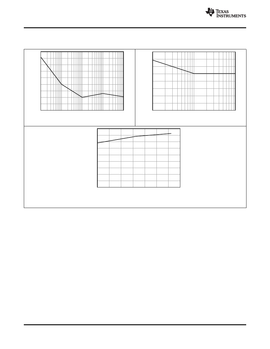
Figure 1. Equivalent Input Noise Voltage vs Frequency
Figure 2. Equivalent Input Noise Current vs Frequency
Figure 3. Output Swing Bandwidth
vs Temperature at V
CC
= ±10 V
6
Copyright © 1979-2015, Texas Instruments Incorporated
Product Folder Links:
OUT
V
CC-
V
CC+
36 pF
37 pF
14 pF
7 pF
15 W
460 W
15 W
IN+
IN-
Component values shown are nominal.
, , ,
SLOS075J - NOVEMBER 1979 - REVISED JANUARY 2015
8 Detailed Description
8.1 Overview
The NE5532, NE5532A, SA5532, and SA5532A devices are high-performance operational amplifiers combining
excellent dc and ac characteristics. They feature very low noise, high output-drive capability, high unity-gain and
maximum-output-swing bandwidths, low distortion, high slew rate, input-protection diodes, and output short-
circuit protection. These operational amplifiers are compensated internally for unity-gain operation. These
devices have specified maximum limits for equivalent input noise voltage.
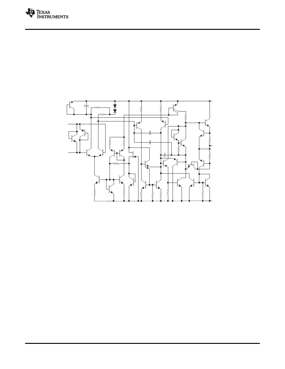
8.2 Functional Block Diagram
8.3 Feature Description
8.3.1 Unity-Gain Bandwidth
The unity-gain bandwidth is the frequency up to which an amplifier with a unity gain may be operated without
greatly distorting the signal. The NE5532, NE5532A, SA5532, and SA5532A devices have a 10-MHz unity-gain
bandwidth.
8.3.2 Common-Mode Rejection Ratio
The common-mode rejection ratio (CMRR) of an amplifier is a measure of how well the device rejects unwanted
input signals common to both input leads. It is found by taking the ratio of the change in input offset voltage to
the change in the input voltage and converting to decibels. Ideally the CMRR would be infinite, but in practice,
amplifiers are designed to have it as high as possible. The CMRR of the NE5532, NE5532A, SA5532, and
SA5532A devices is 100 dB.
8.3.3 Slew Rate
The slew rate is the rate at which an operational amplifier can change its output when there is a change on the
input. The NE5532, NE5532A, SA5532, and SA5532A devices have a 9-V/ms slew rate.
8.4 Device Functional Modes
The NE5532, NE5532A, SA5532, and SA5532A devices are powered on when the supply is connected. Each of
these devices can be operated as a single supply operational amplifier or dual supply amplifier depending on the
application.
Copyright © 1979-2015, Texas Instruments Incorporated
7
Product Folder Links:
R
3
R
1
R
2
R
4
15 V
V
REF
12 V
+
+
V
IN
+
V
DIFF
±
V
OUT-
V
OUT+
, , ,
SLOS075J - NOVEMBER 1979 - REVISED JANUARY 2015
9 Application and Implementation
NOTE
Information in the following applications sections is not part of the TI component
specification, and TI does not warrant its accuracy or completeness. TIs customers are
responsible for determining suitability of components for their purposes. Customers should
validate and test their design implementation to confirm system functionality.
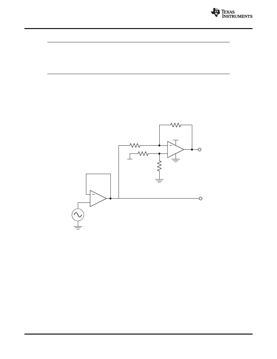
9.1 Typical Application
Some applications require differential signals.
shows a simple circuit to convert a single-ended input of 2
V to 10 V into differential output of ±8 V on a single 15-V supply. The output range is intentionally limited to
maximize linearity. The circuit is composed of two amplifiers. One amplifier acts as a buffer and creates a
voltage, V
OUT+
. The second amplifier inverts the input and adds a reference voltage to generate V
OUT-
. Both
V
OUT+
and V
OUT-
range from 2 V to 10 V. The difference, V
DIFF
, is the difference between V
OUT+
and V
OUT-
.
Figure 4. Schematic for Single-Ended Input to Differential Output Conversion
9.1.1 Design Requirements
The design requirements are as follows:
Supply voltage: 15 V
Reference voltage: 12V
Input: 2 V to 10 V
Output differential: ±8 V
8
Copyright © 1979-2015, Texas Instruments Incorporated
Product Folder Links:
OUT
OUT
cm
REF
V
V
1
V
V
2
2
+
-
+
æ
ö
=
=
ç
÷
è
ø
2
4
2
D IF F
O U T
O U T
IN
R E F
1
3
4
1
R
R
R
V
V
V
V
1
V
1
R
R
R
R
+
-
æ
ö
æ
ö
æ
ö
=
-
=
´
+
-
´
+
ç
÷
ç
÷
ç
÷
+
è
ø
è
ø
è
ø
4
2
2
out
ref
in
3
4
1
1
R
R
R
V
V
1
V
R
R
R
R
-
æ
ö æ
ö
=
´
´
+
-
´
ç
÷ ç
÷
+
è
ø
è
ø
, , ,
SLOS075J - NOVEMBER 1979 - REVISED JANUARY 2015
Typical Application (continued)
9.1.2 Detailed Design Procedure
The circuit in
takes a single-ended input signal, V
IN
, and generates two output signals, V
OUT+
and V
OUT-
using two amplifiers and a reference voltage, V
REF
. V
OUT+
is the output of the first amplifier and is a buffered
version of the input signal, V
IN
. V
OUT-
is the output of the second amplifier which uses V
REF
to add an
offset voltage to V
IN
and feedback to add inverting gain. The transfer function for V
OUT-
is
.
V
OUT+
= V
IN
(1)
(2)
The differential output signal, V
DIFF
, is the difference between the two single-ended output signals, V
OUT+
and
V
OUT-
.
shows the transfer function for V
DIFF
. By applying the conditions that R
1
= R
2
and R
3
= R
4
, the
transfer function is simplified into
Using this configuration, the maximum input signal is equal to the
reference voltage and the maximum output of each amplifier is equal to the V
REF
. The differential output range is
2×V
REF
. Furthermore, the common mode voltage will be one half of V
REF
(see
(3)
V
OUT+
= V
IN
(4)
V
OUT-
= V
REF
- V
IN
(5)
V
DIFF
= 2×V
IN
- V
REF
(6)
(7)
9.1.2.1 Amplifier Selection
Linearity over the input range is key for good dc accuracy. The common mode input range and the output swing
limitations determine the linearity. In general, an amplifier with rail-to-rail input and output swing is required.
Bandwidth is a key concern for this design. Since the NE5532 has a bandwidth of 10 MHz, this circuit will only be
able to process signals with frequencies of less than 10 MHz.
9.1.2.2 Passive Component Selection
Because the transfer function of V
OUT-
is heavily reliant on resistors (R
1
, R
2
, R
3
, and R
4
), use resistors with low
tolerances to maximize performance and minimize error. This design used resistors with resistance values of 36
k
Ω with tolerances measured to be within 2%. But, if the noise of the system is a key parameter, the user can
select smaller resistance values (6 k
Ω or lower) to keep the overall system noise low. This ensures that the noise
from the resistors is lower than the amplifier noise.
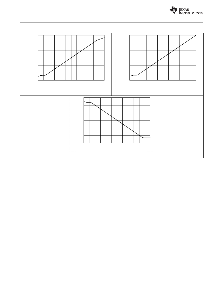
9.1.3 Application Curves
The measured transfer functions in
,
, and
were generated by sweeping the input
voltage from 0 V to 12V. However, this design should only be used between 2 V and 10 V for optimum linearity.
Copyright © 1979-2015, Texas Instruments Incorporated
9
Product Folder Links:
0
2
4
6
8
10
12
0
1
2
3
4
5
6
7
8
9
10
11
12
V
OUT
t
(
V
)
VIN (V)
C002
±
12
±
8
±
4
0
4
8
12
0
1
2
3
4
5
6
7
8
9
10
11
12
V
DI
F
F
(
V
)
VIN (V)
C003
0
2
4
6
8
10
12
0
1
2
3
4
5
6
7
8
9
10
11
12
V
OUT
+ (
V
)
VIN (V)
C001
, , ,
SLOS075J - NOVEMBER 1979 - REVISED JANUARY 2015
Typical Application (continued)
Figure 5. Differential Output Voltage vs Input Voltage
Figure 6. Positive Output Voltage Node vs Input Voltage
Figure 7. Positive Output Voltage Node vs Input Voltage
10
Copyright © 1979-2015, Texas Instruments Incorporated
Product Folder Links:
+
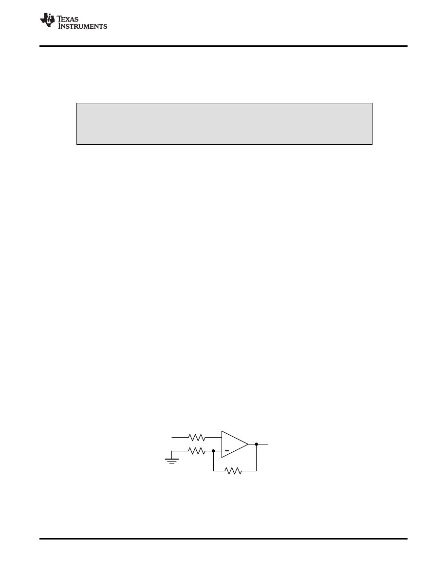
RIN
RG
RF
VOUT
VIN
, , ,
SLOS075J - NOVEMBER 1979 - REVISED JANUARY 2015
10 Power Supply Recommendations
The NE5532x and SA5532x devices are specified for operation over the range of ±5 to ±15 V; many
specifications apply from 0 °C to 70 °C (NE5532x) and -40 °C to 85 °C (SA5532x). The
section presents parameters that can exhibit significant variance with regard to operating voltage or temperature.
CAUTION
Supply voltages outside of the ±22 V range can permanently damage the device (see
the
Place 0.1-
μF bypass capacitors close to the power-supply pins to reduce errors coupling in from noisy or high
impedance power supplies. For more detailed information on bypass capacitor placement, refer to the
11 Layout
11.1 Layout Guidelines
For best operational performance of the device, use good PCB layout practices, including:
Noise can propagate into analog circuitry through the power pins of the circuit as a whole and the operational
amplifier. Bypass capacitors are used to reduce the coupled noise by providing low impedance power
sources local to the analog circuitry.
-
Connect low-ESR, 0.1-
μF ceramic bypass capacitors between each supply pin and ground, placed as
close to the device as possible. A single bypass capacitor from V+ to ground is applicable for single
supply applications.
Separate grounding for analog and digital portions of circuitry is one of the simplest and most-effective
methods of noise suppression. One or more layers on multilayer PCBs are usually devoted to ground planes.
A ground plane helps distribute heat and reduces EMI noise pickup. Make sure to physically separate digital
and analog grounds, paying attention to the flow of the ground current. For more detailed information, refer to
Circuit Board Layout Techniques,
To reduce parasitic coupling, run the input traces as far away from the supply or output traces as possible. If
it is not possible to keep them separate, it is much better to cross the sensitive trace perpendicular as
opposed to in parallel with the noisy trace.
Place the external components as close to the device as possible. Keeping RF and RG close to the inverting
input minimizes parasitic capacitance, as shown in
Keep the length of input traces as short as possible. Always remember that the input traces are the most
sensitive part of the circuit.
Consider a driven, low-impedance guard ring around the critical traces. A guard ring can significantly reduce
leakage currents from nearby traces that are at different potentials.
11.2 Layout Example
Figure 8. Operational Amplifier Schematic for Noninverting Configuration
Copyright © 1979-2015, Texas Instruments Incorporated
11
Product Folder Links:
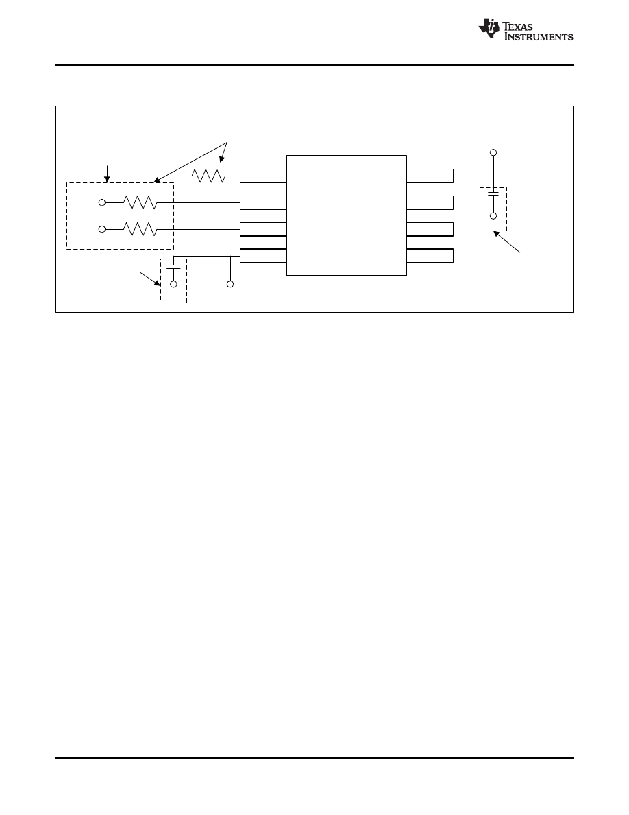
OUT1
OUT2
IN1
Ã
IN1+
VCC
Ã
VCC+
IN2
Ã
IN2+
RG
RIN
RF
GND
VIN
VS-
GND
VS+
GND
Run the input traces as far
away from the supply lines
as possible
Only needed for
dual-supply
operation
Place components close to
device and to each other to
reduce parasitic errors
Use low-ESR, ceramic
bypass capacitor
(or GND for single supply)
Ground (GND) plane on another layer
, , ,
SLOS075J - NOVEMBER 1979 - REVISED JANUARY 2015
Layout Example (continued)
Figure 9. Operational Amplifier Board Layout for Noninverting Configuration
12
Copyright © 1979-2015, Texas Instruments Incorporated
Product Folder Links:
, , ,
SLOS075J - NOVEMBER 1979 - REVISED JANUARY 2015
12 Device and Documentation Support
12.1 Related Links
The table below lists quick access links. Categories include technical documents, support and community
resources, tools and software, and quick access to sample or buy.
Table 1. Related Links
Technical
Support &
Parts
Product Folder
Sample & Buy
Tools & Software
Documents
Community
NE5532
NE5532A
SA5532
SA5532A
12.2 Trademarks
All trademarks are the property of their respective owners.
12.3 Electrostatic Discharge Caution
This integrated circuit can be damaged by ESD. Texas Instruments recommends that all integrated circuits be handled with
appropriate precautions. Failure to observe proper handling and installation procedures can cause damage.
ESD damage can range from subtle performance degradation to complete device failure. Precision integrated circuits may be more
susceptible to damage because very small parametric changes could cause the device not to meet its published specifications.
12.4 Glossary
TI Glossary.
This glossary lists and explains terms, acronyms and definitions.
13 Mechanical, Packaging, and Orderable Information
The following pages include mechanical packaging and orderable information. This information is the most
current data available for the designated devices. This data is subject to change without notice and revision of
this document. For browser based versions of this data sheet, refer to the left hand navigation.
Copyright © 1979-2015, Texas Instruments Incorporated
13
Product Folder Links:
PACKAGE OPTION ADDENDUM
www.ti.com
17-Dec-2015
Addendum-Page 1
PACKAGING INFORMATION
Orderable Device
Status
(1)
Package Type Package
Drawing
Pins Package
Qty
Eco Plan
(2)
Lead/Ball Finish
(6)
MSL Peak Temp
(3)
Op Temp ( °C)
Device Marking
(4/5)
Samples
NE5532AD
ACTIVE
SOIC
D
8
75
Green (RoHS
& no Sb/Br)
CU NIPDAU
Level-1-260C-UNLIM
0 to 70
N5532A
NE5532ADE4
ACTIVE
SOIC
D
8
75
Green (RoHS
& no Sb/Br)
CU NIPDAU
Level-1-260C-UNLIM
0 to 70
N5532A
NE5532ADR
ACTIVE
SOIC
D
8
2500
Green (RoHS
& no Sb/Br)
CU NIPDAU
Level-1-260C-UNLIM
0 to 70
N5532A
NE5532ADRE4
ACTIVE
SOIC
D
8
2500
Green (RoHS
& no Sb/Br)
CU NIPDAU
Level-1-260C-UNLIM
0 to 70
N5532A
NE5532ADRG4
ACTIVE
SOIC
D
8
2500
Green (RoHS
& no Sb/Br)
CU NIPDAU
Level-1-260C-UNLIM
0 to 70
N5532A
NE5532AIP
OBSOLETE
PDIP
P
8
TBD
Call TI
Call TI
-40 to 85
NE5532AP
ACTIVE
PDIP
P
8
50
Pb-Free
(RoHS)
CU NIPDAU
N / A for Pkg Type
0 to 70
NE5532AP
NE5532APE4
ACTIVE
PDIP
P
8
50
Pb-Free
(RoHS)
CU NIPDAU
N / A for Pkg Type
0 to 70
NE5532AP
NE5532APSR
ACTIVE
SO
PS
8
2000
Green (RoHS
& no Sb/Br)
CU NIPDAU
Level-1-260C-UNLIM
0 to 70
N5532A
NE5532APSRE4
ACTIVE
SO
PS
8
2000
Green (RoHS
& no Sb/Br)
CU NIPDAU
Level-1-260C-UNLIM
0 to 70
N5532A
NE5532D
ACTIVE
SOIC
D
8
75
Green (RoHS
& no Sb/Br)
CU NIPDAU
Level-1-260C-UNLIM
0 to 70
N5532
NE5532DG4
ACTIVE
SOIC
D
8
75
Green (RoHS
& no Sb/Br)
CU NIPDAU
Level-1-260C-UNLIM
0 to 70
N5532
NE5532DR
ACTIVE
SOIC
D
8
2500
Green (RoHS
& no Sb/Br)
CU NIPDAU | CU SN
Level-1-260C-UNLIM
0 to 70
N5532
NE5532DRE4
ACTIVE
SOIC
D
8
2500
Green (RoHS
& no Sb/Br)
CU NIPDAU
Level-1-260C-UNLIM
0 to 70
N5532
NE5532DRG4
ACTIVE
SOIC
D
8
2500
Green (RoHS
& no Sb/Br)
CU NIPDAU
Level-1-260C-UNLIM
0 to 70
N5532
NE5532IP
OBSOLETE
PDIP
P
8
TBD
Call TI
Call TI
-40 to 85
NE5532P
ACTIVE
PDIP
P
8
50
Pb-Free
(RoHS)
CU NIPDAU | CU SN
N / A for Pkg Type
0 to 70
NE5532P
NE5532PE4
ACTIVE
PDIP
P
8
50
Pb-Free
(RoHS)
CU NIPDAU
N / A for Pkg Type
0 to 70
NE5532P

PACKAGE OPTION ADDENDUM
www.ti.com
17-Dec-2015
Addendum-Page 2
Orderable Device
Status
(1)
Package Type Package
Drawing
Pins Package
Qty
Eco Plan
(2)
Lead/Ball Finish
(6)
MSL Peak Temp
(3)
Op Temp ( °C)
Device Marking
(4/5)
Samples
NE5532PSR
ACTIVE
SO
PS
8
2000
Green (RoHS
& no Sb/Br)
CU NIPDAU
Level-1-260C-UNLIM
0 to 70
N5532
NE5532PSRE4
ACTIVE
SO
PS
8
2000
Green (RoHS
& no Sb/Br)
CU NIPDAU
Level-1-260C-UNLIM
0 to 70
N5532
NE5532PSRG4
ACTIVE
SO
PS
8
2000
Green (RoHS
& no Sb/Br)
CU NIPDAU
Level-1-260C-UNLIM
0 to 70
N5532
SA5532AD
ACTIVE
SOIC
D
8
75
Green (RoHS
& no Sb/Br)
CU NIPDAU
Level-1-260C-UNLIM
-40 to 85
SA5532A
SA5532ADG4
ACTIVE
SOIC
D
8
75
Green (RoHS
& no Sb/Br)
CU NIPDAU
Level-1-260C-UNLIM
-40 to 85
SA5532A
SA5532ADR
ACTIVE
SOIC
D
8
2500
Green (RoHS
& no Sb/Br)
CU NIPDAU
Level-1-260C-UNLIM
-40 to 85
SA5532A
SA5532ADRG4
ACTIVE
SOIC
D
8
2500
Green (RoHS
& no Sb/Br)
CU NIPDAU
Level-1-260C-UNLIM
-40 to 85
SA5532A
SA5532AP
ACTIVE
PDIP
P
8
50
Pb-Free
(RoHS)
CU NIPDAU
N / A for Pkg Type
-40 to 85
SA5532AP
SA5532APE4
ACTIVE
PDIP
P
8
50
Pb-Free
(RoHS)
CU NIPDAU
N / A for Pkg Type
-40 to 85
SA5532AP
SA5532D
ACTIVE
SOIC
D
8
75
Green (RoHS
& no Sb/Br)
CU NIPDAU
Level-1-260C-UNLIM
-40 to 85
SA5532
SA5532DR
ACTIVE
SOIC
D
8
2500
Green (RoHS
& no Sb/Br)
CU NIPDAU
Level-1-260C-UNLIM
-40 to 85
SA5532
SA5532DRG4
ACTIVE
SOIC
D
8
2500
Green (RoHS
& no Sb/Br)
CU NIPDAU
Level-1-260C-UNLIM
-40 to 85
SA5532
SA5532P
ACTIVE
PDIP
P
8
50
Pb-Free
(RoHS)
CU NIPDAU
N / A for Pkg Type
-40 to 85
SA5532P
SA5532PE4
ACTIVE
PDIP
P
8
50
Pb-Free
(RoHS)
CU NIPDAU
N / A for Pkg Type
-40 to 85
SA5532P
(1)
The marketing status values are defined as follows:
ACTIVE: Product device recommended for new designs.
LIFEBUY: TI has announced that the device will be discontinued, and a lifetime-buy period is in effect.
NRND: Not recommended for new designs. Device is in production to support existing customers, but TI does not recommend using this part in a new design.
PREVIEW: Device has been announced but is not in production. Samples may or may not be available.
OBSOLETE: TI has discontinued the production of the device.
PACKAGE OPTION ADDENDUM
www.ti.com
17-Dec-2015
Addendum-Page 3
(2)
Eco Plan - The planned eco-friendly classification: Pb-Free (RoHS), Pb-Free (RoHS Exempt), or Green (RoHS & no Sb/Br) - please check
for the latest availability
information and additional product content details.
TBD: The Pb-Free/Green conversion plan has not been defined.
Pb-Free (RoHS): TI's terms "Lead-Free" or "Pb-Free" mean semiconductor products that are compatible with the current RoHS requirements for all 6 substances, including the requirement that
lead not exceed 0.1% by weight in homogeneous materials. Where designed to be soldered at high temperatures, TI Pb-Free products are suitable for use in specified lead-free processes.
Pb-Free (RoHS Exempt): This component has a RoHS exemption for either 1) lead-based flip-chip solder bumps used between the die and package, or 2) lead-based die adhesive used between
the die and leadframe. The component is otherwise considered Pb-Free (RoHS compatible) as defined above.
Green (RoHS & no Sb/Br): TI defines "Green" to mean Pb-Free (RoHS compatible), and free of Bromine (Br) and Antimony (Sb) based flame retardants (Br or Sb do not exceed 0.1% by weight
in homogeneous material)
(3)
MSL, Peak Temp. - The Moisture Sensitivity Level rating according to the JEDEC industry standard classifications, and peak solder temperature.
(4)
There may be additional marking, which relates to the logo, the lot trace code information, or the environmental category on the device.
(5)
Multiple Device Markings will be inside parentheses. Only one Device Marking contained in parentheses and separated by a "~" will appear on a device. If a line is indented then it is a continuation
of the previous line and the two combined represent the entire Device Marking for that device.
(6)
Lead/Ball Finish - Orderable Devices may have multiple material finish options. Finish options are separated by a vertical ruled line. Lead/Ball Finish values may wrap to two lines if the finish
value exceeds the maximum column width.
Important Information and Disclaimer:The information provided on this page represents TI's knowledge and belief as of the date that it is provided. TI bases its knowledge and belief on information
provided by third parties, and makes no representation or warranty as to the accuracy of such information. Efforts are underway to better integrate information from third parties. TI has taken and
continues to take reasonable steps to provide representative and accurate information but may not have conducted destructive testing or chemical analysis on incoming materials and chemicals.
TI and TI suppliers consider certain information to be proprietary, and thus CAS numbers and other limited information may not be available for release.
In no event shall TI's liability arising out of such information exceed the total purchase price of the TI part(s) at issue in this document sold by TI to Customer on an annual basis.
TAPE AND REEL INFORMATION
*All dimensions are nominal
Device
Package
Type
Package
Drawing
Pins
SPQ
Reel
Diameter
(mm)
Reel
Width
W1 (mm)
A0
(mm)
B0
(mm)
K0
(mm)
P1
(mm)
W
(mm)
Pin1
Quadrant
NE5532ADR
SOIC
D
8
2500
330.0
12.4
6.4
5.2
2.1
8.0
12.0
Q1
NE5532APSR
SO
PS
8
2000
330.0
16.4
8.2
6.6
2.5
12.0
16.0
Q1
NE5532DR
SOIC
D
8
2500
330.0
12.4
6.4
5.2
2.1
8.0
12.0
Q1
NE5532DR
SOIC
D
8
2500
330.0
12.8
6.4
5.2
2.1
8.0
12.0
Q1
NE5532DRG4
SOIC
D
8
2500
330.0
12.4
6.4
5.2
2.1
8.0
12.0
Q1
NE5532PSR
SO
PS
8
2000
330.0
16.4
8.2
6.6
2.5
12.0
16.0
Q1
SA5532ADR
SOIC
D
8
2500
330.0
12.4
6.4
5.2
2.1
8.0
12.0
Q1
SA5532DR
SOIC
D
8
2500
330.0
12.4
6.4
5.2
2.1
8.0
12.0
Q1
PACKAGE MATERIALS INFORMATION
www.ti.com
21-Jan-2014
Pack Materials-Page 1
*All dimensions are nominal
Device
Package Type
Package Drawing
Pins
SPQ
Length (mm)
Width (mm)
Height (mm)
NE5532ADR
SOIC
D
8
2500
340.5
338.1
20.6
NE5532APSR
SO
PS
8
2000
367.0
367.0
38.0
NE5532DR
SOIC
D
8
2500
340.5
338.1
20.6
NE5532DR
SOIC
D
8
2500
364.0
364.0
27.0
NE5532DRG4
SOIC
D
8
2500
340.5
338.1
20.6
NE5532PSR
SO
PS
8
2000
367.0
367.0
38.0
SA5532ADR
SOIC
D
8
2500
340.5
338.1
20.6
SA5532DR
SOIC
D
8
2500
340.5
338.1
20.6
PACKAGE MATERIALS INFORMATION
www.ti.com
21-Jan-2014
Pack Materials-Page 2

IMPORTANT NOTICE
Texas Instruments Incorporated and its subsidiaries (TI) reserve the right to make corrections, enhancements, improvements and other
changes to its semiconductor products and services per JESD46, latest issue, and to discontinue any product or service per JESD48, latest
issue. Buyers should obtain the latest relevant information before placing orders and should verify that such information is current and
complete. All semiconductor products (also referred to herein as components) are sold subject to TIs terms and conditions of sale
supplied at the time of order acknowledgment.
TI warrants performance of its components to the specifications applicable at the time of sale, in accordance with the warranty in TIs terms
and conditions of sale of semiconductor products. Testing and other quality control techniques are used to the extent TI deems necessary
to support this warranty. Except where mandated by applicable law, testing of all parameters of each component is not necessarily
performed.
TI assumes no liability for applications assistance or the design of Buyers products. Buyers are responsible for their products and
applications using TI components. To minimize the risks associated with Buyers products and applications, Buyers should provide
adequate design and operating safeguards.
TI does not warrant or represent that any license, either express or implied, is granted under any patent right, copyright, mask work right, or
other intellectual property right relating to any combination, machine, or process in which TI components or services are used. Information
published by TI regarding third-party products or services does not constitute a license to use such products or services or a warranty or
endorsement thereof. Use of such information may require a license from a third party under the patents or other intellectual property of the
third party, or a license from TI under the patents or other intellectual property of TI.
Reproduction of significant portions of TI information in TI data books or data sheets is permissible only if reproduction is without alteration
and is accompanied by all associated warranties, conditions, limitations, and notices. TI is not responsible or liable for such altered
documentation. Information of third parties may be subject to additional restrictions.
Resale of TI components or services with statements different from or beyond the parameters stated by TI for that component or service
voids all express and any implied warranties for the associated TI component or service and is an unfair and deceptive business practice.
TI is not responsible or liable for any such statements.
Buyer acknowledges and agrees that it is solely responsible for compliance with all legal, regulatory and safety-related requirements
concerning its products, and any use of TI components in its applications, notwithstanding any applications-related information or support
that may be provided by TI. Buyer represents and agrees that it has all the necessary expertise to create and implement safeguards which
anticipate dangerous consequences of failures, monitor failures and their consequences, lessen the likelihood of failures that might cause
harm and take appropriate remedial actions. Buyer will fully indemnify TI and its representatives against any damages arising out of the use
of any TI components in safety-critical applications.
In some cases, TI components may be promoted specifically to facilitate safety-related applications. With such components, TIs goal is to
help enable customers to design and create their own end-product solutions that meet applicable functional safety standards and
requirements. Nonetheless, such components are subject to these terms.
No TI components are authorized for use in FDA Class III (or similar life-critical medical equipment) unless authorized officers of the parties
have executed a special agreement specifically governing such use.
Only those TI components which TI has specifically designated as military grade or enhanced plastic are designed and intended for use in
military/aerospace applications or environments. Buyer acknowledges and agrees that any military or aerospace use of TI components
which have not been so designated is solely at the Buyer's risk, and that Buyer is solely responsible for compliance with all legal and
regulatory requirements in connection with such use.
TI has specifically designated certain components as meeting ISO/TS16949 requirements, mainly for automotive use. In any case of use of
non-designated products, TI will not be responsible for any failure to meet ISO/TS16949.
Products
Applications
Audio
Automotive and Transportation
Amplifiers
Communications and Telecom
Data Converters
Computers and Peripherals
DLP ® Products
Consumer Electronics
DSP
Energy and Lighting
Clocks and Timers
Industrial
Interface
Medical
Logic
Security
Power Mgmt
Space, Avionics and Defense
Microcontrollers
Video and Imaging
RFID
OMAP Applications Processors
TI E2E Community
Wireless Connectivity
Mailing Address: Texas Instruments, Post Office Box 655303, Dallas, Texas 75265
Copyright © 2015, Texas Instruments Incorporated
Document Outline

