| Secciones |
|---|
| Foros Electrónica |
|
|
| Boletines de correo |
 |

IN-
COMP/BAL
COMP
OUT
BALANCE
-
+
IN+
, , ,
SLOS070D - JULY 1979 - REVISED NOVEMBER 2014
NE5534x, SA5534x Low-Noise Operational Amplifiers
1 Features
3 Description
The NE5534, NE5534A, SA5534, and SA5534A
1
Equivalent Input Noise Voltage
devices are high-performance operational amplifiers
3.5 nV/
√Hz Typ
combining excellent dc and ac characteristics. Some
Unity-Gain Bandwidth 10 MHz Typ
of the features include very low noise, high output-
Common-Mode Rejection Ratio 100 dB Typ
drive capability, high unity-gain and maximum-output-
swing bandwidths, low distortion, and high slew rate.
High DC Voltage Gain 100 V/mV Typ
Peak-to-Peak Output Voltage Swing 32 V Typ
These
operational
amplifiers
are
compensated
internally for a gain equal to or greater than three.
With V
CC ±
= ±18 V and R
L
= 600
Ω¦
Optimization of the frequency response for various
High Slew Rate 13 V/
μs Typ
applications can be obtained by use of an external
Wide Supply-Voltage Range ±3 V to ±20 V
compensation
capacitor
between
COMP
and
Low Harmonic Distortion
COMP/BAL. The devices feature input-protection
diodes, output short-circuit protection, and offset-
Offset Nulling Capability
voltage nulling capability with use of the BALANCE
External Compensation Capability
and COMP/BAL pins (see
For the NE5534A and SA5534A devices, a maximum
2 Applications
limit is specified for the equivalent input noise
Audio Preamplifiers
voltage.
Servo Error Amplifiers
Device Information
Medical Equipment
PART NUMBER
PACKAGE (PIN)
BODY SIZE (NOM)
Telephone Channel Amplifiers
NE5534x
SOIC (8)
4.90 mm × 3.91 mm
SOIC (8)
4.90 mm × 3.91 mm
SA5534x
SO (8)
6.20 mm × 5.30 mm
4 Simplified Schematic
1
An IMPORTANT NOTICE at the end of this data sheet addresses availability, warranty, changes, use in safety-critical applications,
intellectual property matters and other important disclaimers. PRODUCTION DATA.

, , ,
SLOS070D - JULY 1979 - REVISED NOVEMBER 2014
Table of Contents
8.2
Functional Block Diagram .........................................
1
Features ..................................................................
8.3
Feature Description.................................................
2
Applications ...........................................................
8.4
Device Functional Modes........................................
3
Description .............................................................
9
Application and Implementation ........................
4
Simplified Schematic.............................................
9.1
General Application.................................................
5
Revision History.....................................................
9.2
Typical Application .................................................
6
Pin Configuration and Functions .........................
10
Power Supply Recommendations .....................
7
Specifications.........................................................
11
Layout...................................................................
7.1
Absolute Maximum Ratings ......................................
11.1
Layout Guidelines .................................................
7.2
Handling Ratings.......................................................
11.2
Layout Example ....................................................
7.3
Recommended Operating Conditions .......................
12
Device and Documentation Support .................
7.4
Thermal Information ..................................................
12.1
Related Links ........................................................
7.5
Electrical Characteristics...........................................
12.2
Trademarks ...........................................................
7.6
Operating Characteristics..........................................
12.3
Electrostatic Discharge Caution ............................
7.7
Typical Characteristics ..............................................
12.4
Glossary ................................................................
8
Detailed Description ..............................................
13
Mechanical, Packaging, and Orderable
8.1
Overview ...................................................................
Information ...........................................................
5 Revision History
Changes from Revision C (September 2004) to Revision D
Page
Added Applications,Device Information table, Handling Ratings table, Feature Description section, Device
Functional Modes, Application and Implementation section, Power Supply Recommendations section, Layout
section, Device and Documentation Support section, and Mechanical, Packaging, and Orderable Information section. .....
Deleted Ordering Information table. .......................................................................................................................................
2
Copyright © 1979-2014, Texas Instruments Incorporated
Product Folder Links:
1
2
3
4
8
7
6
5
BALANCE
IN-
IN+
V
CC-
COMP/BAL
V
CC+
OUT
COMP
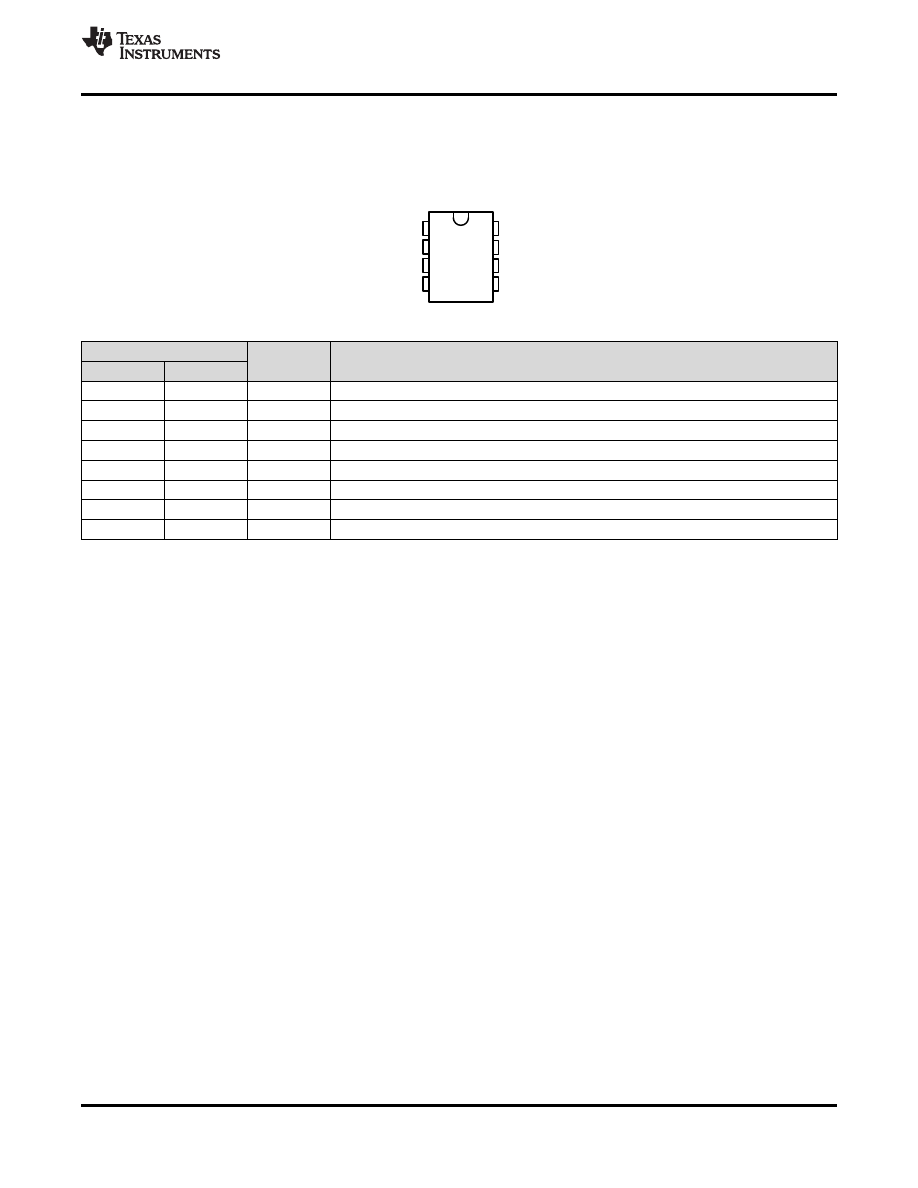
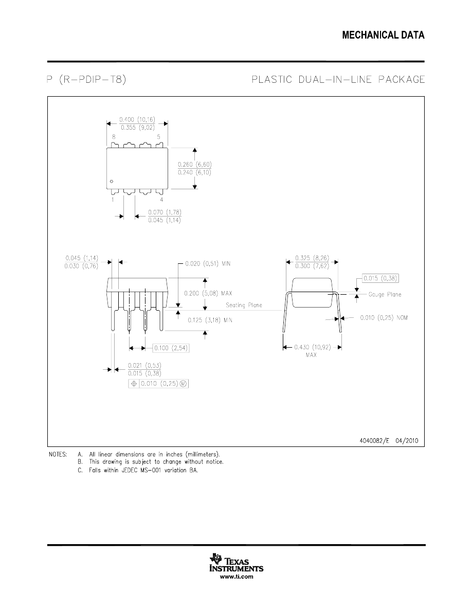
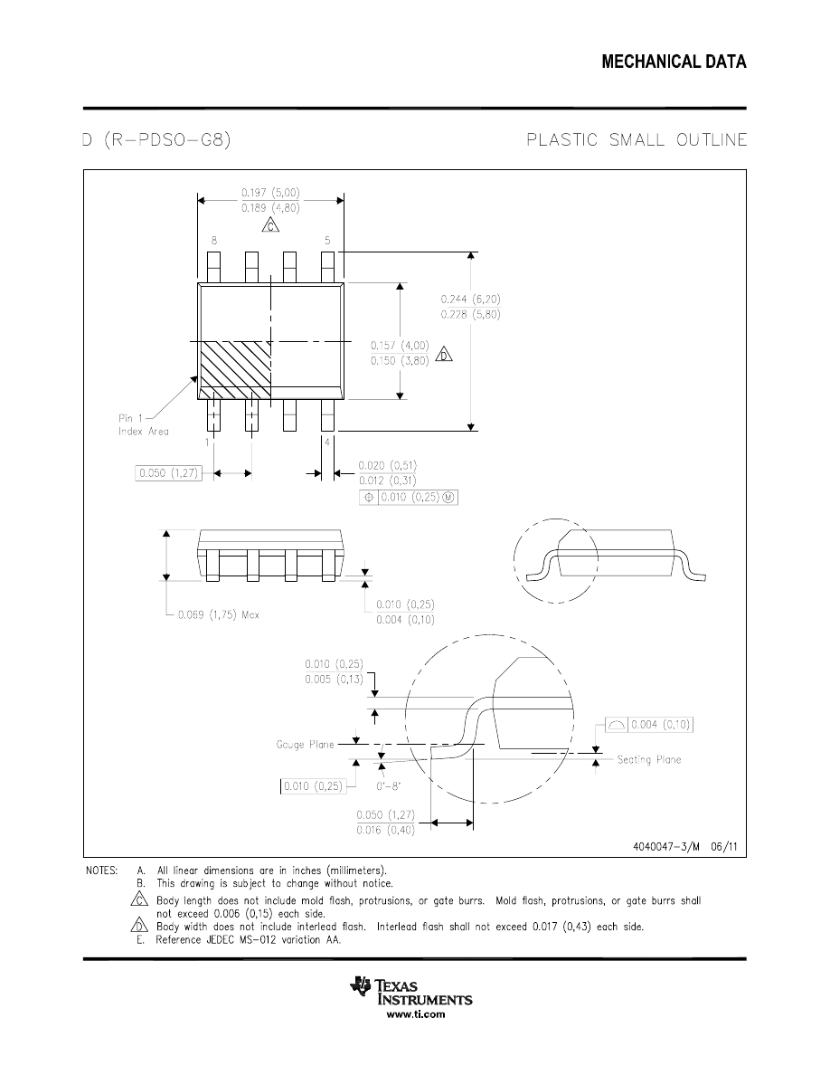
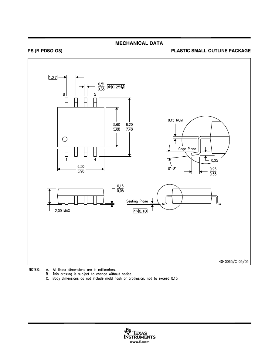
NE5534, SA5534 . . . D (SOIC), P (PDIP),
OR PS (SOP) PACKAGE
NE5534A, SA5534A . . . D (SOIC) OR P (PDIP) PACKAGE
(TOP VIEW)
, , ,
SLOS070D - JULY 1979 - REVISED NOVEMBER 2014
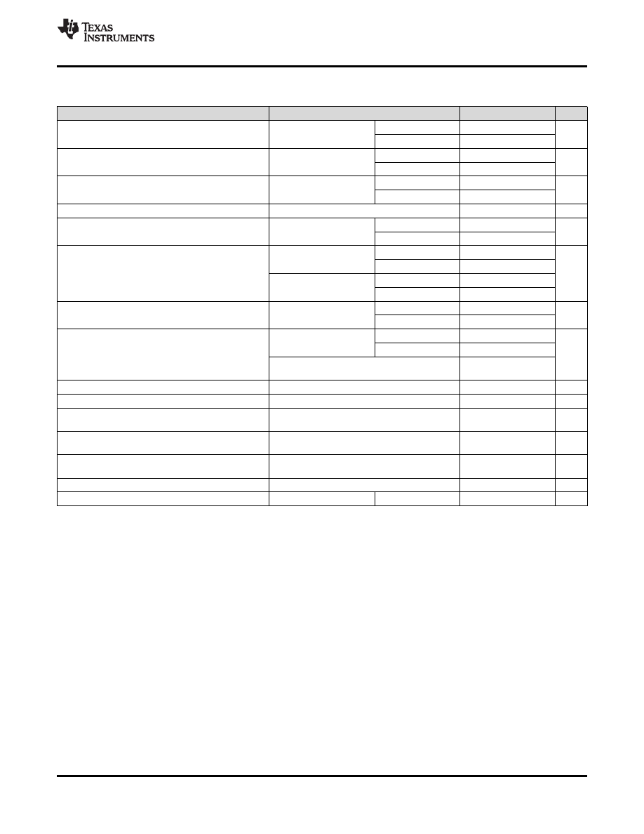
6 Pin Configuration and Functions
Pin Functions
PIN
TYPE
DESCRIPTION
NAME
NO.
BALANCE
1
I
External frequency compensation
COMP/BAL
8
I
External offset voltage adjustment/External frequency compensation
COMP
5
O
External offset voltage adjustment
IN+
3
I
Noninverting input
IN-
2
I
Inverting Input
OUT
6
O
Output
V
CC+
7
Positive Supply
V
CC-
4
Negative Supply
Copyright © 1979-2014, Texas Instruments Incorporated
3
Product Folder Links:

, , ,
SLOS070D - JULY 1979 - REVISED NOVEMBER 2014
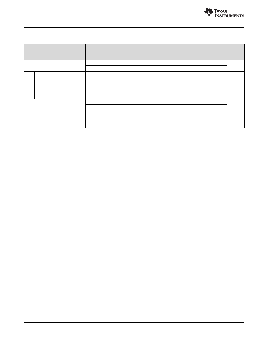
7 Specifications
7.1 Absolute Maximum Ratings
over operating free-air temperature range (unless otherwise noted)
(1)
MIN
TYP
MAX
UNIT
V
CC+
0
22
V
V
CC
Supply voltage
(2)
V
CC-
-22
0
V
Input voltage, either input
(2) (3)
V
CC-
V
CC+
V
Input current
(4)
-10
10
mA
Duration of output short circuit
(5)
Unlimited
T
J
Operating virtual-junction temperature
150
°C
(1)
Stresses beyond those listed under Absolute Maximum Ratings may cause permanent damage to the device. These are stress ratings
only, and functional operation of the device at these or any other conditions beyond those indicated under
is not implied. Exposure to absolute-maximum-rated conditions for extended periods may affect device reliability.
(2)
All voltage values, except differential voltages, are with respect to the midpoint between V
CC+
and V
CC-
.
(3)
The magnitude of the input voltage must never exceed the magnitude of the supply voltage.
(4)
Excessive current will flow if a differential input voltage in excess of approximately 0.6 V is applied between the inputs, unless some
limiting resistance is used.
(5)
The output may be shorted to ground or either power supply. Temperature and/or supply voltages must be limited to ensure the
maximum dissipation rating is not exceeded.
7.2 Handling Ratings
MIN
MAX
UNIT
T
stg
Storage temperature range
-65
150
°C
Human body model (HBM), per ANSI/ESDA/JEDEC JS-001,
0
2000
all pins
V
(ESD)
Electrostatic discharge
V
Charged device model (CDM), per JEDEC specification
0
200
JESD22-C101, all pins
7.3 Recommended Operating Conditions
MIN
MAX
UNIT
V
CC+
5
15
V
V
CC
Supply voltage
V
CC-
-5
-15
V
NE5534, NE5534A
0
70
T
A
Operating free-air temperature
°C
SA5534, SA5534A
-40
85
7.4 Thermal Information
NE5534, NE5534A
SA5534, and SA5534A
THERMAL METRIC
(1)
UNIT
D
P
PS
8 PINS
R
ΘJA
Package thermal impedance
(2) (3)
97
85
95
°C/W
(1)
For more information about traditional and new thermal metrics, see the IC Package Thermal Metrics application report (
).
(2)
The package thermal impedance is calculated in accordance with JESD 51-7.
(3)
Maximum power dissipation is a function of T
J
(max),
Θ
JA
, and T
A
. The maximum allowable power dissipation at any allowable ambient
temperature is P
D
= (T
J
(max) - T
A
) /
Θ
JA.
Operating at the absolute maximum T
J
of 150 °C can affect reliability.
4
Copyright © 1979-2014, Texas Instruments Incorporated
Product Folder Links:
, , ,
SLOS070D - JULY 1979 - REVISED NOVEMBER 2014
7.5 Electrical Characteristics
V
CC ±
= ±15 V, T
A
= 25 °C (unless otherwise noted)
PARAMETER
TEST CONDITIONS
(1)
MIN
TYP
MAX
UNIT
T
A
= 25 °C
0.5
4
V
O
= 0
V
IO
Input offset voltage
mV
R
S
= 50
Ω
T
A
= Full range
5
T
A
= 25 °C
20
300
I
IO
Input offset current
V
O
= 0
nA
T
A
= Full range
400
T
A
= 25 °C
500
1500
I
IB
Input bias current
V
O
= 0
nA
T
A
= Full range
2000
V
ICR
Common-mode input-voltage range
±12
±13
V
V
CC ±
= ±15 V
24
26
V
O(PP)
Maximum peak-to-peak output-voltage swing
R
L
≥ 600 Ω¦
V
V
CC ±
= ±18 V
30
32
T
A
= 25 °C
25
100
V
O
= ±10 V
R
L
≥ 600 Ω¦,
T
A
= Full range
15
A
VD
Large-signal differential-voltage amplification
V/mV
T
A
= 25 °C
25
100
R
L
≥ 2 kΩ¦, V
O
±10 V
T
A
= Full range
15
C
C
= 0
6
A
vd
Small-signal differential-voltage amplification
f = 10 kHz
V/mV
C
C
= 22 pF
2.2
C
C
= 0
200
V
O
= ±10 V
C
C
= 22 pF
95
B
OM
Maximum output-swing bandwidth
kHz
V
CC ±
18 V,
V
O
= ±14 V
70
R
L
= 600
Ω¦
C
C
= 22 pF
B
1
Unity-gain bandwidth
C
C
= 22 pF
C
L
= 100 pF
10
MHz
r
i
Input resistance
30
100
k
Ω¦
A
VD
= 30 dB,
R
L
= 600
Ω¦,
z
o
Output impedance
0.3
Ω¦
C
C
= 22 pF
f = 10 kHz
V
O
= 0,
CMRR Common-mode rejection ratio
V
IC
= V
ICR
min
70
100
dB
R
S
= 50
Ω
V
CC ±
= ±9 V to ±15 V,
k
SVR
Supply-voltage rejection ratio (
ΔV
CC
or
ΔV
IO
)
R
S
= 50
Ω
80
100
dB
V
O
= 0
I
OS
Output short-circuit current
38
mA
I
CC
Total supply current
V
O
= 0, No load
T
A
= 25 °C
4
8
mA
(1)
All characteristics are measured under open-loop conditions with zero common-mode input voltage, unless otherwise specified. For
NE5534 and NE5534A, full range is 0 °C to 70 °C. For SA5534 and SA5534A, full range is -40 °C to 85 °C.
Copyright © 1979-2014, Texas Instruments Incorporated
5
Product Folder Links:
, , ,
SLOS070D - JULY 1979 - REVISED NOVEMBER 2014
7.6 Operating Characteristics
V
CC ±
= ±15 V, T
A
= 25 °C (unless otherwise noted)
NE5534,
NE5534A, SA5534A
SA5534
PARAMETER
TEST CONDITIONS
UNIT
TYP
MIN
TYP
MAX
C
C
= 0
13
13
SR
Slew rate
V/
μs
C
C
= 22 pF
6
6
Rise time
V
I
= 50 mV,
20
20
ns
A
VD
= 1,
R
L
= 600
Ω¦,
C
C
= 22 pF
Overshoot factor
20
20
%
C
L
= 100 pF
t
r
Rise time
V
I
= 50 mV,
50
50
ns
A
VD
= 1,
R
L
= 600
Ω¦,
C
C
= 47 pF
Overshoot factor
35%
35%
C
L
= 500 pF
f = 30 Hz
7
5.5
7
V
n
Equivalent input noise voltage
nV/
√Hz
f = 1 kHz
4
3.5
4.5
f = 30 Hz
2.5
1.5
I
n
Equivalent input noise current
pA/
√Hz
f = 1 kHz
0.6
0.4
F
Average noise figure
R
S
= 5 k
Ω
f = 10Hz to 20 kHz
0.9
dB
6
Copyright © 1979-2014, Texas Instruments Incorporated
Product Folder Links:

A
f - Frequency - Hz
V
CC
±
= ±15 V
T
A
= 25 °C
C
C
= 0 pF
C
C
= 22 pF
10
10
10
10
10
10
6
5
4
3
2
1
VD
-
D
if
fe
re
n
ti
a
l
V
o
lt
a
g
e
A
m
p
li
fi
c
a
ti
o
n
-
V
/m
V
10
100
1 k
10 k
100 k
1 M
10 M 100 M
0.8
0.6
0.5
0.4
0
5
10
N
o
rm
a
li
z
e
d S
le
w R
a
te a
n
d U
n
it
y
-G
a
in B
a
n
d
w
id
th
1
1.1
1.2
15
20
0.9
0.7
| V
CC ±
| - Supply Voltage - V
T
A
= 25 °C
Unity-Gain
Bandwidth
Slew Rate
1
0.8
0.6
0.4
-75 -50
-25
0
25
50
N
o
rm
a
li
z
e
d I
n
p
u
t B
ia
s C
u
rr
e
n
t a
n
d I
n
p
u
t O
ff
s
e
t C
u
rr
e
n
t
1.2
1.4
1.6
75
100
125
T
A
- Free-Air Temperature - °C
V
CC
±
= ±15 V
Offset
Bias
100
1 k
10 k
100 k
1 M
V
f - Frequency - Hz
OPP
-
M
a
x
im
u
m
P
e
a
k
-t
o
-P
e
a
k
O
u
tp
u
t
V
o
lt
a
g
e
-
V
30
25
20
15
10
5
0
V
O(PP)
V
CC
± = ±15 V
T
A
= 25 °C
C
C
= 22 pF
C
C
= 47 pF
C
C
= 0
, , ,
SLOS070D - JULY 1979 - REVISED NOVEMBER 2014
7.7 Typical Characteristics
Figure 1. Normalized Input Bias Current and Input Offset
Figure 2. Maximum Peak-to-Peak Output Voltage
Current
vs Frequency
vs Free-Air Temperature
Figure 3. Large-Signal Differential Voltage Amplification
Figure 4. Normalized Slew Rate and Unity-Gain Bandwidth
vs Frequency
vs Supply Voltage
Figure 6. Total Harmonic Distortion
Figure 5. Normalized Slew Rate and Unity-Gain Bandwidth
vs Frequency
vs Free-Air Temperature
Copyright © 1979-2014, Texas Instruments Incorporated
7
Product Folder Links:

, , ,
SLOS070D - JULY 1979 - REVISED NOVEMBER 2014
Typical Characteristics (continued)
Figure 7. Equivalent Input Noise Voltage
Figure 8. Equivalent Input Noise Current
vs Frequency
vs Frequency
Figure 9. Total Equivalent Input Noise Voltage
vs Source Resistance
8
Copyright © 1979-2014, Texas Instruments Incorporated
Product Folder Links:
V
CC-
OUT
15
Ω¦
15
Ω¦
12 k
Ω¦
12 k
Ω¦
7 pF
12 pF
40 pF
100 pF
IN+
IN-
BALANCE
COMP
COMP/BAL
8
5
7
4
6
2
3
1
V
CC+
, , ,
SLOS070D - JULY 1979 - REVISED NOVEMBER 2014
8 Detailed Description
8.1 Overview
The NE5534, NE5534A, SA5534, and SA5534A devices are high-performance operational amplifiers combining
excellent dc and ac characteristics. Some of the features include very low noise, high output-drive capability, high
unity-gain and maximum-output-swing bandwidths, low distortion, and high slew rate.
These operational amplifiers are compensated internally for a gain equal to or greater than three. Optimization of
the frequency response for various applications can be obtained by use of an external compensation capacitor
between COMP and COMP/BAL. The devices feature input-protection diodes, output short-circuit protection, and
offset-voltage nulling capability with use of the BALANCE and COMP/BAL pins (see the
For the NE5534A and SA5534A devices, a maximum limit is specified for the equivalent input noise voltage.
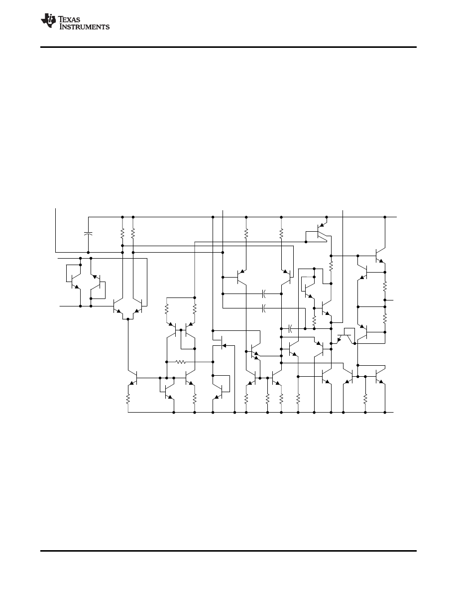
8.2 Functional Block Diagram
Copyright © 1979-2014, Texas Instruments Incorporated
9
Product Folder Links:

, , ,
SLOS070D - JULY 1979 - REVISED NOVEMBER 2014
8.3 Feature Description
8.3.1 Offset-Voltage Null Capability
The input offset voltage of operational amplifiers (op amps) arises from unavoidable mismatches in the
differential input stage of the op-amp circuit caused by mismatched transistor pairs, collector currents, current-
gain betas (
β), collector or emitter resistors, and so on. The input offset pins allow the designer to adjust for
these mismatches by external circuitry. See the
section for more details on
design techniques.
8.3.2 Slew Rate
The slew rate is the rate at which an operational amplifier can change its output when there is a change on the
input. The NE5534 and SA5534 devices have a 13-V/
μs slew rate.
8.3.3 Common-Mode Rejection Ratio
The common-mode rejection ratio (CMRR) of an amplifier is a measure of how well the device rejects unwanted
input signals common to both input leads. It is found by taking the ratio of the change in input offset voltage to
the change in the input voltage and converting to decibels. Ideally the CMRR is infinite, but in practice, amplifiers
are designed to have it as high as possible. The CMRR of the NE5534 and SA5534 devices is 100 dB.
8.3.4 Unity-Gain Bandwidth
The unity-gain bandwidth is the frequency up to which an amplifier with a unity gain may be operated without
greatly distorting the signal. The NE5534 and SA5534 devices have a 10-MHz unity-gain bandwidth.
8.3.5 External Compensation Capability
Frequency compensation with a capacitor may be used to increase the gain-bandwidth product (GBW) of the
amplifier. See the
section for more details on design techniques.
8.4 Device Functional Modes
The NE5534 and SA5534 devices are powered on when the supply is connected. Each of these devices can be
operated as a single supply operational amplifier or dual supply amplifier depending on the application.
10
Copyright © 1979-2014, Texas Instruments Incorporated
Product Folder Links:
-
+
22 k
Ω¦
100 k
Ω¦
V
CC-
V
CC+
C
5534
C
, , ,
SLOS070D - JULY 1979 - REVISED NOVEMBER 2014
9 Application and Implementation
NOTE
Information in the following applications sections is not part of the TI component
specification, and TI does not warrant its accuracy or completeness. TIs customers are
responsible for determining suitability of components for their purposes. Customers should
validate and test their design implementation to confirm system functionality.
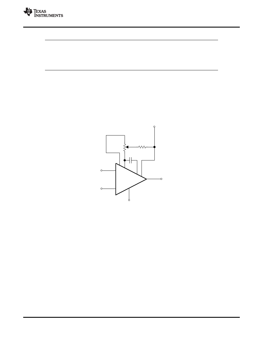
9.1 General Application
The input offset voltage of operational amplifiers (op amps) arises from unavoidable mismatches in the
differential input stage of the op-amp circuit caused by mismatched transistor pairs, collector currents, current-
gain betas (
β), collector or emitter resistors, and so on. The input offset pins allow the designer to adjust for
these mismatches by external circuitry. These input mismatches can be adjusted by putting resistors or a
potentiometer between the inputs as shown in
. A potentiometer can be used to fine tune the circuit
during testing or for applications which require precision offset control. More information about designing using
the input-offset pins, see Offset Voltage of Operational Amplifiers
).
Frequency Compensation and Offset-Voltage Nulling Circuit
Figure 10. Application Circuit
Copyright © 1979-2014, Texas Instruments Incorporated
11
Product Folder Links:
12 V
+
V
IN
V
OUT
10 k
, , ,
SLOS070D - JULY 1979 - REVISED NOVEMBER 2014
9.2 Typical Application
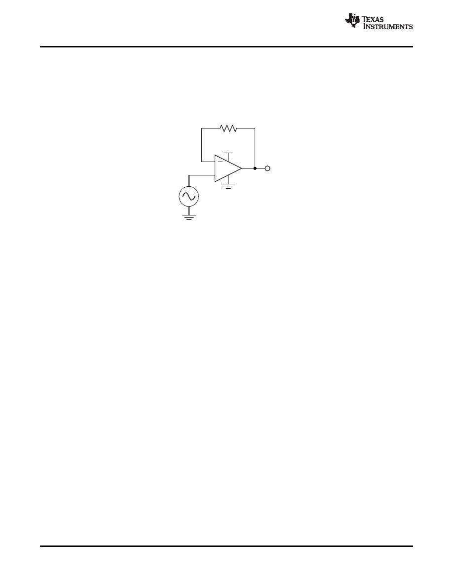
The voltage follower configuration of the operational amplifier is used for applications where a weak signal is
used to drive a relatively high current load. This circuit is also called a buffer amplifier or unity gain amplifier. The
inputs of an operational amplifier have a very high resistance which puts a negligible current load on the voltage
source. The output resistance of the operational amplifier is almost negligible, so it can provide as much current
as necessary to the output load.
Figure 11. Voltage Follower Schematic
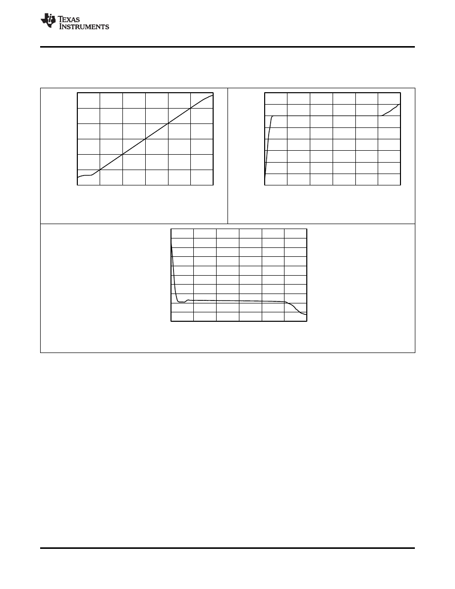
9.2.1 Design Requirements
Output range of 2 V to 11 V
Input range of 2 V to 11 V
9.2.2 Detailed Design Procedure
9.2.2.1 Output Voltage Swing
The output voltage of an operational amplifier is limited by its internal circuitry to some level below the supply
rails. For this amplifier, the output voltage swing is within ±12 V, which accommodates the input and output
voltage requirements.
9.2.2.2 Supply and Input Voltage
For correct operation of the amplifier, neither input must be higher than the recommended positive supply rail
voltage or lower than the recommended negative supply rail voltage. The chosen amplifier must be able to
operate at the supply voltage that accommodates the inputs. Because the input for this application goes up to
11 V, the supply voltage must be 12 V. Using a negative voltage on the lower rail rather than ground, allows the
amplifier to maintain linearity for inputs below 2 V.
12
Copyright © 1979-2014, Texas Instruments Incorporated
Product Folder Links:
0
2
4
6
8
10
12
14
16
18
20
0
2
4
6
8
10
12
ICC
(
m
A
)
VIN (V)
C003
0
2
4
6
8
10
12
0
2
4
6
8
10
12
V
OUT
(
V
)
VIN (V)
C001
±
12
±
10
±
8
±
6
±
4
±
2
0
2
4
0
2
4
6
8
10
12
II
N
(m
A
)
VIN (V)
C002
, , ,
SLOS070D - JULY 1979 - REVISED NOVEMBER 2014
Typical Application (continued)
9.2.3 Application Curves for Output Characteristics
Figure 12. Output Voltage vs Input Voltage
Figure 13. Current Drawn by the Input of the Voltage
Follower (I
IN
) vs the Input Voltage
Figure 14. Current Drawn from Supply (I
CC
) vs the Input Voltage
Copyright © 1979-2014, Texas Instruments Incorporated
13
Product Folder Links:

, , ,
SLOS070D - JULY 1979 - REVISED NOVEMBER 2014
10 Power Supply Recommendations
The NE5534 and SA5534 devices are specified for operation from ±5 to ±15 V; many specifications apply from
0 °C to 70 °C for the NE5534 device and -40 °C to 85 °C for the SA5534 device.
CAUTION
Supply voltages larger than ±22 V can permanently damage the device (see the
).
Place 0.1-
μF bypass capacitors close to the power-supply pins to reduce errors coupling in from noisy or high
impedance power supplies. For more detailed information on bypass capacitor placement, refer to the
14
Copyright © 1979-2014, Texas Instruments Incorporated
Product Folder Links:

BALANCE
VCC+
IN1
Ã
IN1+
VCC
Ã
COMP/BAL
OUT
COMP
RG
RIN
RF
GND
VIN
VS-
GND
VS+
GND
Run the input traces as far
away from the supply lines
as possible
Only needed for
dual-supply
operation
Place components close to
device and to each other to
reduce parasitic errors
Use low-ESR, ceramic
bypass capacitor
(or GND for single supply)
Ground (GND) plane on another layer
VOUT
+
RIN
RG
RF
VOUT
VIN
, , ,
SLOS070D - JULY 1979 - REVISED NOVEMBER 2014
11 Layout
11.1 Layout Guidelines
For best operational performance of the device, use good PCB layout practices, including:
Noise can propagate into analog circuitry through the power pins of the circuit as a whole, as well as the
operational amplifier. Bypass capacitors are used to reduce the coupled noise by providing low-impedance
power sources local to the analog circuitry.
-
Connect low-ESR, 0.1-
μF ceramic bypass capacitors between each supply pin and ground, placed as
close to the device as possible. A single bypass capacitor from V+ to ground is applicable for single
supply applications.
Separate grounding for analog and digital portions of circuitry is one of the simplest and most-effective
methods of noise suppression. On multilayer PCBs, one or more layers are usually devoted to ground planes.
A ground plane helps distribute heat and reduces EMI noise pickup. Make sure to physically separate digital
and analog grounds, paying attention to the flow of the ground current. For more detailed information, refer to
Circuit Board Layout Techniques (
To reduce parasitic coupling, run the input traces as far away from the supply or output traces as possible. If
it is not possible to keep them separate, it is much better to cross the sensitive trace perpendicularly, as
opposed to in parallel, with the noisy trace.
Place the external components as close to the device as possible. Keeping RF and RG close to the inverting
input minimizes parasitic capacitance, as shown in .
Keep the length of input traces as short as possible. Always remember that the input traces are the most
sensitive part of the circuit.
Consider a driven, low-impedance guard ring around the critical traces. A guard ring can significantly reduce
leakage currents from nearby traces that are at different potentials.
11.2 Layout Example
Figure 15. Operational Amplifier Schematic for Noninverting Configuration
Figure 16. Operational Amplifier Board Layout for Noninverting Configuration
Copyright © 1979-2014, Texas Instruments Incorporated
15
Product Folder Links:

, , ,
SLOS070D - JULY 1979 - REVISED NOVEMBER 2014
12 Device and Documentation Support
12.1 Related Links
The table below lists quick access links. Categories include technical documents, support and community
resources, tools and software, and quick access to sample or buy.
Table 1. Related Links
TECHNICAL
TOOLS &
SUPPORT &
PARTS
PRODUCT FOLDER
SAMPLE & BUY
DOCUMENTS
SOFTWARE
COMMUNITY
NE5534
NE5534A
SA5534
SA5534A
12.2 Trademarks
All trademarks are the property of their respective owners.
12.3 Electrostatic Discharge Caution
These devices have limited built-in ESD protection. The leads should be shorted together or the device placed in conductive foam
during storage or handling to prevent electrostatic damage to the MOS gates.
12.4 Glossary
TI Glossary.
This glossary lists and explains terms, acronyms, and definitions.
13 Mechanical, Packaging, and Orderable Information
The following pages include mechanical, packaging, and orderable information. This information is the most
current data available for the designated devices. This data is subject to change without notice and revision of
this document. For browser-based versions of this data sheet, refer to the left-hand navigation.
16
Copyright © 1979-2014, Texas Instruments Incorporated
Product Folder Links:

PACKAGE OPTION ADDENDUM
www.ti.com
24-Apr-2015
Addendum-Page 1
PACKAGING INFORMATION
Orderable Device
Status
(1)
Package Type Package
Drawing
Pins Package
Qty
Eco Plan
(2)
Lead/Ball Finish
(6)
MSL Peak Temp
(3)
Op Temp ( °C)
Device Marking
(4/5)
Samples
NE5534AD
ACTIVE
SOIC
D
8
75
Green (RoHS
& no Sb/Br)
CU NIPDAU
Level-2-260C-1 YEAR
0 to 70
5534A
NE5534ADR
ACTIVE
SOIC
D
8
2500
Green (RoHS
& no Sb/Br)
CU NIPDAU
Level-2-260C-1 YEAR
0 to 70
5534A
NE5534ADRE4
ACTIVE
SOIC
D
8
2500
Green (RoHS
& no Sb/Br)
CU NIPDAU
Level-2-260C-1 YEAR
0 to 70
5534A
NE5534ADRG4
ACTIVE
SOIC
D
8
2500
Green (RoHS
& no Sb/Br)
CU NIPDAU
Level-2-260C-1 YEAR
0 to 70
5534A
NE5534AJG
OBSOLETE
CDIP
JG
8
TBD
Call TI
Call TI
-55 to 125
NE5534AP
ACTIVE
PDIP
P
8
50
Pb-Free
(RoHS)
CU NIPDAU
N / A for Pkg Type
0 to 70
NE5534AP
NE5534APE4
ACTIVE
PDIP
P
8
50
Pb-Free
(RoHS)
CU NIPDAU
N / A for Pkg Type
0 to 70
NE5534AP
NE5534D
ACTIVE
SOIC
D
8
75
Green (RoHS
& no Sb/Br)
CU NIPDAU
Level-2-260C-1 YEAR
0 to 70
NE5534
NE5534DR
ACTIVE
SOIC
D
8
2500
Green (RoHS
& no Sb/Br)
CU NIPDAU
Level-2-260C-1 YEAR
0 to 70
NE5534
NE5534DRE4
ACTIVE
SOIC
D
8
2500
Green (RoHS
& no Sb/Br)
CU NIPDAU
Level-2-260C-1 YEAR
0 to 70
NE5534
NE5534DRG4
ACTIVE
SOIC
D
8
2500
Green (RoHS
& no Sb/Br)
CU NIPDAU
Level-2-260C-1 YEAR
0 to 70
NE5534
NE5534IP
OBSOLETE
PDIP
P
8
TBD
Call TI
Call TI
0 to 70
NE5534P
ACTIVE
PDIP
P
8
50
Pb-Free
(RoHS)
CU NIPDAU
N / A for Pkg Type
0 to 70
NE5534P
NE5534PE4
ACTIVE
PDIP
P
8
50
Pb-Free
(RoHS)
CU NIPDAU
N / A for Pkg Type
0 to 70
NE5534P
SA5534AD
ACTIVE
SOIC
D
8
75
Green (RoHS
& no Sb/Br)
CU NIPDAU
Level-2-260C-1 YEAR
-40 to 85
SA5534A
SA5534ADG4
ACTIVE
SOIC
D
8
75
Green (RoHS
& no Sb/Br)
CU NIPDAU
Level-2-260C-1 YEAR
-40 to 85
SA5534A
SA5534ADR
ACTIVE
SOIC
D
8
2500
Green (RoHS
& no Sb/Br)
CU NIPDAU
Level-2-260C-1 YEAR
-40 to 85
SA5534A
SA5534AP
ACTIVE
PDIP
P
8
50
Pb-Free
(RoHS)
CU NIPDAU
N / A for Pkg Type
-40 to 85
SA5534AP
PACKAGE OPTION ADDENDUM
www.ti.com
24-Apr-2015
Addendum-Page 2
Orderable Device
Status
(1)
Package Type Package
Drawing
Pins Package
Qty
Eco Plan
(2)
Lead/Ball Finish
(6)
MSL Peak Temp
(3)
Op Temp ( °C)
Device Marking
(4/5)
Samples
SA5534APE4
ACTIVE
PDIP
P
8
50
Pb-Free
(RoHS)
CU NIPDAU
N / A for Pkg Type
-40 to 85
SA5534AP
SA5534D
ACTIVE
SOIC
D
8
75
Green (RoHS
& no Sb/Br)
CU NIPDAU
Level-2-260C-1 YEAR
-40 to 85
SA5534
SA5534DE4
ACTIVE
SOIC
D
8
75
Green (RoHS
& no Sb/Br)
CU NIPDAU
Level-2-260C-1 YEAR
-40 to 85
SA5534
SA5534DR
ACTIVE
SOIC
D
8
2500
Green (RoHS
& no Sb/Br)
CU NIPDAU
Level-2-260C-1 YEAR
-40 to 85
SA5534
SA5534P
ACTIVE
PDIP
P
8
50
Pb-Free
(RoHS)
CU NIPDAU
N / A for Pkg Type
-40 to 85
SA5534P
SA5534PSR
ACTIVE
SO
PS
8
2000
Green (RoHS
& no Sb/Br)
CU NIPDAU
Level-1-260C-UNLIM
-40 to 85
SA5534
(1)
The marketing status values are defined as follows:
ACTIVE: Product device recommended for new designs.
LIFEBUY: TI has announced that the device will be discontinued, and a lifetime-buy period is in effect.
NRND: Not recommended for new designs. Device is in production to support existing customers, but TI does not recommend using this part in a new design.
PREVIEW: Device has been announced but is not in production. Samples may or may not be available.
OBSOLETE: TI has discontinued the production of the device.
(2)
Eco Plan - The planned eco-friendly classification: Pb-Free (RoHS), Pb-Free (RoHS Exempt), or Green (RoHS & no Sb/Br) - please check
for the latest availability
information and additional product content details.
TBD: The Pb-Free/Green conversion plan has not been defined.
Pb-Free (RoHS): TI's terms "Lead-Free" or "Pb-Free" mean semiconductor products that are compatible with the current RoHS requirements for all 6 substances, including the requirement that
lead not exceed 0.1% by weight in homogeneous materials. Where designed to be soldered at high temperatures, TI Pb-Free products are suitable for use in specified lead-free processes.
Pb-Free (RoHS Exempt): This component has a RoHS exemption for either 1) lead-based flip-chip solder bumps used between the die and package, or 2) lead-based die adhesive used between
the die and leadframe. The component is otherwise considered Pb-Free (RoHS compatible) as defined above.
Green (RoHS & no Sb/Br): TI defines "Green" to mean Pb-Free (RoHS compatible), and free of Bromine (Br) and Antimony (Sb) based flame retardants (Br or Sb do not exceed 0.1% by weight
in homogeneous material)
(3)
MSL, Peak Temp. - The Moisture Sensitivity Level rating according to the JEDEC industry standard classifications, and peak solder temperature.
(4)
There may be additional marking, which relates to the logo, the lot trace code information, or the environmental category on the device.
(5)
Multiple Device Markings will be inside parentheses. Only one Device Marking contained in parentheses and separated by a "~" will appear on a device. If a line is indented then it is a continuation
of the previous line and the two combined represent the entire Device Marking for that device.
PACKAGE OPTION ADDENDUM
www.ti.com
24-Apr-2015
Addendum-Page 3
(6)
Lead/Ball Finish - Orderable Devices may have multiple material finish options. Finish options are separated by a vertical ruled line. Lead/Ball Finish values may wrap to two lines if the finish
value exceeds the maximum column width.
Important Information and Disclaimer:The information provided on this page represents TI's knowledge and belief as of the date that it is provided. TI bases its knowledge and belief on information
provided by third parties, and makes no representation or warranty as to the accuracy of such information. Efforts are underway to better integrate information from third parties. TI has taken and
continues to take reasonable steps to provide representative and accurate information but may not have conducted destructive testing or chemical analysis on incoming materials and chemicals.
TI and TI suppliers consider certain information to be proprietary, and thus CAS numbers and other limited information may not be available for release.
In no event shall TI's liability arising out of such information exceed the total purchase price of the TI part(s) at issue in this document sold by TI to Customer on an annual basis.
TAPE AND REEL INFORMATION
*All dimensions are nominal
Device
Package
Type
Package
Drawing
Pins
SPQ
Reel
Diameter
(mm)
Reel
Width
W1 (mm)
A0
(mm)
B0
(mm)
K0
(mm)
P1
(mm)
W
(mm)
Pin1
Quadrant
NE5534ADR
SOIC
D
8
2500
330.0
12.4
6.4
5.2
2.1
8.0
12.0
Q1
NE5534DR
SOIC
D
8
2500
330.0
12.4
6.4
5.2
2.1
8.0
12.0
Q1
SA5534ADR
SOIC
D
8
2500
330.0
12.4
6.4
5.2
2.1
8.0
12.0
Q1
SA5534DR
SOIC
D
8
2500
330.0
12.4
6.4
5.2
2.1
8.0
12.0
Q1
SA5534PSR
SO
PS
8
2000
330.0
16.4
8.2
6.6
2.5
12.0
16.0
Q1
PACKAGE MATERIALS INFORMATION
www.ti.com
1-Oct-2014
Pack Materials-Page 1
*All dimensions are nominal
Device
Package Type
Package Drawing
Pins
SPQ
Length (mm)
Width (mm)
Height (mm)
NE5534ADR
SOIC
D
8
2500
340.5
338.1
20.6
NE5534DR
SOIC
D
8
2500
340.5
338.1
20.6
SA5534ADR
SOIC
D
8
2500
340.5
338.1
20.6
SA5534DR
SOIC
D
8
2500
340.5
338.1
20.6
SA5534PSR
SO
PS
8
2000
367.0
367.0
38.0
PACKAGE MATERIALS INFORMATION
www.ti.com
1-Oct-2014
Pack Materials-Page 2
MECHANICAL DATA
MCER001A - JANUARY 1995 - REVISED JANUARY 1997
POST OFFICE BOX 655303
DALLAS, TEXAS 75265
JG (R-GDIP-T8)
CERAMIC DUAL-IN-LINE
0.310 (7,87)
0.290 (7,37)
0.014 (0,36)
0.008 (0,20)
Seating Plane
4040107/C 08/96
5
4
0.065 (1,65)
0.045 (1,14)
8
1
0.020 (0,51) MIN
0.400 (10,16)
0.355 (9,00)
0.015 (0,38)
0.023 (0,58)
0.063 (1,60)
0.015 (0,38)
0.200 (5,08) MAX
0.130 (3,30) MIN
0.245 (6,22)
0.280 (7,11)
0.100 (2,54)
0
°
-15
°
NOTES: A. All linear dimensions are in inches (millimeters).
B. This drawing is subject to change without notice.
C. This package can be hermetically sealed with a ceramic lid using glass frit.
D. Index point is provided on cap for terminal identification.
E. Falls within MIL STD 1835 GDIP1-T8


IMPORTANT NOTICE
Texas Instruments Incorporated and its subsidiaries (TI) reserve the right to make corrections, enhancements, improvements and other
changes to its semiconductor products and services per JESD46, latest issue, and to discontinue any product or service per JESD48, latest
issue. Buyers should obtain the latest relevant information before placing orders and should verify that such information is current and
complete. All semiconductor products (also referred to herein as components) are sold subject to TIs terms and conditions of sale
supplied at the time of order acknowledgment.
TI warrants performance of its components to the specifications applicable at the time of sale, in accordance with the warranty in TIs terms
and conditions of sale of semiconductor products. Testing and other quality control techniques are used to the extent TI deems necessary
to support this warranty. Except where mandated by applicable law, testing of all parameters of each component is not necessarily
performed.
TI assumes no liability for applications assistance or the design of Buyers products. Buyers are responsible for their products and
applications using TI components. To minimize the risks associated with Buyers products and applications, Buyers should provide
adequate design and operating safeguards.
TI does not warrant or represent that any license, either express or implied, is granted under any patent right, copyright, mask work right, or
other intellectual property right relating to any combination, machine, or process in which TI components or services are used. Information
published by TI regarding third-party products or services does not constitute a license to use such products or services or a warranty or
endorsement thereof. Use of such information may require a license from a third party under the patents or other intellectual property of the
third party, or a license from TI under the patents or other intellectual property of TI.
Reproduction of significant portions of TI information in TI data books or data sheets is permissible only if reproduction is without alteration
and is accompanied by all associated warranties, conditions, limitations, and notices. TI is not responsible or liable for such altered
documentation. Information of third parties may be subject to additional restrictions.
Resale of TI components or services with statements different from or beyond the parameters stated by TI for that component or service
voids all express and any implied warranties for the associated TI component or service and is an unfair and deceptive business practice.
TI is not responsible or liable for any such statements.
Buyer acknowledges and agrees that it is solely responsible for compliance with all legal, regulatory and safety-related requirements
concerning its products, and any use of TI components in its applications, notwithstanding any applications-related information or support
that may be provided by TI. Buyer represents and agrees that it has all the necessary expertise to create and implement safeguards which
anticipate dangerous consequences of failures, monitor failures and their consequences, lessen the likelihood of failures that might cause
harm and take appropriate remedial actions. Buyer will fully indemnify TI and its representatives against any damages arising out of the use
of any TI components in safety-critical applications.
In some cases, TI components may be promoted specifically to facilitate safety-related applications. With such components, TIs goal is to
help enable customers to design and create their own end-product solutions that meet applicable functional safety standards and
requirements. Nonetheless, such components are subject to these terms.
No TI components are authorized for use in FDA Class III (or similar life-critical medical equipment) unless authorized officers of the parties
have executed a special agreement specifically governing such use.
Only those TI components which TI has specifically designated as military grade or enhanced plastic are designed and intended for use in
military/aerospace applications or environments. Buyer acknowledges and agrees that any military or aerospace use of TI components
which have not been so designated is solely at the Buyer's risk, and that Buyer is solely responsible for compliance with all legal and
regulatory requirements in connection with such use.
TI has specifically designated certain components as meeting ISO/TS16949 requirements, mainly for automotive use. In any case of use of
non-designated products, TI will not be responsible for any failure to meet ISO/TS16949.
Products
Applications
Audio
Automotive and Transportation
Amplifiers
Communications and Telecom
Data Converters
Computers and Peripherals
DLP ® Products
Consumer Electronics
DSP
Energy and Lighting
Clocks and Timers
Industrial
Interface
Medical
Logic
Security
Power Mgmt
Space, Avionics and Defense
Microcontrollers
Video and Imaging
RFID
OMAP Applications Processors
TI E2E Community
Wireless Connectivity
Mailing Address: Texas Instruments, Post Office Box 655303, Dallas, Texas 75265
Copyright © 2015, Texas Instruments Incorporated
Document Outline

