| Secciones |
|---|
| Foros Electrónica |
|
|
| Boletines de correo |
 |
DATA SHEET
Product specification
Supersedes data of January 1994
File under Integrated Circuits, IC01
1997 Feb 24
INTEGRATED CIRCUITS
SAA6579
Radio Data System (RDS)
demodulator
1997 Feb 24
2
Philips Semiconductors
Product specification
Radio Data System (RDS) demodulator
SAA6579
FEATURES
Anti-aliasing filter (2nd order)
Integrated 57 kHz band-pass filter (8th order)
Reconstruction filter (2nd order)
Clocked comparator with automatic offset compensation
57 kHz carrier regeneration
Synchronous demodulator for 57 kHz modulated RDS
signals
Selectable 4.332/8.664 MHz crystal oscillator with
variable dividers
Clock regeneration with lock on biphase data rate
Biphase symbol decoder with integrate and dump
functions
Differential decoder
Signal quality detector
Subcarrier output.
GENERAL DESCRIPTION
The integrated CMOS circuit SAA6579 is an RDS
demodulator. It recovers the additional inaudible RDS
information which is transmitted by FM radio broadcasting.
The data signal RDDA and the clock signal RDCL are
provided as outputs for further processing by a suitable
decoder (microcomputer).
The operational functions of the device are in accordance
with the
CENELEC EN 50067.
QUICK REFERENCE DATA
ORDERING INFORMATION
SYMBOL
PARAMETER
MIN.
TYP.
MAX.
UNIT
V
DDA
analog supply voltage (pin 5)
3.6
5.0
5.5
V
V
DDD
digital supply voltage (pin 12)
3.6
5.0
5.5
V
I
tot
total supply current
-
6
-
mA
V
i(rms)
RDS input amplitude (RMS value; pin 4)
1
-
-
mV
V
OH
HIGH level output voltage for signals RDDA, RDCL, QUAL and T57
4.4
-
-
V
V
OL
LOW level output voltage for signals RDDA, RDCL, QUAL and T57
-
-
0.4
V
T
amb
operating ambient temperature
-
40
-
+85
°
C
TYPE
NUMBER
PACKAGE
NAME
DESCRIPTION
VERSION
SAA6579
DIP16
plastic dual in-line package; 16 leads (300 mil); long body
SOT38-1
SAA6579T
SO16
plastic small outline package; 16 leads; body width 7.5 mm
SOT162-1
1997 Feb 24
3
Philips Semiconductors
Product specification
Radio Data System (RDS) demodulator
SAA6579
BLOCK DIAGRAM
Fig.1 Block diagram and application circuit.
Via pin MODE two different crystal frequencies can be used.
MODE
CRYSTAL CLOCK
LOW
4.332 MHz
HIGH
8.664 MHz
handbook, full pagewidth
SAA6579
0.1
µ
F
ANTI-
ALIASING
FILTER
57 kHz
BANDPASS
(8th ORDER)
RECONSTRUCTION
FILTER
OSCILLATOR
AND
DIVIDER
CLOCKED
COMPARATOR
COSTAS LOOP
VARIABLE AND
FIXED DIVIDER
CLOCK
REGENERATION
AND SYNC
BIPHASE
SYMBOL
DECODER
DIFFERENTIAL
DECODER
TEST LOGIC AND OUTPUT
SELECTOR SWITCH
REFERENCE
VOLTAGE
2.2
µ
F
4
7
8
5
3
6
VDDA
Vref
V
P1
13
14
QUAL
RDDA
RDCL
T57
QUALITY BIT
GENERATOR
1
2
15
16
11
12
2.2 k
Ω¦
82 pF
47 pF
4.332/8.664 MHz
MPX
signal
330 pF
9
10
MODE
TEST
560 pF
MEH162
VSSD
V
DDD
+
5 V
+5 V
OSCO
OSCI
MUX
SCOUT
CIN
0.1
µ
F
VSSA
1997 Feb 24
4
Philips Semiconductors
Product specification
Radio Data System (RDS) demodulator
SAA6579
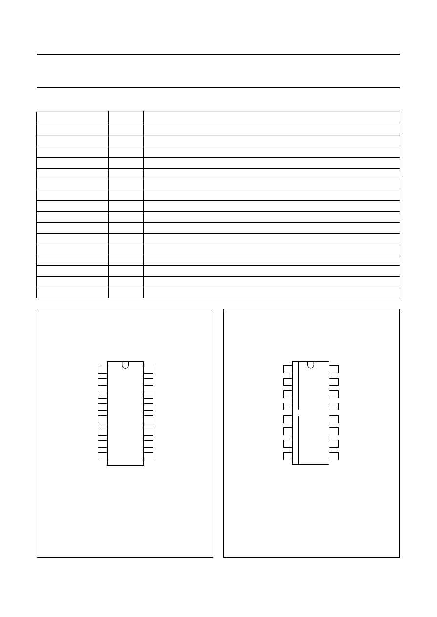
PINNING
SYMBOL
PIN
DESCRIPTION
QUAL
1
quality indication output
RDDA
2
RDS data output
V
ref
3
reference voltage output (0.5V
DDA
)
MUX
4
multiplex signal input
V
DDA
5
+5 V supply voltage for analog part
V
SSA
6
ground for analog part (0 V)
CIN
7
subcarrier input to comparator
SCOUT
8
subcarrier output of reconstruction filter
MODE
9
oscillator mode/test control input
TEST
10
test enable input
V
SSD
11
ground for digital part (0 V)
V
DDD
12
+5 V supply voltage for digital part
OSCI
13
oscillator input
OSCO
14
oscillator output
T57
15
57 kHz clock signal output
RDCL
16
RDS clock output
handbook, halfpage
SAA6579
MGD684
1
2
3
4
5
6
7
8
QUAL
RDDA
Vref
MUX
VDDA
VSSA
CIN
SCOUT
RDCL
T57
OSCO
OSCI
VDDD
VSSD
TEST
MODE
16
15
14
13
12
11
10
9
Fig.2 Pin configuration.
Fig.3 Pin configuration.
handbook, halfpage
MGD685
1
2
3
4
5
6
7
8
16
15
14
13
12
11
10
9
QUAL
RDDA
Vref
MUX
VDDA
VSSA
CIN
SCOUT
RDCL
T57
OSCO
OSCI
VDDD
VSSD
TEST
MODE
SAA6579T
1997 Feb 24
5
Philips Semiconductors
Product specification
Radio Data System (RDS) demodulator
SAA6579
LIMITING VALUES
In accordance with the Absolute Maximum Rating System (IEC 134); ground pins 6 and 11 connected together.
Notes
1. Equivalent to discharging a 200 pF capacitor via a 0
Ω¦
series resistor.
2. Equivalent to discharging a 100 pF capacitor via a 1.5 k
Ω¦
series resistor.
SYMBOL
PARAMETER
CONDITIONS
MIN.
MAX.
UNIT
V
DDA
analog supply voltage (pin 5)
0
6
V
V
DDD
digital supply voltage (pin 12)
0
6
V
V
n
voltage on all pins; grounds excluded
-
0.5
V
DDX
+ 0.5
V
T
stg
storage temperature
-
40
+150
°
C
T
amb
operating ambient temperature
-
40
+85
°
C
V
es
electrostatic handling for all pins except
pins 9 and 10
note 1
±
300
-
V
note 2
+1500
-
3000
V
FUNCTIONAL DESCRIPTION
The SAA6579 is a demodulator circuit for RDS
applications. It contains a 57 kHz bandpass filter and a
digital demodulator to regenerate the RDS data stream out
of the multiplex signal (MPX).
Filter part
The MUX signal is band-limited by a second-order
anti-aliasing-filter and fed through a 57 kHz band-pass
filter (8th order band-pass filter with 3 kHz bandwidth) to
separate the RDS signals. This filter uses switched
capacitor technique and is clocked by a clock frequency of
541.5 kHz derived from the 4.332/8.664 MHz crystal
oscillator. Then the signal is fed to the reconstruction filter
to smooth the sampled and filtered RDS signal before it is
output on pin 8. The signal is AC-coupled to the
comparator (pin 7). The comparator is clocked with a
frequency of 228 kHz (synchronized by the 57 kHz of the
demodulator).
Digital part
The synchronous demodulator (Costas loop circuit) with
carrier regeneration demodulates the internal coupled,
digitized signal. The suppressed carrier is recovered from
the two sidebands (Costas loop). The demodulated signal
is low-pass-filtered in such a way that the overall pulse
shape (transmitter and receiver) approaches a
cosinusoidal form in conjunction with the following
Integrate and dump circuit.
The data-spectrum shaping is split into two equal parts and
handled in the transmitter and in the receiver. Ideally, the
data filtering should be equal in both of these parts.
The overall data-channel-spectrum shaping of the
transmitter and the receiver is approximately 100% roll-off.
The Integrate and dump circuit performs an integration
over a clock period. This results in a demodulated and
valid RDS signal in form of biphase symbols being output
from the integrate and dump circuit. The final stages of
RDS data processing are the biphase symbol decoding
and the differential decoding. After synchronization by
data clock RDCL (pin 16) data appears on the RDDA
output (pin 2). The output of the biphase symbol decoder
is evaluated by a special circuit to provide an indication of
good data (QUAL = HIGH) or corrupt data (QUAL = LOW).
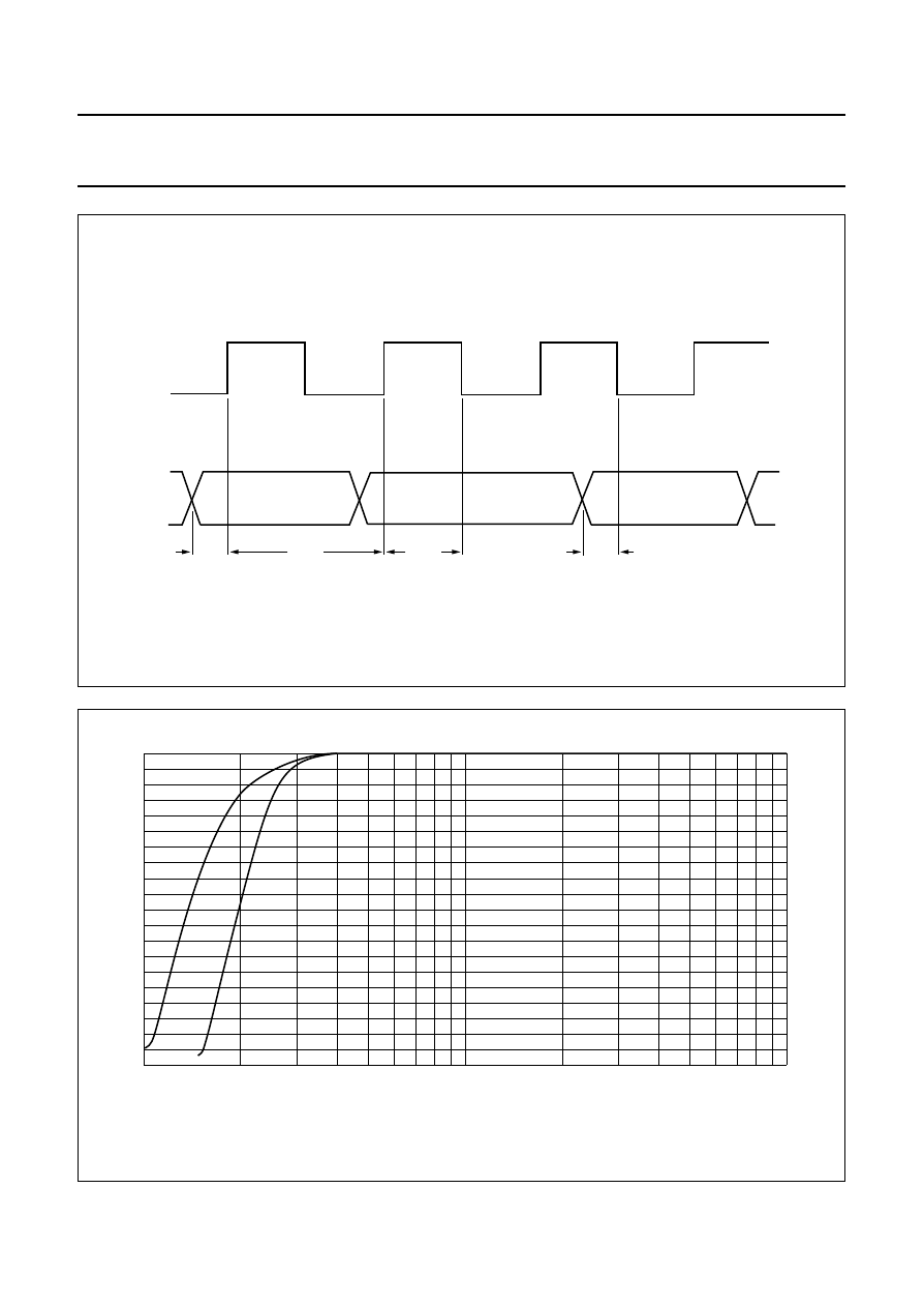
Timing
Fixed and variable dividers are applied to the
4.332/8.664 MHz crystal oscillator to generate the
1.1875 kHz RDS clock RDCL, which is synchronized by
the incoming data. Which ever clock edge is considered
(positive or negative going edge) the data will remain valid
for 399
µ
s after the clock transition. The timing of data
change is 4
µ
s before a clock change. Which clock
transition (positive or negative going clock) the data
change occurs in, depends on the lock conditions and is
arbitrary (bit slip).
During poor reception it is possible that faults in phase
occur, then the clock signal stays uninterrupted, and data
is constant for 1.5 clock periods. Normally, faults in phase
do not occur on a cyclic basis. If however, faults in phase
occur in this way, the minimum spacing between two
possible faults in phase depends on the data being
transmitted. The minimum spacing cannot be less than
16 clock periods. The quality bit changes only at the time
of a data change.
1997 Feb 24
6
Philips Semiconductors
Product specification
Radio Data System (RDS) demodulator
SAA6579
CHARACTERISTICS
V
DDA
= V
DDD
= 5 V; T
amb
= 25
°
C and measurements taken in Fig.1; unless otherwise specified.
SYMBOL
PARAMETER
CONDITIONS
MIN.
TYP.
MAX.
UNIT
V
DDA
analog supply voltage (pin 5)
3.6
5.0
5.5
V
V
DDD
digital supply voltage (pin 12)
3.6
5.0
5.5
V
I
tot
total supply current
I
5
+ I
12
-
6
-
mA
V
ref
reference voltage (pin 3)
V
DDA
= 5 V
-
2.5
-
V
MPX input (signal before the capacitor on pin 4)
V
i MPX(rms)
RDS amplitude (RMS value)
∆
f =
±
1.2 kHz RDS;
∆
f =
±
3.5 kHz ARI; see Fig.5
1
-
-
mV
V
i MPX(p-p)
maximum input signal capability
(peak-to-peak value)
f = 57
±
2 kHz
200
-
-
mV
f < 50 kHz
1.4
-
-
V
f < 15 kHz
2.8
-
-
V
f > 70 kHz
3.5
-
-
V
R
4-6
input resistance
f = 0 to 100 kHz
40
-
-
k
Ω¦
G
8-4
signal gain
f = 57 kHz
17
20
23
dB
57 kHz band-pass filter
f
c
centre frequency
T
amb
=
-
40 to +85
°
C
56.5
57.0
57.5
kHz
B
-
3 dB bandwidth
2.5
3.0
3.5
kHz
G
stop band gain
∆
f =
±
7 kHz
31
-
-
dB
f < 45 kHz
40
-
-
dB
f < 20 kHz
50
-
-
dB
f > 70 kHz
40
-
-
dB
R
o(8)
output resistance (pin 8)
f = 57 kHz
-
26
-
Ω¦
Comparator input (pin 7)
V
i(rms)
minimum input level (RMS value)
f = 57 kHz
-
1
10
mV
R
i
input resistance
70
110
150
k
Ω¦
Oscillator input (pin 13)
V
IH
HIGH level input voltage
V
DDD
= 5.0 V
4.0
-
-
V
V
IL
LOW level input voltage
V
DDD
= 5.0 V
-
-
1.0
V
I
I
input current
V
DDD
= 5.5 V
-
-
±
1
µ
A
1997 Feb 24
7
Philips Semiconductors
Product specification
Radio Data System (RDS) demodulator
SAA6579
Note
1. The signal T57 has a phase lead of 123
°
(
±
180
°
) relative to the ARI carrier at output SCOUT.
Digital demodulator and outputs QUAL, RDDA, T57, OSCO and RDCL (pins 1, 2, 14, 15 and 16)
V
OH
HIGH level output voltage
I
Q
=
-
20
µ
A; V
DDD
= 4.5 V
4.4
-
-
V
V
OL
LOW level output voltage
I
Q
= 3.2 mA; V
DDD
= 5.5 V
-
-
0.4
V
f
RDCL
nominal clock frequency RDCL
-
1187.5
-
Hz
∆
t
RDCL
jitter of RDCL
-
-
18
µ
s
f
T57
nominal subcarrier frequency T57
note 1
-
57.0
-
kHz
I
O
output current OSCO (pin 14)
V
DDD
= 4.5 V; V
14
= 0.4 V
1.5
-
-
mA
V
DDD
= 4.5 V; V
14
= 4.1 V
-
1.6
-
-
mA
output current QUAL, RDDA, T57,
RDCL (pins 1, 2, 15 and 16)
V
DDD
= 4.5 V; V
14
= 0.4 V
5.9
-
-
mA
V
DDD
= 4.5 V; V
14
= 4.1 V
-
5.3
-
-
mA
4.332 MHz crystal parameters
f
0
XTAL frequency
-
4.332
-
MHz
∆
f
max
maximum permitted tolerance
-
±
50
-
10
-
6
∆
f
o
adjustment tolerance of f
0
T
amb
= 25
°
C
-
-
±
20
10
-
6
T
amb
=
-
40 to +85
°
C
-
-
±
25
10
-
6
C
L
load capacitance
-
30
-
pF
R
xtal
resonance resistance
-
-
60
Ω¦
8.664 MHz crystal parameters
f
0
XTAL frequency
-
8.664
-
MHz
∆
f
max
maximum permitted tolerance
-
±
50
-
10
-
6
∆
f
o
adjustment tolerance of f
0
T
amb
= 25
°
C
-
-
±
30
10
-
6
T
amb
=
-
40 to +85
°
C
-
-
±
30
10
-
6
C
L
load capacitance
-
30
-
pF
R
xtal
resonance resistance
-
-
60
Ω¦
SYMBOL
PARAMETER
CONDITIONS
MIN.
TYP.
MAX.
UNIT
1997 Feb 24
8
Philips Semiconductors
Product specification
Radio Data System (RDS) demodulator
SAA6579
Fig.4 RDS timing diagram including a phase jump.
handbook, full pagewidth
4
µ
s
4
µ
s
842
µ
s
421
µ
s
MEH163
RDDA,
QUAL
RDCL
handbook, full pagewidth
0
100
correct
blocks
(%)
75
25
(1)
(2)
50
MGD683
10
-
1
1
10
Vi (RDS signal, RMS value)
(mV)
(1) RDS + ARI (BK).
(2) RDS only.
Fig.5 Typical RDS sensitivity.
1997 Feb 24
9
Philips Semiconductors
Product specification
Radio Data System (RDS) demodulator
SAA6579
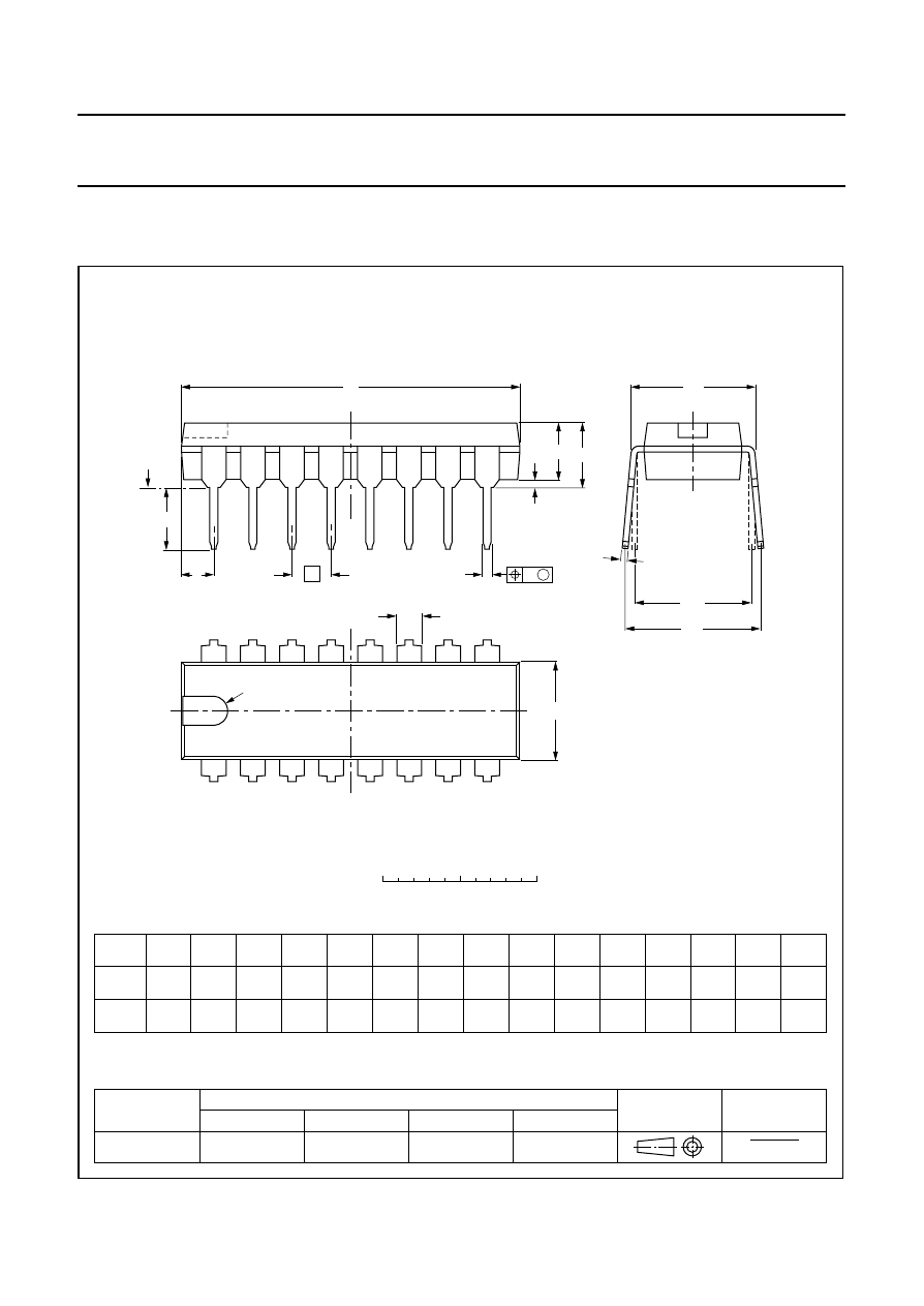
PACKAGE OUTLINES
UNIT
A
max.
1
2
b
1
c
E
e
M
H
L
REFERENCES
OUTLINE
VERSION
EUROPEAN
PROJECTION
ISSUE DATE
IEC
JEDEC
EIAJ
mm
inches
DIMENSIONS (inch dimensions are derived from the original mm dimensions)
SOT38-1
92-10-02
95-01-19
A
min.
A
max.
b
max.
w
M
E
e
1
1.40
1.14
0.055
0.045
0.53
0.38
0.32
0.23
21.8
21.4
0.86
0.84
6.48
6.20
0.26
0.24
3.9
3.4
0.15
0.13
0.254
2.54
7.62
0.30
8.25
7.80
0.32
0.31
9.5
8.3
0.37
0.33
2.2
0.087
4.7
0.51
3.7
0.15
0.021
0.015
0.013
0.009
0.01
0.10
0.020
0.19
050G09
MO-001AE
M
H
c
(e )
1
M
E
A
L
seating plane
A
1
w
M
b
1
e
D
A
2
Z
16
1
9
8
b
E
pin 1 index
0
5
10 mm
scale
Note
1. Plastic or metal protrusions of 0.25 mm maximum per side are not included.
(1)
(1)
D
(1)
Z
DIP16: plastic dual in-line package; 16 leads (300 mil); long body
SOT38-1
1997 Feb 24
10
Philips Semiconductors
Product specification
Radio Data System (RDS) demodulator
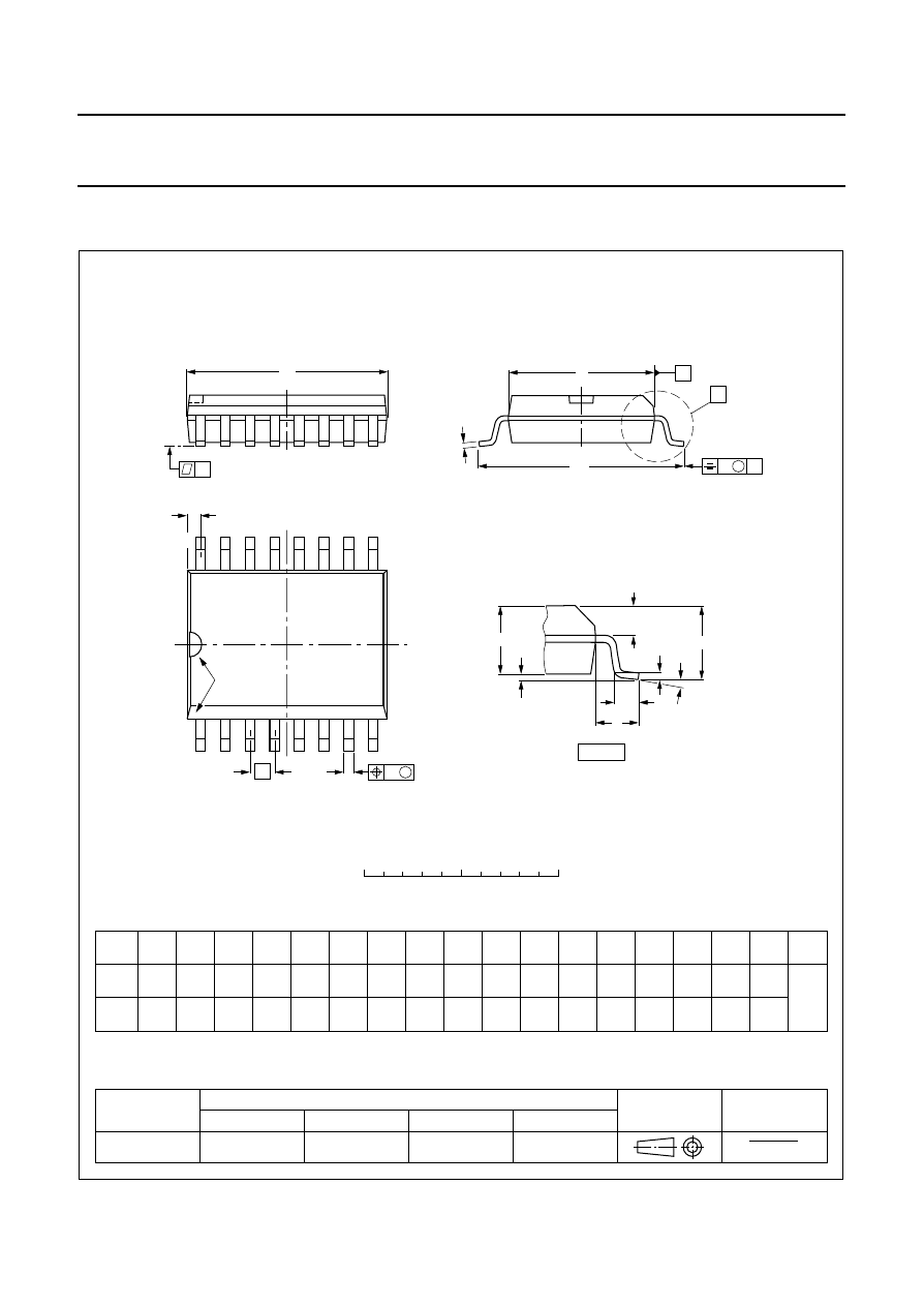
SAA6579
UNIT
A
max.
A
1
A
2
A
3
b
p
c
D
(1)
E
(1)
(1)
e
H
E
L
L
p
Q
Z
y
w
v
Θ
REFERENCES
OUTLINE
VERSION
EUROPEAN
PROJECTION
ISSUE DATE
IEC
JEDEC
EIAJ
mm
inches
2.65
0.30
0.10
2.45
2.25
0.49
0.36
0.32
0.23
10.5
10.1
7.6
7.4
1.27
10.65
10.00
1.1
1.0
0.9
0.4
8
0
o
o
0.25
0.1
DIMENSIONS (inch dimensions are derived from the original mm dimensions)
Note
1. Plastic or metal protrusions of 0.15 mm maximum per side are not included.
1.1
0.4
SOT162-1
8
16
w
M
b
p
D
detail X
Z
e
9
1
y
0.25
075E03
MS-013AA
pin 1 index
0.10
0.012
0.004
0.096
0.089
0.019
0.014
0.013
0.009
0.41
0.40
0.30
0.29
0.050
1.4
0.055
0.42
0.39
0.043
0.039
0.035
0.016
0.01
0.25
0.01
0.004
0.043
0.016
0.01
X
Θ
A
A
1
A
2
H
E
L
p
Q
E
c
L
v
M
A
(A )
3
A
0
5
10 mm
scale
92-11-17
95-01-24
SO16: plastic small outline package; 16 leads; body width 7.5 mm
SOT162-1

1997 Feb 24
11
Philips Semiconductors
Product specification
Radio Data System (RDS) demodulator
SAA6579
SOLDERING
Introduction
There is no soldering method that is ideal for all IC
packages. Wave soldering is often preferred when
through-hole and surface mounted components are mixed
on one printed-circuit board. However, wave soldering is
not always suitable for surface mounted ICs, or for
printed-circuits with high population densities. In these
situations reflow soldering is often used.
This text gives a very brief insight to a complex technology.
A more in-depth account of soldering ICs can be found in
our
IC Package Databook (order code 9398 652 90011).
DIP
S
OLDERING BY DIPPING OR BY WAVE
The maximum permissible temperature of the solder is
260
°
C; solder at this temperature must not be in contact
with the joint for more than 5 seconds. The total contact
time of successive solder waves must not exceed
5 seconds.
The device may be mounted up to the seating plane, but
the temperature of the plastic body must not exceed the
specified maximum storage temperature (T
stg max
). If the
printed-circuit board has been pre-heated, forced cooling
may be necessary immediately after soldering to keep the
temperature within the permissible limit.
R
EPAIRING SOLDERED JOINTS
Apply a low voltage soldering iron (less than 24 V) to the
lead(s) of the package, below the seating plane or not
more than 2 mm above it. If the temperature of the
soldering iron bit is less than 300
°
C it may remain in
contact for up to 10 seconds. If the bit temperature is
between 300 and 400
°
C, contact may be up to 5 seconds.
SO
R
EFLOW SOLDERING
Reflow soldering techniques are suitable for all SO
packages.
Reflow soldering requires solder paste (a suspension of
fine solder particles, flux and binding agent) to be applied
to the printed-circuit board by screen printing, stencilling or
pressure-syringe dispensing before package placement.
Several techniques exist for reflowing; for example,
thermal conduction by heated belt. Dwell times vary
between 50 and 300 seconds depending on heating
method. Typical reflow temperatures range from
215 to 250
°
C.
Preheating is necessary to dry the paste and evaporate
the binding agent. Preheating duration: 45 minutes at
45
°
C.
W
AVE SOLDERING
Wave soldering techniques can be used for all SO
packages if the following conditions are observed:
A double-wave (a turbulent wave with high upward
pressure followed by a smooth laminar wave) soldering
technique should be used.
The longitudinal axis of the package footprint must be
parallel to the solder flow.
The package footprint must incorporate solder thieves at
the downstream end.
During placement and before soldering, the package must
be fixed with a droplet of adhesive. The adhesive can be
applied by screen printing, pin transfer or syringe
dispensing. The package can be soldered after the
adhesive is cured.
Maximum permissible solder temperature is 260
°
C, and
maximum duration of package immersion in solder is
10 seconds, if cooled to less than 150
°
C within
6 seconds. Typical dwell time is 4 seconds at 250
°
C.
A mildly-activated flux will eliminate the need for removal
of corrosive residues in most applications.
R
EPAIRING SOLDERED JOINTS
Fix the component by first soldering two diagonally-
opposite end leads. Use only a low voltage soldering iron
(less than 24 V) applied to the flat part of the lead. Contact
time must be limited to 10 seconds at up to 300
°
C.
When using a dedicated tool, all other leads can be
soldered in one operation within 2 to 5 seconds between
270 and 320
°
C.
1997 Feb 24
12
Philips Semiconductors
Product specification
Radio Data System (RDS) demodulator
SAA6579
DEFINITIONS
LIFE SUPPORT APPLICATIONS
These products are not designed for use in life support appliances, devices, or systems where malfunction of these
products can reasonably be expected to result in personal injury. Philips customers using or selling these products for
use in such applications do so at their own risk and agree to fully indemnify Philips for any damages resulting from such
improper use or sale.
Data sheet status
Objective specification
This data sheet contains target or goal specifications for product development.
Preliminary specification
This data sheet contains preliminary data; supplementary data may be published later.
Product specification
This data sheet contains final product specifications.
Limiting values
Limiting values given are in accordance with the Absolute Maximum Rating System (IEC 134). Stress above one or
more of the limiting values may cause permanent damage to the device. These are stress ratings only and operation
of the device at these or at any other conditions above those given in the Characteristics sections of the specification
is not implied. Exposure to limiting values for extended periods may affect device reliability.
Application information
Where application information is given, it is advisory and does not form part of the specification.

1997 Feb 24
13
Philips Semiconductors
Product specification
Radio Data System (RDS) demodulator
SAA6579
NOTES

1997 Feb 24
14
Philips Semiconductors
Product specification
Radio Data System (RDS) demodulator
SAA6579
NOTES

1997 Feb 24
15
Philips Semiconductors
Product specification
Radio Data System (RDS) demodulator
SAA6579
NOTES

Internet: http://www.semiconductors.philips.com
Philips Semiconductors - a worldwide company
© Philips Electronics N.V. 1997
SCA53
All rights are reserved. Reproduction in whole or in part is prohibited without the prior written consent of the copyright owner.
The information presented in this document does not form part of any quotation or contract, is believed to be accurate and reliable and may be changed
without notice. No liability will be accepted by the publisher for any consequence of its use. Publication thereof does not convey nor imply any license
under patent- or other industrial or intellectual property rights.
Netherlands: Postbus 90050, 5600 PB EINDHOVEN, Bldg. VB,
Tel. +31 40 27 82785, Fax. +31 40 27 88399
New Zealand: 2 Wagener Place, C.P.O. Box 1041, AUCKLAND,
Tel. +64 9 849 4160, Fax. +64 9 849 7811
Norway: Box 1, Manglerud 0612, OSLO,
Tel. +47 22 74 8000, Fax. +47 22 74 8341
Philippines: Philips Semiconductors Philippines Inc.,
106 Valero St. Salcedo Village, P.O. Box 2108 MCC, MAKATI,
Metro MANILA, Tel. +63 2 816 6380, Fax. +63 2 817 3474
Poland: Ul. Lukiska 10, PL 04-123 WARSZAWA,
Tel. +48 22 612 2831, Fax. +48 22 612 2327
Portugal: see Spain
Romania: see Italy
Russia: Philips Russia, Ul. Usatcheva 35A, 119048 MOSCOW,
Tel. +7 095 755 6918, Fax. +7 095 755 6919
Singapore: Lorong 1, Toa Payoh, SINGAPORE 1231,
Tel. +65 350 2538, Fax. +65 251 6500
Slovakia: see Austria
Slovenia: see Italy
South Africa: S.A. PHILIPS Pty Ltd., 195-215 Main Road Martindale,
2092 JOHANNESBURG, P.O. Box 7430 Johannesburg 2000,
Tel. +27 11 470 5911, Fax. +27 11 470 5494
South America: Rua do Rocio 220, 5th floor, Suite 51,
04552-903 São Paulo, SÃO PAULO - SP, Brazil,
Tel. +55 11 821 2333, Fax. +55 11 829 1849
Spain: Balmes 22, 08007 BARCELONA,
Tel. +34 3 301 6312, Fax. +34 3 301 4107
Sweden: Kottbygatan 7, Akalla, S-16485 STOCKHOLM,
Tel. +46 8 632 2000, Fax. +46 8 632 2745
Switzerland: Allmendstrasse 140, CH-8027 ZÃRICH,
Tel. +41 1 488 2686, Fax. +41 1 481 7730
Taiwan: Philips Semiconductors, 6F, No. 96, Chien Kuo N. Rd., Sec. 1,
TAIPEI, Taiwan Tel. +886 2 2134 2870, Fax. +886 2 2134 2874
Thailand: PHILIPS ELECTRONICS (THAILAND) Ltd.,
209/2 Sanpavuth-Bangna Road Prakanong, BANGKOK 10260,
Tel. +66 2 745 4090, Fax. +66 2 398 0793
Turkey: Talatpasa Cad. No. 5, 80640 GÃLTEPE/ISTANBUL,
Tel. +90 212 279 2770, Fax. +90 212 282 6707
Ukraine: PHILIPS UKRAINE, 4 Patrice Lumumba str., Building B, Floor 7,
252042 KIEV, Tel. +380 44 264 2776, Fax. +380 44 268 0461
United Kingdom: Philips Semiconductors Ltd., 276 Bath Road, Hayes,
MIDDLESEX UB3 5BX, Tel. +44 181 730 5000, Fax. +44 181 754 8421
United States: 811 East Arques Avenue, SUNNYVALE, CA 94088-3409,
Tel. +1 800 234 7381
Uruguay: see South America
Vietnam: see Singapore
Yugoslavia: PHILIPS, Trg N. Pasica 5/v, 11000 BEOGRAD,
Tel. +381 11 625 344, Fax.+381 11 635 777
For all other countries apply to: Philips Semiconductors, Marketing & Sales Communications,
Building BE-p, P.O. Box 218, 5600 MD EINDHOVEN, The Netherlands, Fax. +31 40 27 24825
Argentina: see South America
Australia: 34 Waterloo Road, NORTH RYDE, NSW 2113,
Tel. +61 2 9805 4455, Fax. +61 2 9805 4466
Austria: Computerstr. 6, A-1101 WIEN, P.O. Box 213,
Tel. +43 1 60 101, Fax. +43 1 60 101 1210
Belarus: Hotel Minsk Business Center, Bld. 3, r. 1211, Volodarski Str. 6,
220050 MINSK, Tel. +375 172 200 733, Fax. +375 172 200 773
Belgium: see The Netherlands
Brazil: see South America
Bulgaria: Philips Bulgaria Ltd., Energoproject, 15th floor,
51 James Bourchier Blvd., 1407 SOFIA,
Tel. +359 2 689 211, Fax. +359 2 689 102
Canada: PHILIPS SEMICONDUCTORS/COMPONENTS,
Tel. +1 800 234 7381
China/Hong Kong: 501 Hong Kong Industrial Technology Centre,
72 Tat Chee Avenue, Kowloon Tong, HONG KONG,
Tel. +852 2319 7888, Fax. +852 2319 7700
Colombia: see South America
Czech Republic: see Austria
Denmark: Prags Boulevard 80, PB 1919, DK-2300 COPENHAGEN S,
Tel. +45 32 88 2636, Fax. +45 31 57 1949
Finland: Sinikalliontie 3, FIN-02630 ESPOO,
Tel. +358 9 615800, Fax. +358 9 61580/xxx
France: 4 Rue du Port-aux-Vins, BP317, 92156 SURESNES Cedex,
Tel. +33 1 40 99 6161, Fax. +33 1 40 99 6427
Germany: HammerbrookstraÃe 69, D-20097 HAMBURG,
Tel. +49 40 23 53 60, Fax. +49 40 23 536 300
Greece: No. 15, 25th March Street, GR 17778 TAVROS/ATHENS,
Tel. +30 1 4894 339/239, Fax. +30 1 4814 240
Hungary: see Austria
India: Philips INDIA Ltd, Shivsagar Estate, A Block, Dr. Annie Besant Rd.
Worli, MUMBAI 400 018, Tel. +91 22 4938 541, Fax. +91 22 4938 722
Indonesia: see Singapore
Ireland: Newstead, Clonskeagh, DUBLIN 14,
Tel. +353 1 7640 000, Fax. +353 1 7640 200
Israel: RAPAC Electronics, 7 Kehilat Saloniki St, TEL AVIV 61180,
Tel. +972 3 645 0444, Fax. +972 3 649 1007
Italy: PHILIPS SEMICONDUCTORS, Piazza IV Novembre 3,
20124 MILANO, Tel. +39 2 6752 2531, Fax. +39 2 6752 2557
Japan: Philips Bldg 13-37, Kohnan 2-chome, Minato-ku, TOKYO 108,
Tel. +81 3 3740 5130, Fax. +81 3 3740 5077
Korea: Philips House, 260-199 Itaewon-dong, Yongsan-ku, SEOUL,
Tel. +82 2 709 1412, Fax. +82 2 709 1415
Malaysia: No. 76 Jalan Universiti, 46200 PETALING JAYA, SELANGOR,
Tel. +60 3 750 5214, Fax. +60 3 757 4880
Mexico: 5900 Gateway East, Suite 200, EL PASO, TEXAS 79905,
Tel. +9-5 800 234 7381
Middle East: see Italy
Printed in The Netherlands
547027/1200/02/pp16
Date of release: 1997 Feb 24
Document order number:
9397 750 00913

