| Secciones |
|---|
| Foros Electrónica |
|
|
| Boletines de correo |
 |
STK4048
XI
SANYO Electric Co., Ltd. Semiconductor Business Headquarters
TOKYO OFFICE Tokyo Bldg., 1-10, 1 Chome, Ueno, Taito-ku, TOKYO, 110 JAPAN
70397HA (ID) / 9148TA No. 29091/8
Ordering number: 2909A
Thick Film Hybrid IC
AF Power Amplifier (Split Power Supply)
(150W min, THD = 0.008%)
Features
The use of a current mirror circuit, cascode circuit, pure
complementary circuit provides low distortion (THD=
0.008%/100kHz LPF ON).
Possible to design electronic supplementary circuits
(pop noise muting at the time of power ON/OFF, load
short protector, thermal shutdown)
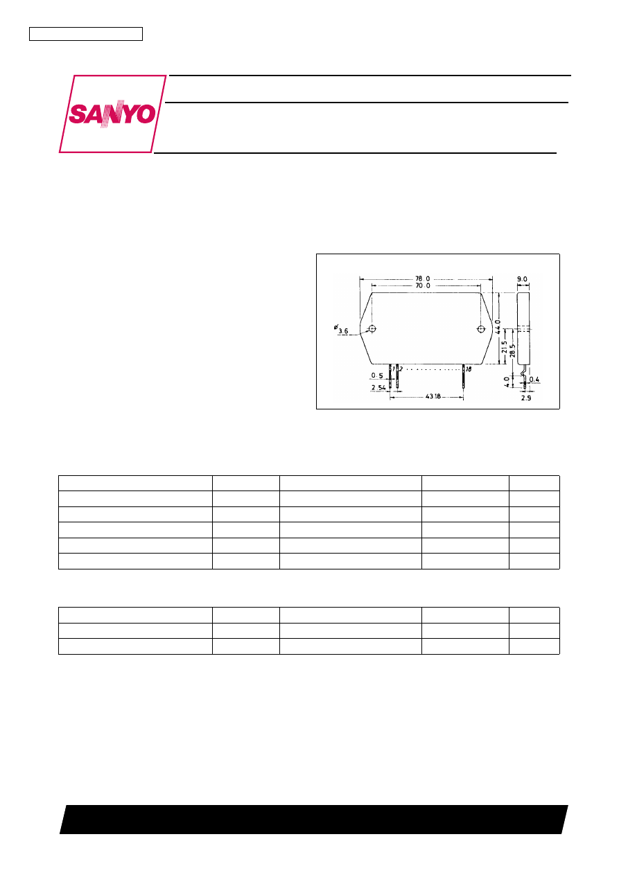
Package Dimensions
unit: mm
4051A
[STK4048
XI
]
Specifications
Maximum Ratings
at Ta = 25
°
C
Recommended Operating Conditions
at Ta = 25
°
C
Parameter
Symbol
Conditions
Ratings
Unit
Maximum supply voltage
V
CC
max
±
87
V
Thermal resistance
Θ
j-c
Per power Transistor
1.2
°
C/W
Junction temperature
Tj
150
°
C
Operating substrate temperature
T
C
125
°
C
Storage temperature
Tstg
-
30 to +125
°
C
Parameter
Symbol
Conditions
Ratings
Unit
Recommended supply voltage
V
CC
±
60
V
Load resistance
R
L
8
Ω¦
STK4048
XI
No. 29092/8
Operating Characteristics
at Ta = 25
°
C, V
CC
=
±
60V, R
L
= 8
Ω¦
, VG = 40dB, Rg = 600
Ω¦
, 100kHz LPF ON,
R
L
: noninductive load
Parameter
Symbol
Conditions
min
typ
max
Unit
Quiescent current
Icco
V
CC
=
±
72V
15
120
mA
Output power
Po
THD = 0.008%,
f = 20Hz to 20kHz
150
W
Total harmonic distortion
THD
Po = 1.0W, f = 1kHz
0.008
%
Frequency response
f
L
, f
H
Po = 1.0W,
dB
20 to 50k
Hz
Input impedance
r
i
Po = 1.0W, f = 1kHz
55
k
Ω¦
Output noise voltage
V
NO
*
V
CC
=
±
72V, Rg = 10k
Ω¦
1.2
mVrms
Neutral voltage
V
N
V
CC
=
±
72V
-70
0
+70
mV
+0
-3
Specified Transformer Power Supply
(Equivalent to MG250)
Notes.
For power supply at the time of test, use a constant-voltage power
supply unless otherwise specified.
*The output noise voltage is represented by the peak value on rms
scale (VTVM) of average value indicating type. The noise voltage
waveform includes no flicker noise. For measurement of the output
noise voltage, use the specified transformer power supply shown
right.
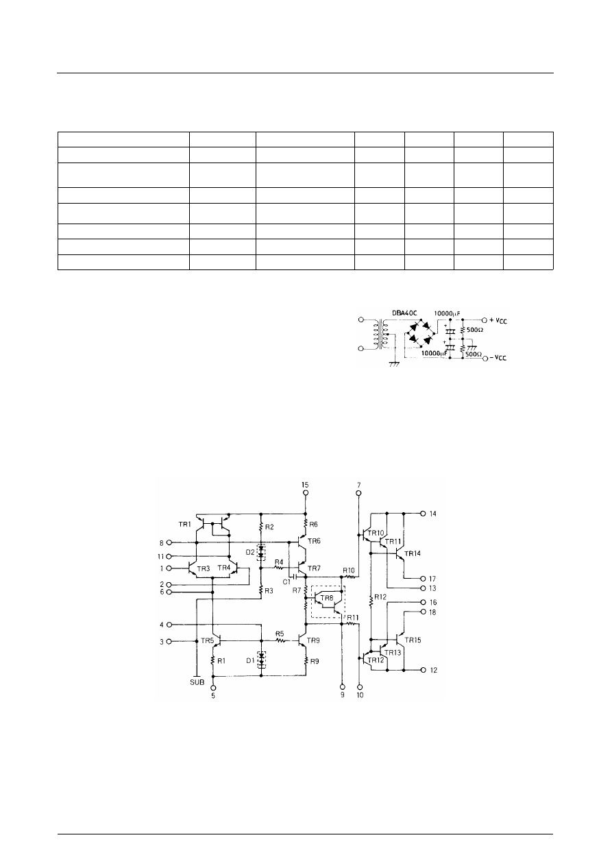
Equivalent Circuit
STK4048
XI
No. 29093/8
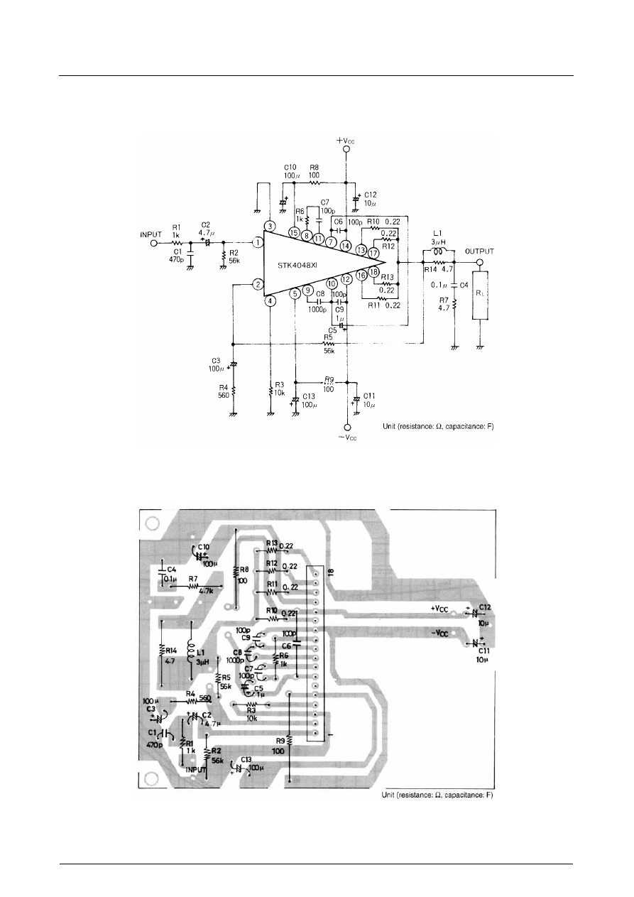
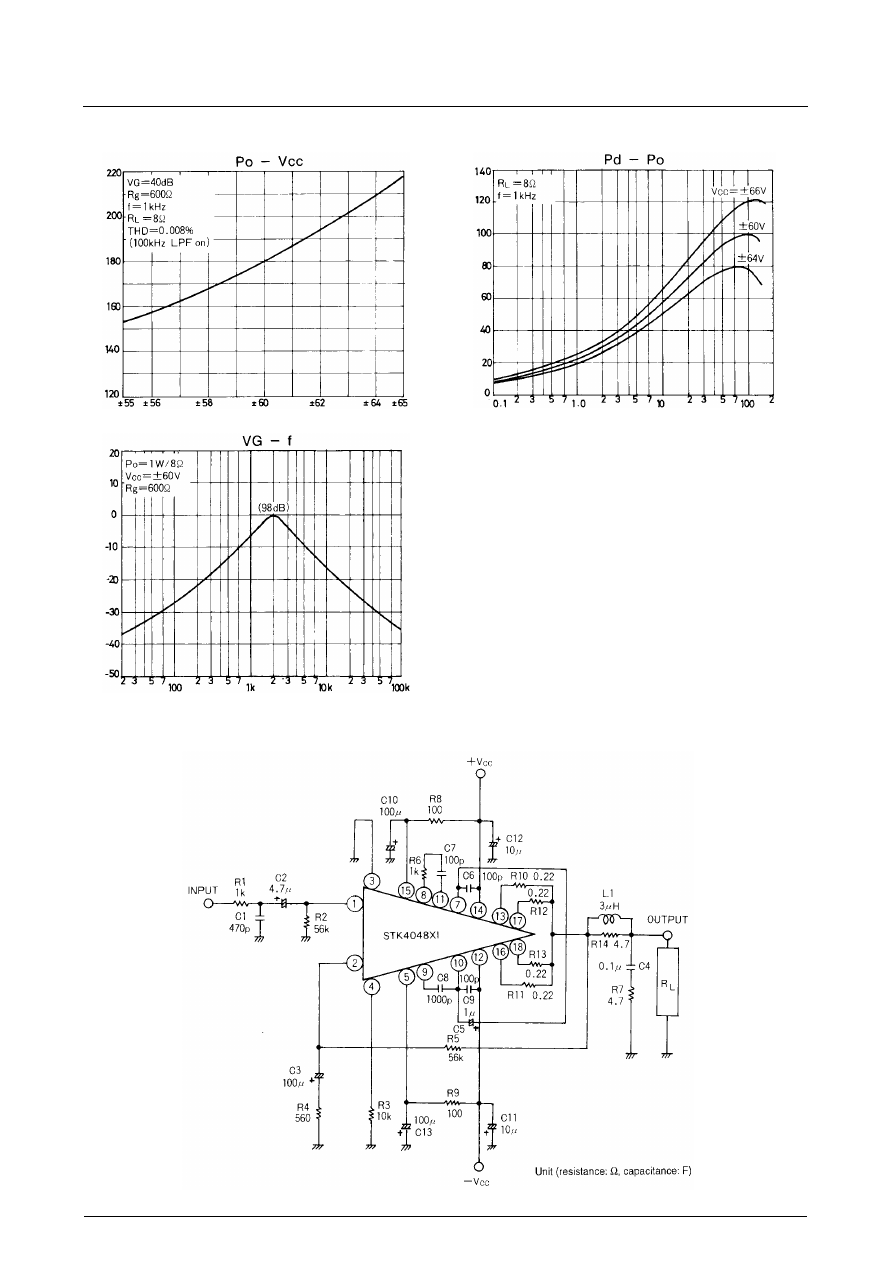
Sample Application Circuit:
150W min Single-Channel AF Power Amplifier
Sample Printed Circuit Pattern for Application Circuit
(Cu-foiled side)
STK4048
XI
No. 29094/8
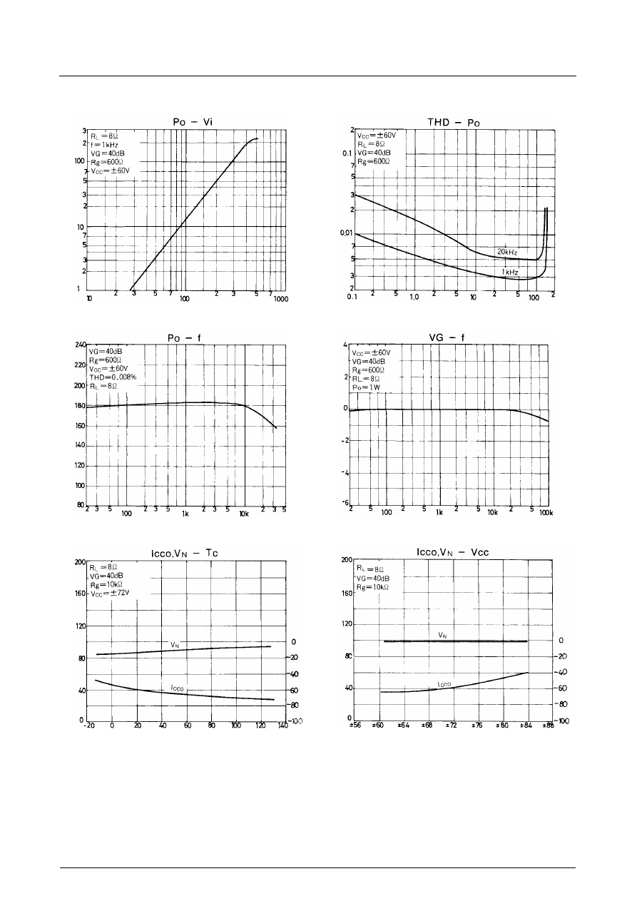
Input voltage, Vi - mV
Frequency, f - Hz
Operating substrate temperature, Tc -
°
C
Output po
wer
, Po -
W
Output po
wer
, Po -
W
Quiescent current, Icco - mA
Neutral v
oltage,
V
N
- mV
Output power, Po - W
Frequency, f - Hz
Supply voltage, V
CC
- V
T
otal harmonic distortion,
THD - %
V
oltage g
ain,
V
G
- dB
Quiescent current, Icco - mA
Neutral v
oltage,
V
N
- mV
STK4048
XI
No. 29095/8
Supply voltage, V
CC
- V
Frequency, f - Hz
Output po
wer
, Po -
W
V
oltage g
ain,
V
G
- dB
Output power, Po - W
IC Po
wer dissipation, Pd -
W
Description of External Parts
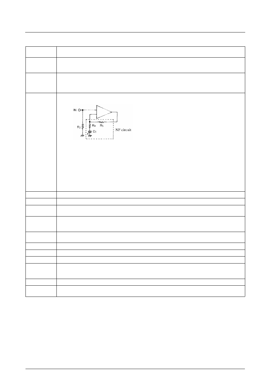
STK4048
XI
No. 29096/8
R1, C1
Input filter circuit
Used to reduce noise at high frequencies.
C2
Input coupling capacitor
Used to block DC current. When the reactance of the capacitor increases at low frequencies, the dependence of 1/f noise on signal source
resistance causes the output noise to worsen. It is better to decrease the reactance.
R2
Input bias resistor
Used to bias the input pin to zero.
Affects V
N
stability. (See NF circuit.)
Because of differential input, this resistor fixes the input resistance practically.
R4, R5
C3 (C2)
NFB circuit (AC NF circuit). It is desirable that the error of the resistor value is 1% or less.
C3
: Capacitor for AC NF
R4, R5
: Used to set VG
VG setting obtained by using R4, R5 . . . . . . . . . . . . . . . . . . . . . . . . . . . . . . . . . . . . .
Low cutoff frequency setting obtained by using, R4, C3. . . . . . . . . . . . . . . . . . . . . . .
Change of VG setting
It is desirable to change R4. In this case, the low cutoff frequency setting needs to be rechecked.
When VG setting is changed by changing R5, R5 must be made equal to R2 to ensure V
N
balance. If the resistor value is increased
more than the existing value, it may be hard to ensure V
N
balance and the temperature characteristic of V
N
may be also deteriorated.
R3
First-stage constant-current bias resistor
R6, C7
Used for oscillation blocking and phase compensation
R7, C4
Used for oscillation blocking and phase compensation
(C4 : A polyester film capacitor is recommended.)
C6, C9
Used for oscillation blocking and phase compensation
(Must be connected near the pin)
C6 : Power amp on (+) side
C9 : Power amp on (-) side
C4
Used for oscillation blocking and phase compensation
(Used for oscillation blocking before clip)
C5
Used for oscillation blocking and distortion improvement
C8, C10
Ripple filter circuit on (+) side
R9, C13
Ripple filter circuit on (-) side
C11, C12
Used for oscillation blocking
Used to decrease the power supply impedance to operate the IC stably. Must be connected near the IC pin. It is desirable to use an
electrolytic capacitor.
L1, R14
Used for oscillation blocking
R10, R11
R12, R13
Output limiting resistors
VG
20
log
R
5
R
4
------
40dBisrecommended
Ë
(
)
=
f
L
2
Ï
R
4
C
3
----------------------------
Hz
( )
=
STK4048
XI
No. 29097/8
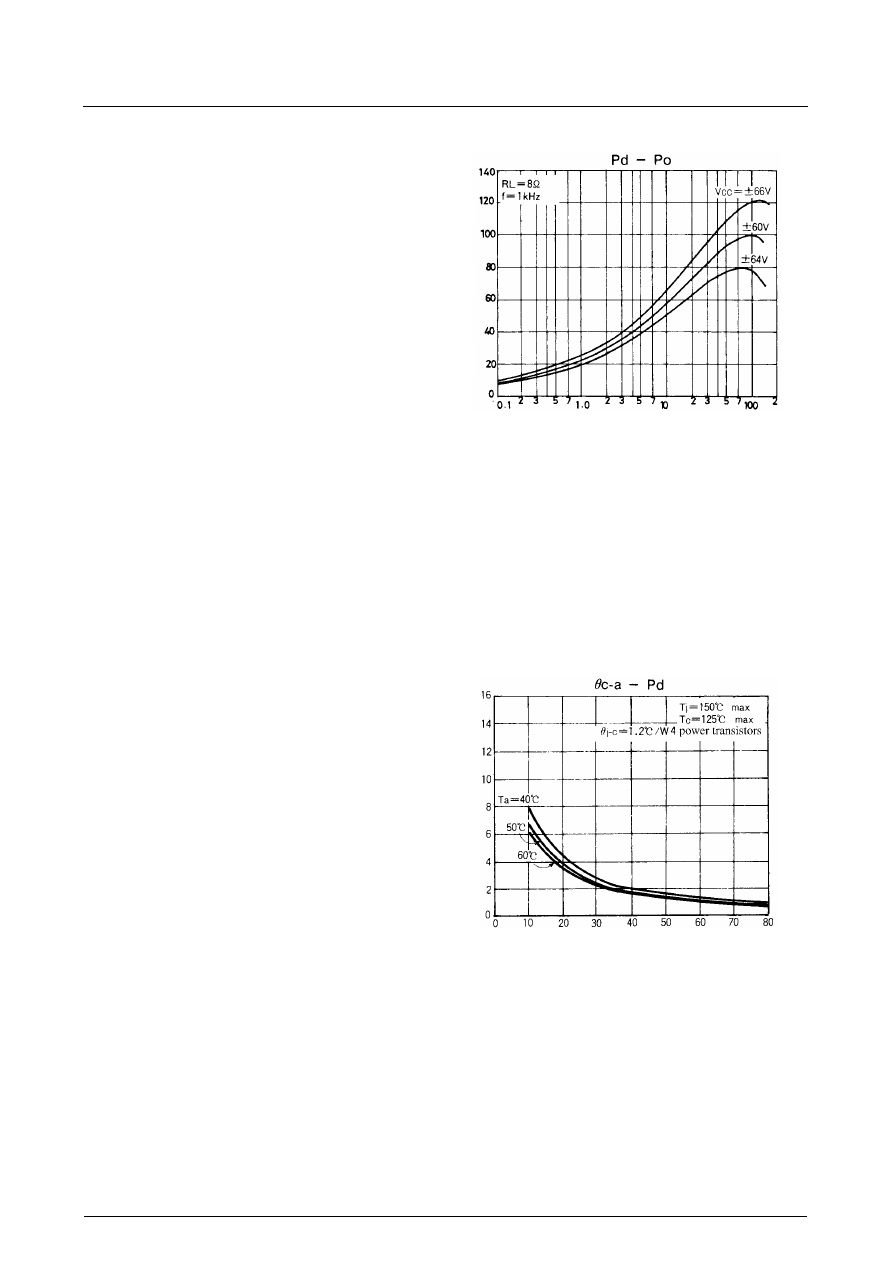
Thermal Design
The IC power dissipation of the STK4048XI at the IC-
operated mode is 100W max. at load resistance 8
Ω¦
for
continuous sine wave as shown in Figure 1.
In an actual application where a music signal is used, it is
impractical to estimate the power dissipation based on the
continuous signal as shown right, because too large a heat
sink must be used. It is reasonable to estimate the power
dissipation as 1/10 Po max. (EIAJ).
That is, Pd = 65W at 8
Ω¦
Thermal resistance
Θ
c-a of a heat sink for this IC power
dissipation (Pd) is fixed under conditions 1 and 2 shown
below.
Figure 1. STK4048XI Pd - Po (R
L
= 8
Ω¦
)
Output power, Po - W
IC Po
wer dissipation, Pd -
W
Condition 1: Tc = Pd
× Θ
c-a + Ta
≤
125
°
C .............................................. (1)
where
Ta : Specified ambient temperature
Tc : Operating substrate temperature
Condition 2: T
j
= Pd
× (Θ
c-a) + Pd/4
× (Θ
j-c) + Ta
≤
150
°
C .................... (2)
where
Tj : Junction temperature of power transistor
Assuming that the power dissipation is shared equally among the four power transistors, thermal resistance
Θ
j-c is
1.2
°
C/W and
Pd
× (Θ
c-a + 1.2/4) + Ta
≤
150
°
C ........................................ (3)
Thermal resistance
Θ
c-a of a heat sink must satisfy ine-
qualities (1) and (3).
Figure 2 shows the relation between Pd and
Θ
c-a given
from (1) and (3) with Ta as a parameter.
[Example] The thermal resistance of a heat sink is
obtained when the ambient temperature speci-
fied for a stereo amplifier is 50
°
C.
Assuming V
CC
=
±
60V, R
L
= 8
Ω¦
,
R
L
= 8
Ω¦
: Pd = 65W at 1/10 Po max.
The thermal resistance of a heat sink is
obtained from Figure 2.
R
L
= 8
Ω¦
:
Θ
c-a1 = 1.15
°
C/W
Tj when a heat sink is used is obtained from
(3).
R
L
= 8
Ω¦
: Tj = 144.3
°
C
Figure 2. STK4048XI
Θ
c-a - Pd
IC Power dissipation, Pd - W
Thermal resistance of heat sink,
Θ
c-a -
°
C/W
This design is based on the use of a constant-voltage regulated power supply. Pd differs when a transformer power supply
is used. Redesign must be made based on Pd that suits the regulation of each transformer.

STK4048
XI
No. 29098/8
No products described or contained herein are intended for use in surgical implants, life-support systems, aerospace equipment, nuclear
power control systems, vehicles, disaster/crime-prevention equipment and the like, the failure of which may directly or indirectly cause injury,
death or property loss.
Anyone purchasing any products described or contained herein for an above-mentioned use shall:
Accept full responsibility and indemnify and defend SANYO ELECTRIC CO., LTD., its affiliates, subsidiaries and distributors and all their
officers and employees, jointly and severally, against any and all claims and litigation and all damages, cost and expenses associated
with such use:
Not impose any responsibility for any fault or negligence which may be cited in any such claim or litigation on SANYO ELECTRIC CO.,
LTD., its affiliates, subsidiaries and distributors or any of their officers and employees, jointly or severally.
Information (including circuit diagrams and circuit parameters) herein is for example only; it is not guaranteed for volume production. SANYO
believes information herein is accurate and reliable, but no guarantees are made or implied regarding its use or any infringements of
intellectual property rights or other rights of third parties.
This catalog provides information as of July, 1997. Specifications and information herein are subject to change without notice.
Document Outline

