| Secciones |
|---|
| Foros Electrónica |
|
|
| Boletines de correo |
 |

TBA820M
1.2W AUDIO AMPLIFIER
DESCRIPTION
The TBA820M is a monolithic integrated audio
amplifier in a 8 lead dual in-line plastic package. It
is intended for use as low frequency class B power
amplifier with wide range of supply voltage: 3 to
16V, in portable radios, cassette recorders and
players etc. Main features are: minimum working
supply voltage of 3V, low quiescent current, low
number of external components, good ripple rejec-
tion, no cross-over distortion, low power dissipa-
tion.
Output power: P
o
= 2W at 12V/8
Ω¦
, 1.6W at 9V/4
Ω¦
and 1.2W at 9V/8
Ω¦
.
June 1988
Minidip
ORDERING NUMBER: TBA820M
Symbol
Parameter
Value
Unit
V
s
Supply voltage
16
V
I
o
Output peak current
1.5
A
P
tot
Power dissipation at T
amb
= 50
°
C
1
W
T
stg
, T
j
Storage and junction temperature
-40 to 150
°
C
ABSOLUTE MAXIMUM RATINGS
TEST AND APPLICATION CIRCUITS
Figure 1. Circuit diagram with load connected to the
supply voltage
Figure 2. Circuit diagram with load connected
to ground
* Capacitor C6 must be used when high rip-
ple
rejection is requested.
1/6
Symbol
Parameter
Value
Unit
R
th-j-amb
Thermal resistance junction-ambient
max
100
°
C/W
THERMAL DATA
2/6
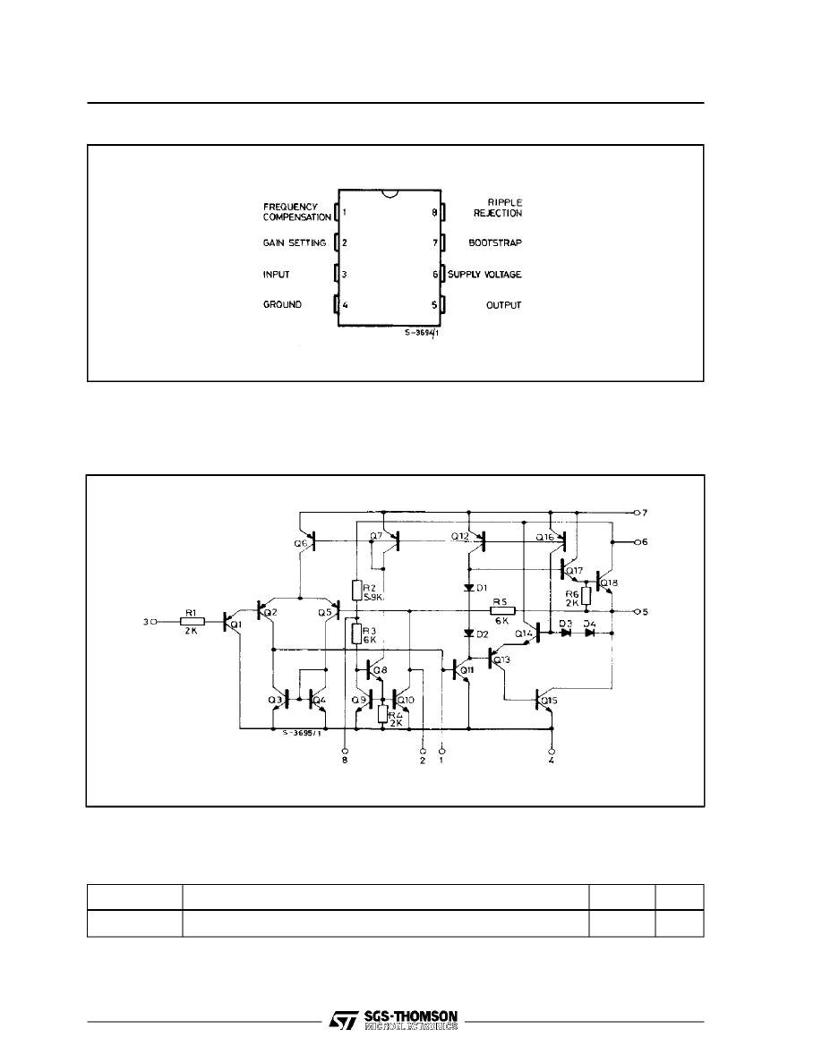
PIN CONNECTION (top view)
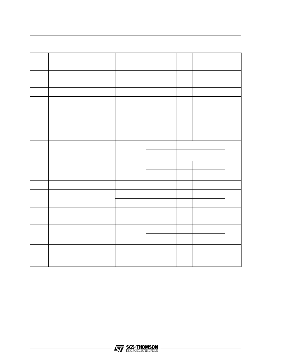
SCHEMATIC DIAGRAM
TBA820M
Symbol
Parameter
Test conditions
Min.
Typ.
Max.
Unit
V
s
Supply voltage
3
16
V
V
o
Quiescent output voltage (pin 5)
4
4.5
5
V
I
d
Quiescent drain current
4
12
mA
I
b
Bias current (pin 3)
0.1
µ
A
P
o
Output power
d = 10%
R
f
= 120
Ω¦
V
s
= 12V
V
s
= 9V
V
s
= 9V
V
s
= 6V
V
s
= 3.5V
f = 1 kHz
R
L
= 8
Ω¦
R
L
= 4
Ω¦
R
L
= 8
Ω¦
R
L
= 4
Ω¦
R
L
= 4
Ω¦
0.9
2
1.6
1.2
0.75
0.25
W
W
W
W
W
Ri
Input resistance (pin 3)
f = 1 kHz
5
M
Ω¦
B
Frequency response (-3 dB)
R
L
= 8
Ω¦
C
5
= 1000
µ
F
R
f
= 120
Ω¦
C
B
= 680 pF
25 to 7,000
Hz
C
B
= 220 pF
25 to 20,000
d
Distortion
P
o
= 500 mW
R
L
= 8
Ω¦
f = 1 kHz
R
f
= 33
Ω¦
0.8
%
R
f
= 120
Ω¦
0.4
G
v
Voltage gain (open loop)
f = 1 kHz
R
L
= 8
Ω¦
75
dB
G
v
Voltage gain (closed loop)
R
L
= 8
Ω¦
R
f
= 33
Ω¦
45
dB
f = 1 kHz
R
f
= 120
Ω¦
34
e
N
Input noise voltage (*)
3
µ
V
i
N
Input noise current (*)
0.4
nA
S
+
N
N
Signal to noise ratio (*)
P
o
= 1.2W
R
L
= 8
Ω¦
G
v
= 34 dB
R1 = 10K
Ω¦
80
dB
R1 = 50 k
Ω¦
70
SVR
Supply voltage rejection
(test circuit of fig. 2)
R
L
= 8
Ω¦
f
(ripple)
= 100 Hz
C6 = 47
µ
F
R
f
= 120
Ω¦
42
dB
ELECTRICAL CHARACTERISTICS
(Refer to the test circuits Vs = 9V, T
amb
= 25
°
C unless otherwise
specified)
(*) B = 22 Hz to 22 KHz
3/6
TBA820M
4/6
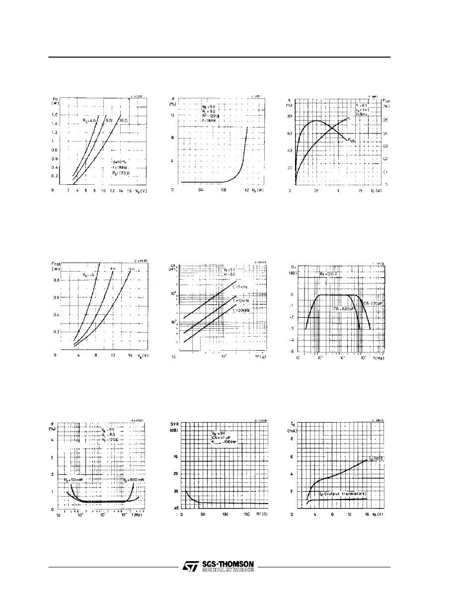
Figure 3. Output power vs.
supply voltage
Figure 4. Harmonic distortion
vs. output power
Figure 5. Power dissipation
and ef ficiency vs. output
power
Figure 6. Maximum power
d i ss i p at i on
(s i ne
wa ve
operation)
Figure 7. Suggested value of
C
B
vs. R
f
Figur e 8. Frequ ency res-
ponse
Figure 9. Harmonic distortion
vs. frequency
Figure 10. Supply voltage
rejection (Fig. 2 circuit)
Figure 11. Quiescent current
vs. supply voltage
TBA820M
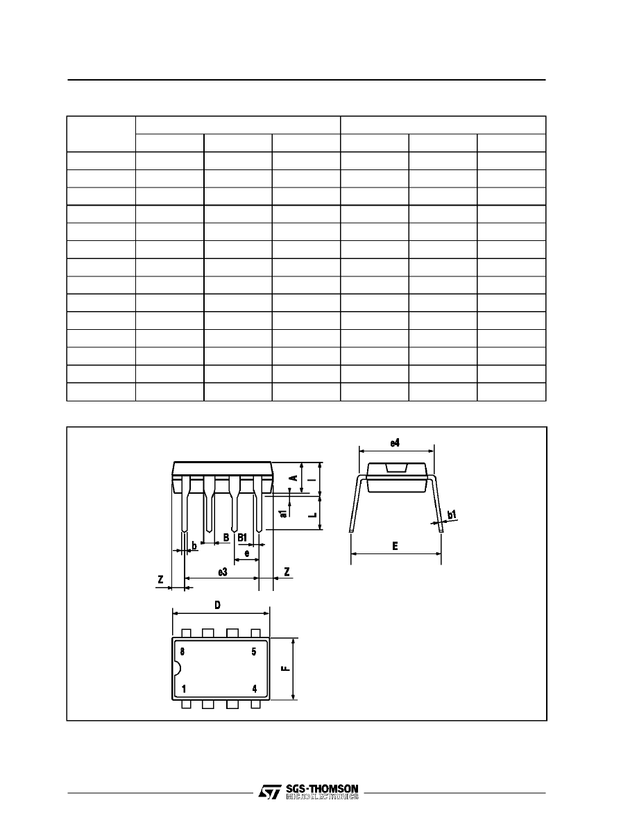
DIM.
mm
inch
MIN.
TYP.
MAX.
MIN.
TYP.
MAX.
A
3.32
0.131
a1
0.51
0.020
B
1.15
1.65
0.045
0.065
b
0.356
0.55
0.014
0.022
b1
0.204
0.304
0.008
0.012
D
10.92
0.430
E
7.95
9.75
0.313
0.384
e
2.54
0.100
e3
7.62
0.300
e4
7.62
0.300
F
6.6
0.260
I
5.08
0.200
L
3.18
3.81
0.125
0.150
Z
1.52
0.060
MINIDIP PACKAGE MECHANICAL DATA
5/6
TBA820M

6/6
Information furnished is believed to be accurate and reliable. However, SGS-THOMSON Microelectronics assumes no responsibility for the
consequences of use of such information nor for any infringement of patents or other rights of third parties which may result from its use. No
license is granted by implication or otherwise under any patent or patent rights of SGS-THOMSON Microelectronics. Specifications mentioned
in this publication are subject to change without notice. This publication supersedes and replaces all information previously supplied.
SGS-THOMSON Microelectronics products are not authorized for use as critical components in life support devices or systems without express
written approval of SGS-THOMSON Microelectronics.
ï
1994 SGS-THOMSON Microelectronics - All Rights Reserved
SGS-THOMSON Microelectronics GROUP OF COMPANIES
Australia - Brazil - France - Germany - Hong Kong - Italy - Japan - Korea - Malaysia - Malta - Morocco - The Netherlands - Singapore -
Spain - Sweden - Switzerland - Taiwan - Thaliand - United Kingdom - U.S.A.
TBA820M

