| Secciones |
|---|
| Foros Electrónica |
|
|
| Boletines de correo |
 |

ï
TDA2003
10W CAR RADIO AUDIO AMPLIFIER
DESCRIPTION
The TDA 2003 has improved performance with the
same pin configuration as the TDA 2002.
The additional features of TDA 2002, very low
number of external components,ease of assembly,
space and cost saving, are maintained.
The device provides a high output current capability
(up to 3.5A) very low harmonic and cross-over
distortion.
Completely safe operation is guaranteed due to
protectionagainst DC and AC short circuit between
all pins and ground, thermal over-range, load dump
voltage surge up to 40V and fortuitous open
ground.
October 1998
Symbol
Parameter
Value
Unit
V
S
Peak supply voltage (50ms)
40
V
V
S
DC supply voltage
28
V
V
S
Operating supply voltage
18
V
I
O
Output peak current (repetitive)
3.5
A
I
O
Output peak current (non repetitive)
4.5
A
Ptot
Power dissipation at Tcase = 90
°
C
20
W
T
stg
, T
j
Storage and junction temeperature
-40 to 150
°
C
ABSOLUTE MAXIMUM RATINGS
TEST CIRCUIT
PENTAWATT
ORDERING NUMBERS : TDA 2003H
TDA 2003V
1/10

Symbol
Parameter
Value
Unit
R
th-j-case
Thermal resistance junction-case
max
3
°
C/W
THERMAL DATA
2/10
PIN CONNECTION (top view)
SCHEMATIC DIAGRAM
TDA2003
Symbol
Parameter
Test conditions
Min.
Typ.
Max.
Unit
DC CHARACTERISTICS (Refer to DC test circuit)
V
s
Supply voltage
8
18
V
V
o
Quiescent output voltage (pin 4)
6.1
6.9
7.7
V
I
d
Quiescent drain current (pin 5)
44
50
mA
AC CHARACTERISTICS (Refer to AC test circuit, Gv = 40 dB)
P
o
Output power
d = 10%
f = 1 kHz
R
L
= 4
Ω¦
R
L
= 2
Ω¦
R
L
= 3.2
Ω¦
R
L
= 1.6
Ω¦
5.5
9
6
10
7.5
12
W
W
W
W
V
i(rms)
Input saturation voltage
300
mV
V
i
Input sensitivity
f = 1 kHz
P
o
= 0.5W
P
o
= 6W
P
o
= 0.5W
P
o
10W
R
L
= 4
Ω¦
R
L
= 4
Ω¦
R
L
= 2
Ω¦
R
L
= 2
Ω¦
14
55
10
50
mV
mV
mV
mV
ELECTRICAL CHARACTERISTICS ( V
s
= 14.4V, T
amb
= 25
°
C unless otherwise specified)
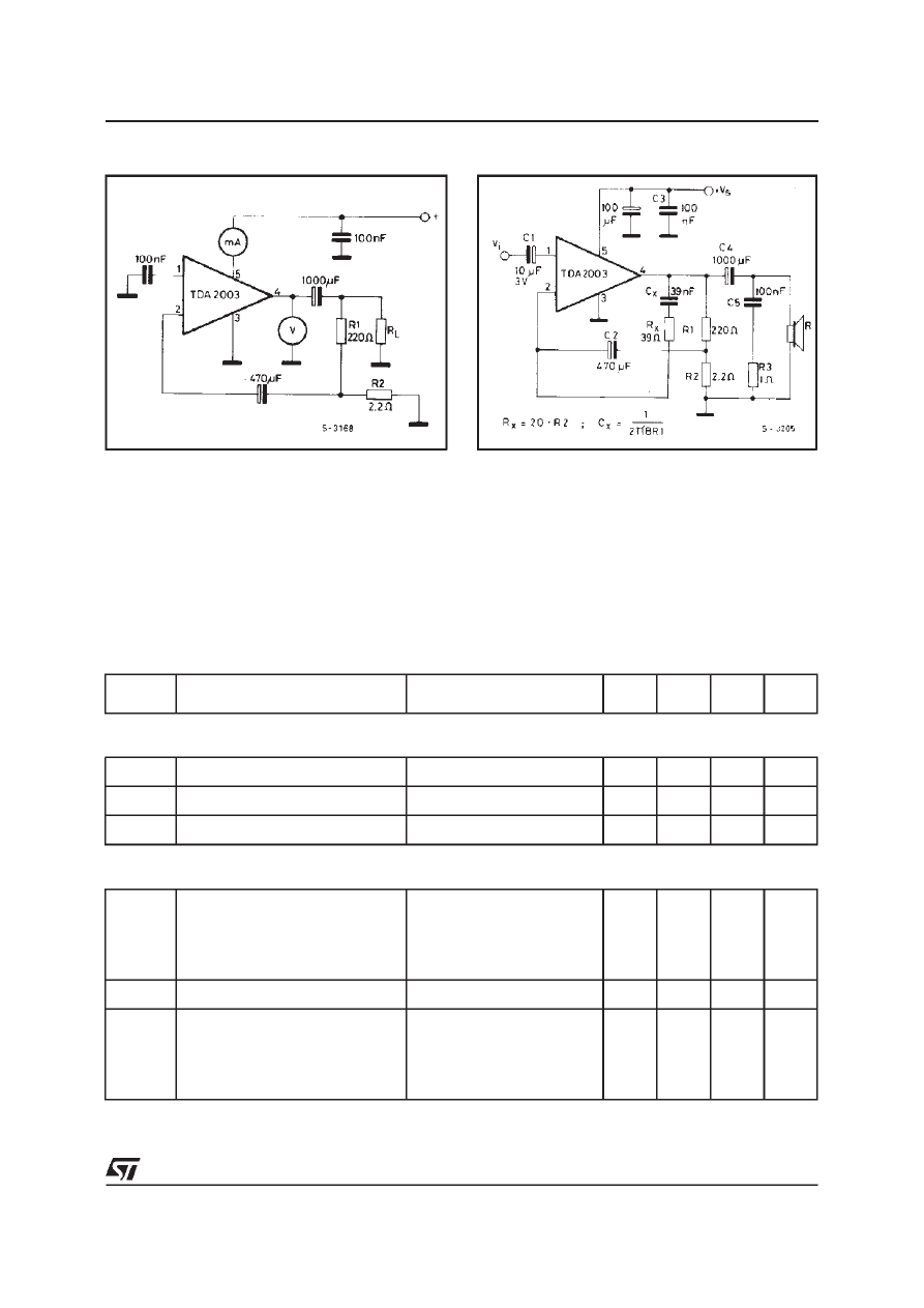
DC TEST CIRCUIT
AC TEST CIRCUIT
3/10
TDA2003
4/10
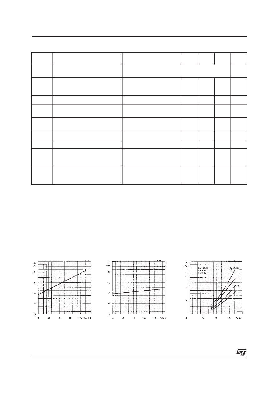
Figure 1. Quiescent output
voltage vs. supply voltage
Figure 2. Quiescent drain
current vs. supply voltage
Figure 3. Output power vs.
supply voltage
Symbol
Parameter
Test conditions
Min.
Typ.
Max.
Unit
B
Frequency response (-3 dB)
P
o
= 1W
R
L
= 4
Ω¦
40 to 15,000
Hz
d
Distortion
f = 1 kHz
P
o
= 0.05 to4.5W R
L
= 4
Ω¦
P
o
= 0.05 to 7.5W R
L
= 2
Ω¦
0.15
0.15
%
%
R
i
Input resistance (pin 1)
f = 1 kHz
70
150
k
Ω¦
G
v
Voltage gain (open loop)
f = 1 kHz
f = 10 kHz
80
60
dB
dB
G
v
Voltage gain (closed loop)
f = 1 kHz
R
L
= 4
Ω¦
39.3
40
40.3
dB
e
N
Input noise voltage
(0)
1
5
µ
V
i
N
Input noise current
(0)
60
200
pA
η
Efficiency
f = 1 Hz
P
o
= 6W
P
o
= 10W
R
L
= 4
Ω¦
R
L
= 2
Ω¦
69
65
%
%
SVR
Supply voltage rejection
f = 100 Hz
V
ripple
= 0.5V
R
g
= 10 k
Ω¦
R
L
= 4
Ω¦
30
36
dB
ELECTRICAL CHARACTERISTICS (continued)
(0) Filter with noise bandwidth: 22 Hz to 22 kHz
TDA2003
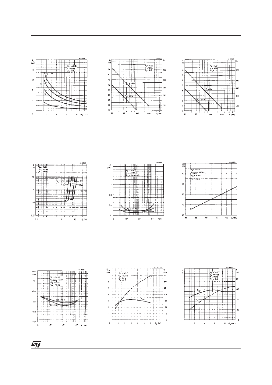
Figure 4. Output power vs.
load resistance R
L
Fi gure 5. Gain vs. inp ut
sensivity
Figure 6. Gain vs. input
sensivity
F i gu re 7. Di st ort ion vs.
output power
Fi g ure 8. D isto r tion vs.
frequency
Figure 9. Supply voltage
rejection vs. voltage gain
Figure 10. Supply voltage
rejection vs. frequency
Figure 11. Power dissipa-
tion and efficiency vs. output
power (R
L
= 4
Ω¦
)
Figure 12. Powe r dissipa-
tion and efficiencyvs. output
power (R
L
= 2
Ω¦
)
5/10
TDA2003
6/10
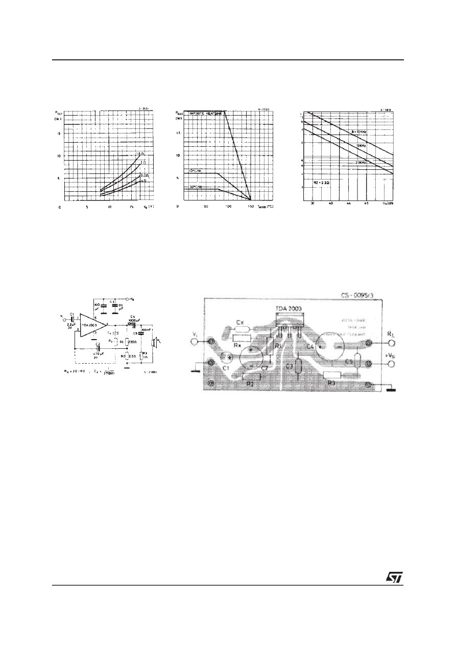
Figure 13. Maximum power
dissipation vs. supply voltage
(sine wave operation)
Figure 14. Maximum allowable
power dissipation vs. ambient
temperature
Figure 15. Typical values of
capacitor (C
X
) for different
values of frequency reponse
(B)
Figure 16. Typical application
circuit
Figure 17. P.C. board and component layout for the circuit of
fig. 16 (1 : 1 scale)
APPLICATION INFORMATION
BUILT-IN PROTECTION SYSTEMS
Load dump voltage surge
The TDA 2003 has a circuit which enables it to
withstand a voltage pulse train, on pin 5, of the type
shown in fig. 19.
If the supply voltage peaks to more than 40V, then
an LC filter must be inserted between the supply
and pin 5, in order to assure that the pulses at pin
5 will be held within the limits shown in fig. 18.
A suggested LC network is shown in fig. 19. With
this network, a train of pulses with amplitude up to
120V and width of 2 ms can be applied at point A.
This type of protection is ON when the supply
voltage(pulsed or DC)exceeds 18V.For this reason
the maximum operating supply voltage is 18V.
TDA2003

Short-circuit (AC and DC conditions)
The TDA 2003 can withstand a permanent short-
circuit on the output for a supply voltage up to 16V.
Polarity inversion
High current (up to 5A) can be handled by the
device with no damage for a longer period than the
blow-out time of a quick 1A fuse (normally con-
nected in series with the supply).
This feature is added to avoid destruction if, during
fitting to the car, a mistake on the connection of the
supply is made.
Open ground
When the radio is in the ON condition and the
ground is accidentally opened, a standard audio
amplifier will be damaged. On the TDA 2003 pro-
tection diodes are included to avoid any damage.
Inductive load
A protection diode is provided between pin 4 and 5
(see the internal schematic diagram) to allow use
of the TDA 2003 with inductive loads.
In particular, the TDA 2003 can drive a coupling
transformer for audio modulation.
DC voltage
The maximum operating DC voltage on the TDA
2003 is 18V.
However the device can withstand a DC voltage up
to 28V with no damage. This could occur during
winter if two batteries were series connected to
crank the engine.
Thermal shut-down
The presence of a thermal limiting circuit offers the
following advantages:
1) an overload on the output (even if it is perma-
nent), oran excessive ambient temperature can
be easily withstood.
2) the heat-sink can have a smaller factor com-
pared with that of a conventionalcircuit.
There is no device damage in the case of ex-
cessive junction temperature: all that happens
is that P
o
(and therefore P
tot
) and I
d
are reduced.
Figure 20. Output power and
dr a in
cu r re n t
vs .
c ase
temperature (R
L
= 4
Ω¦
)
Figure 21. Output power and
d r ai n
cu r re n t
vs .
c as e
temperature (R
L
= 2
Ω¦
)
Figure 18.
Figure 19.
7/10
TDA2003
Component
Recommmended
value
Purpose
Larger than
recommended value
Smaller than
recommended value C1
C1
2.2
µ
F
Input DC
decoupling
Noise at switch-on,
switch-off
C2
470
µ
F
Ripple rejection
Degradation of SVR
C3
0.1
µ
F
Supply bypassing
Danger of oscillation
C4
1000
µ
F
Output coupling to load
Higher low frequency
cutoff
C5
0.1
µ
F
Frequency stability
Danger of oscillation at
high frequencies with
inductive loads
C
X
1
2
Ï
B R1
Upper frequency cutoff
Lower bandwidth
Larger bandwidth
R1
(G
v
-1)
R2
Setting of gain
Increase of drain current
R2
2.2
Ω¦
Setting of gain
and SVR
Degradation of SVR
R3
1
Ω¦
Frequency stability
Danger of oscillation at
high frequencies with
inductive loads
R
X
20 R2
Upper frequency cutoff
Poor high frequency
attenuation
Danger of oscillation
PRATICAL CONSIDERATION
Printed circuit board
The layout shown in fig. 17 is recommended. If
different layouts are used, the ground points of
input 1 and input 2 must be well decoupled from
the ground of the output through which a ratherhigh
current flows.
Assembly suggestion
No electrical insulation is required between the
package and the heat-sink.Pin length should be as
short as possible. The soldering temperature must
not exceed 260
°
C for 12 seconds.
Application suggestions
The recommended component values are those
shown in the application circuits of fig.16.
Different values can be used. The following table is
intended to aid the car-radio designer.
8/10
TDA2003
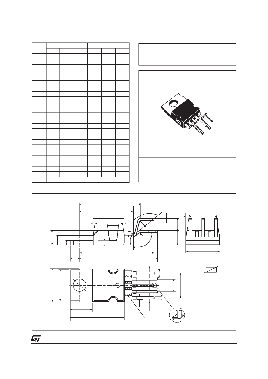
Pentawatt V
DIM.
mm
inch
MIN.
TYP.
MAX.
MIN.
TYP.
MAX.
A
4.8
0.189
C
1.37
0.054
D
2.4
2.8
0.094
0.110
D1
1.2
1.35
0.047
0.053
E
0.35
0.55
0.014
0.022
E1
0.76
1.19
0.030
0.047
F
0.8
1.05
0.031
0.041
F1
1
1.4
0.039
0.055
G
3.2
3.4
3.6
0.126
0.134
0.142
G1
6.6
6.8
7
0.260
0.268
0.276
H2
10.4
0.409
H3
10.05
10.4
0.396
0.409
L
17.55
17.85
18.15
0.691
0.703
0.715
L1
15.55
15.75
15.95
0.612
0.620
0.628
L2
21.2
21.4
21.6
0.831
0.843
0.850
L3
22.3
22.5
22.7
0.878
0.886
0.894
L4
1.29
0.051
L5
2.6
3
0.102
0.118
L6
15.1
15.8
0.594
0.622
L7
6
6.6
0.236
0.260
L9
0.2
0.008
M
4.23
4.5
4.75
0.167
0.177
0.187
M1
3.75
4
4.25
0.148
0.157
0.167
V4
40
°
(typ.)
L
L1
A
C
L5
D1
L2
L3
E
M1
M
D
H3
Dia.
L7
L6
F1
H2
F
G G1
E1
F
E
L9
V4
R
R
R
RESIN BETWEEN
LEADS
H1
V3
H2
L8
V
V
V1
B
V
V
V4
V4
OUTLINE AND
MECHANICAL DATA
9/10
TDA2003

Information furnished is believed to be accurate and reliable. However, STMicroelectronics assumes no responsibility for the consequences of
use of such information nor for any infringement of patents or other rights of third parties which may result from its use. No license is granted
by implication or otherwise under any patent or patent rights of STMicroelectronics. Specification mentioned in this publication are subject to
change without notice. This publication supersedes and replaces all information previously supplied. STMicroelectronics products are not
authorized for use as critical components in life support devices or systems without express written approval of STMicroelectronics.
The ST logo is a registered trademark of STMicroelectronics
ï
1998 STMi croelectronics - Printed in Italy - All Rights Reserved
STMicroelectronics GROUP OF COMPANIES
Australia - Brazil - Canada - China - France - Germany - Italy - Japan - Korea - Malaysia - Malta - Mexico - Morocco - The Netherlands -
Singapore - Spain - Sweden - Switzerland - Taiwan - Thailand - United Kingdom - U.S.A.
http://www.st.com
10/10
TDA2003