| Secciones |
|---|
| Foros Electrónica |
|
|
| Boletines de correo |
 |
TDA7284
RECORD/PLAYBACK CIRCUIT WITH ALC
ADVANCE DATA
WIDE OPERATING SUPPLY VOLTAGE (3V
to 12V)
VERY LOW INPUT NOISE (V
I
= 1.2
µ
V)
INTERNAL
COMPENSATION
FOR
HIGH
GAIN APPLICATION (DOUBLE SPEED RE-
CORDING)
BUILT-IN ALC CIRCUITRY
GOOD SVR
DC CONTROLLED SWITCHES FOR MUTE
OR
EQUALIZATION
SWITCHING
FUNC-
TIONS
DESCRIPTION
The TDA7284 is a monolithic integrated circuit in
a DIP/SO-14 designed for 6V, 9V and 12V AC/DC
portable cassette equipment application.
This is advanced information on a new product now in development or undergoing evaluation. Details are subject to change without notice.
October 1993
DIP14
SO14
ORDERING NUMBER:
TDA7284
TDA7284D
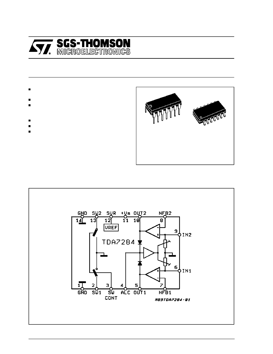
BLOCK DIAGRAM
1/14

Symbol
Parameter
Value
Unit
V
S
Supply Voltage
14
V
T
OP
Operating Temperature Range
-20 to 70
°
C
T
stg
, T
j
Storage and Junction Temperature Range
-40 to 150
°
C
THERMAL DATA
Symbol
Description
S014
DIP14
Unit
R
th j-amb
Thermal Resistance Junction-ambient
Max
200
120
°
C/W
DC CHARACTERISTICS (T
amb
= 25
°
; V
S
= 6V; V
i
= 0V; R
i
= 10K
Ω¦
; ALC = OFF)
Terminal No.
1
2
3
4
5
6
7
8
9
10
11
12
13
14
Terminal Voltage (V)
0
0
0
0
2.6
0
1.3
1.3
0
2.6
6
4.6
0
0
ABSOLUTE MAXIMUM RATINGS
PIN CONNECTION (Top view)
TDA7284
2/14
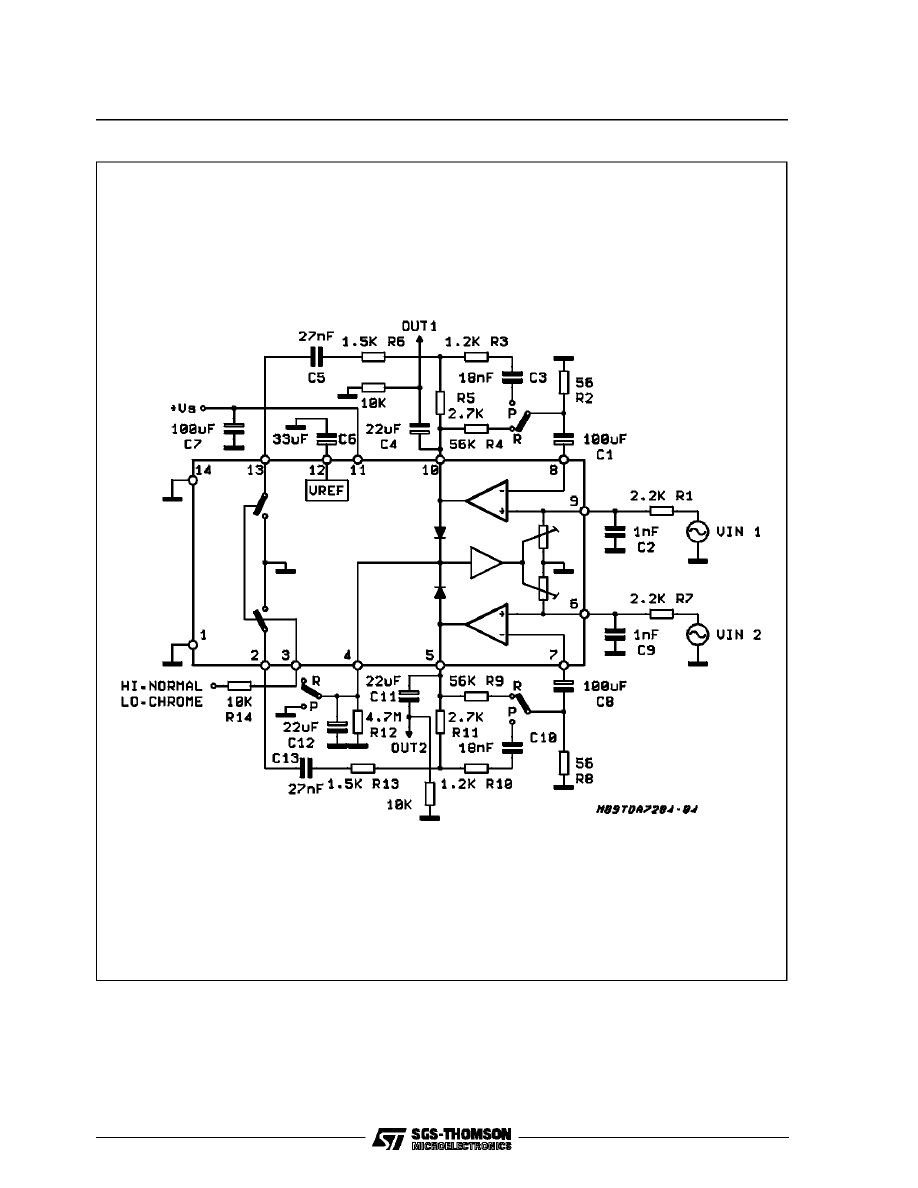
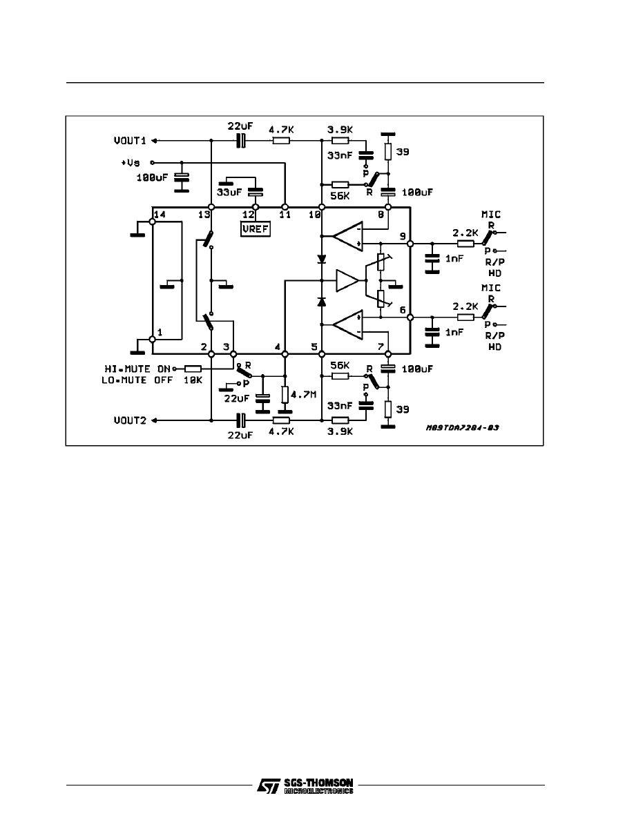
Figure 1: Test and Application Circuit
TDA7284
3/14

Figure 2: P.C. Board and Component Layout of the Circuit of Fig. 1 (1:1 scale).
TDA7284
4/14
ELECTRICAL CHARACTERISTICS (V
S
= 6V, T
amb
= 25
°
C unless otherwise specified refer to test cir-
cuit)
Symbol
Parameter
Test Condition
Min.
Typ.
Max.
Unit
V
S
Supply Voltage
3
12
V
I
d
Quiescent Current
4.5
8
mA
E
n
Input Noise
R
g
= 2.2K
Ω¦
BW = 22Hz to 22kHz
1.2
µ
V
R
I
Input Resistance
30
50
70
K
Ω¦
G
O
Open Loop Gain
65
78
dB
V
O
Output Voltage
THD < 1%
ALC OFF
ALC ON
1.2
0.7
1.8
0.9
1.1
V
rms
V
rms
THD
Total Harmonic Distortion
V
O
= 1V
rms
ALC = ON V
I
= 100mV
0.1
0.3
0.5
1
%
%
ALC Range
∆
V
O
= 3dB
47
dB
CB
Channel Balance
ALC ON
0
2
dB
SVR
Supply Voltage Rejection
f = 120Hz, C
SVR
= 33
µ
F
V
R
= 100mV, R
g
= 10K
Ω¦
ALC = Off
50
dB
CS
Cross-talk
ALC OFF
70
dB
Pin 3
Turn Off Threshold
I
O
= <1
µ
A
0.8
1.3
V
Pin 3
Turn On Threshold
1.7
2.25
V
Pin 3
Turn On Saturation
R
L
= 10K
Ω¦
0.1
0.2
V
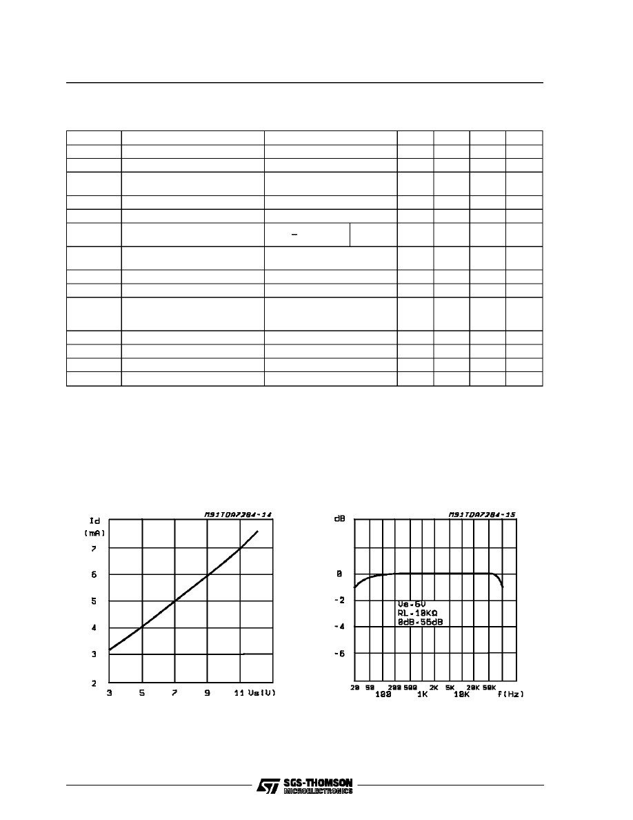
Figure 3: Drain Current vs. Supply Voltage
Figure 4: Recording Closed Loop Gain vs.
Frequency
TDA7284
5/14
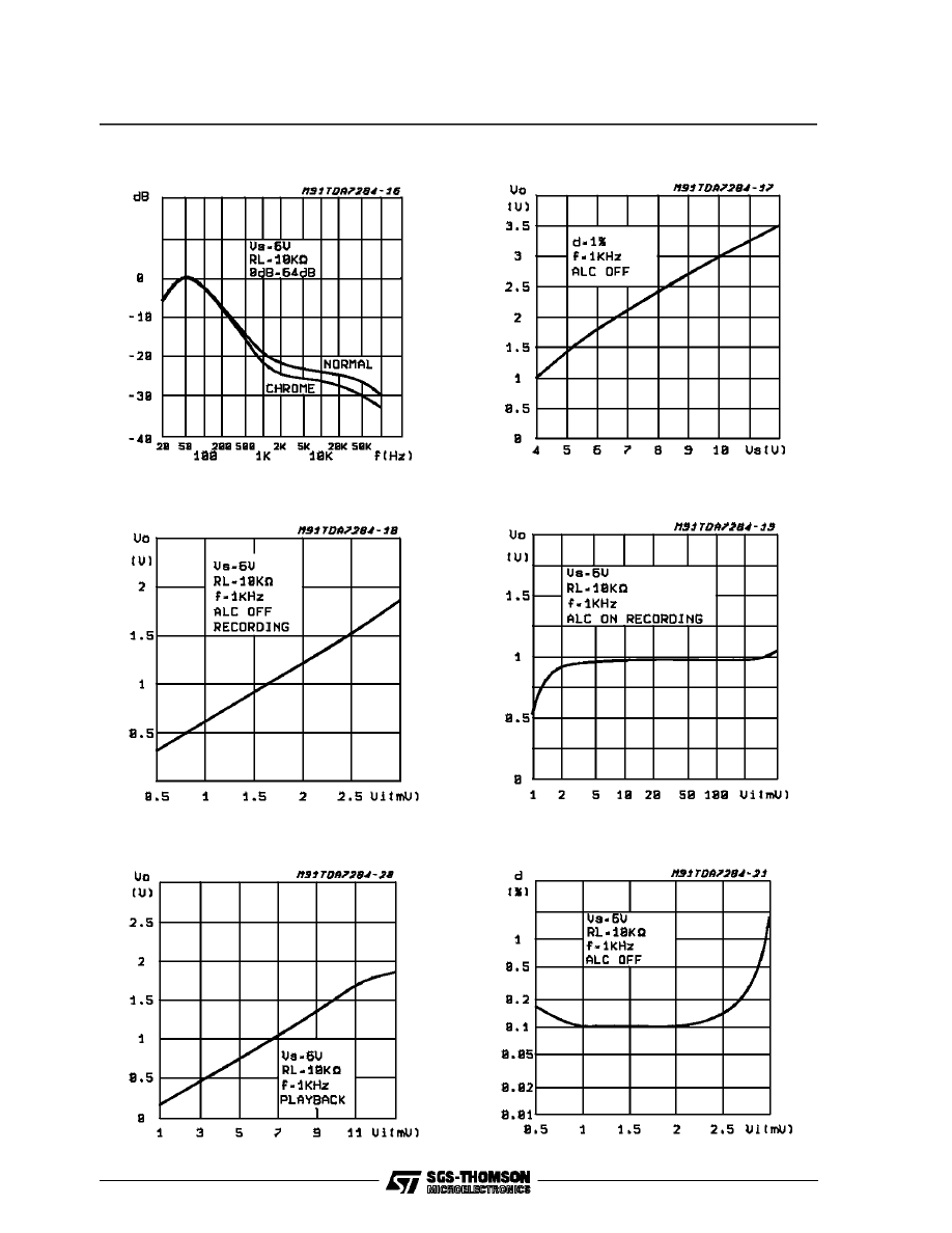
Figure 7: Output Voltage vs. Input Voltage
Figure 8: Output Voltage vs. Input Voltage
Figure 5: Playback Closed Loop Gain vs
Frequency
Figure 6: Normalized Output Voltage vs. Supply
Voltage
Figure 9: Output Voltage vs. Input Voltage
Figure 10: Distortion vs. Input Voltage
TDA7284
6/14
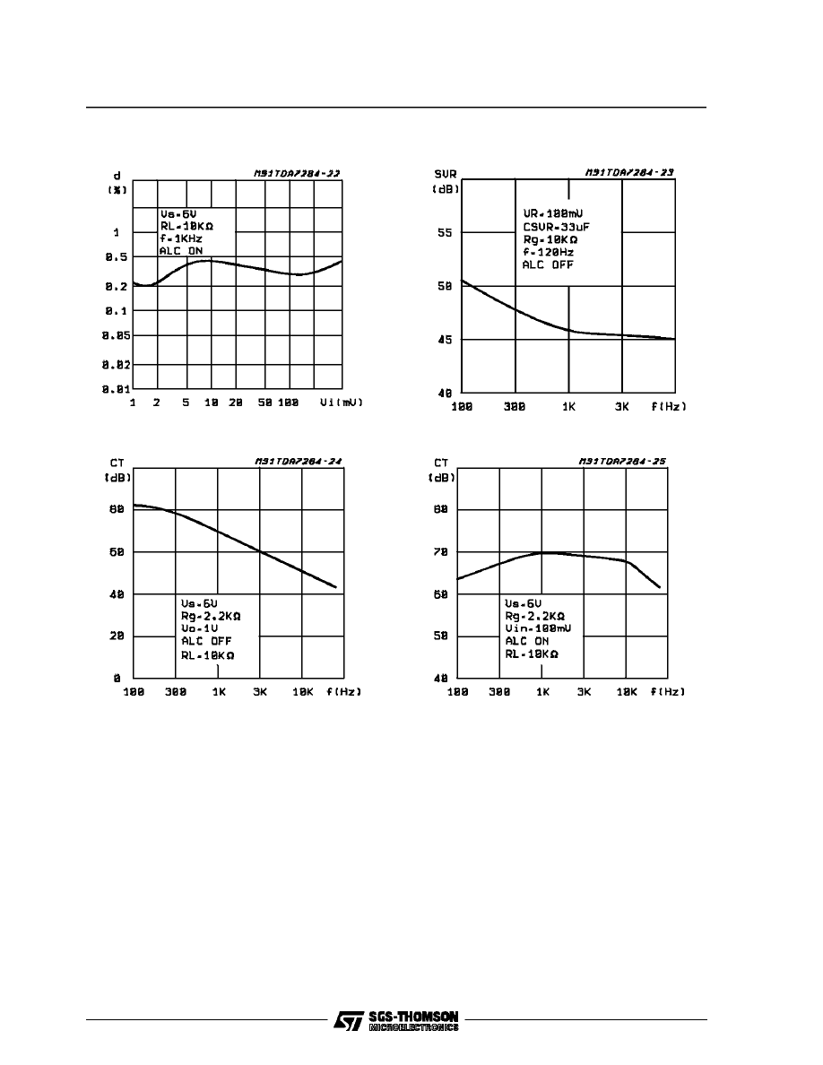
Figure 13: Crosstalk vs. Frequency (ALC = Off)
Figure 14: Crosstalk vs. Frequency (ALC = Off)
Figure 11: Distortion vs. Input Voltage
Figure 12: SVR vs. Frequency (ALC = Off)
TDA7284
7/14
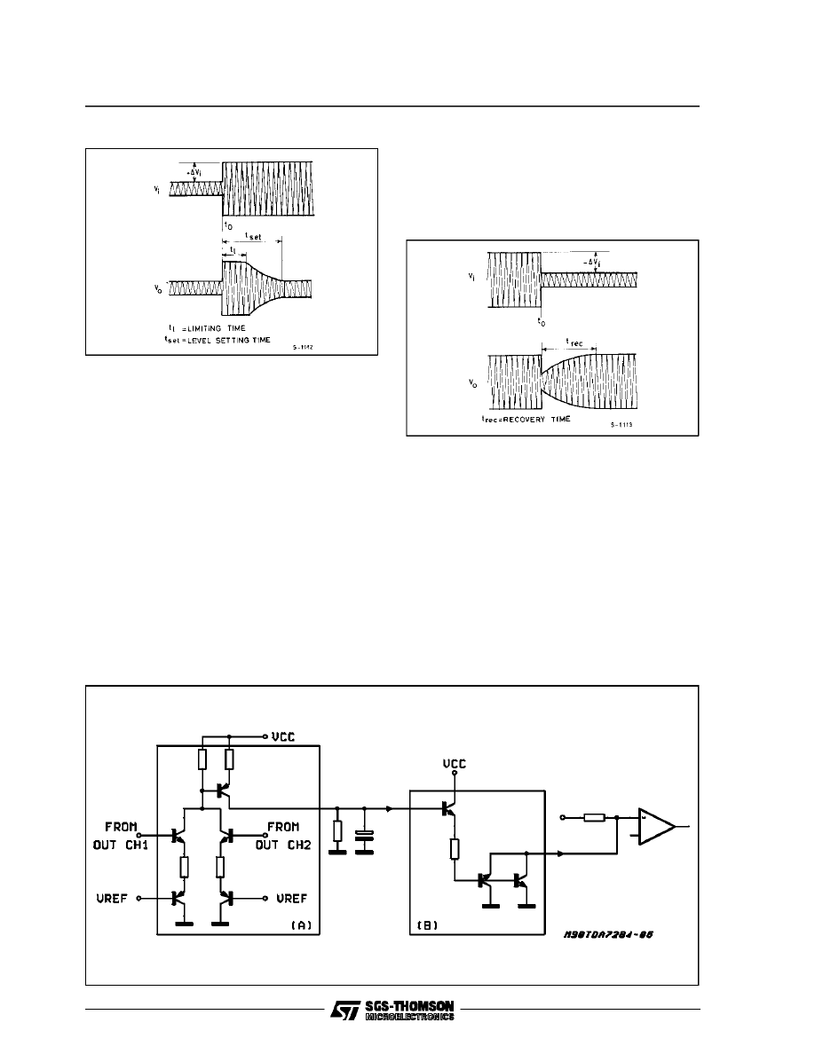
CIRCUIT DESCRIPTION
OPERATIONAL AMPLIFIER
The operational amplifier consists essentially of a
very low noise input stage decoupled from the
single-ended output stage by means of an emitter
follower (fig. 15 ).
The compensations provided in order to have
high gain bandwith product allowing the use for
double speed recording application.
AUTOMATIC LEVEL CONTROL SYSTEM (ALC)
This system maintains the level of the signal to be
recorded at a value which prevents saturation of
the tape and which optimizes the signal to noise
ratio even there are notable variations in the input
signal.
Before presenting the ALC circuit of TDA7284 it is
worth describing the operation of the automatic
level control as a system.A diagram showing the
basis of operation is given in fig.16.
This consists of an amplifier (op-amp) having con-
stant gain (G
V
= 1+R4/R3),which in feedback
transforms output signal level information (usually
by means of a peak-to-peak detector) into a con-
tinuous voltage which drives the networks indi-
cated by T and Rd.
The element T transforms the continuous voltage
level into a signal capable of modifying the circuit
conditions symbolized by variable resistor Rd.
The value assumed by the resistor Rd is a func-
tion of the output signal level Vo and is such that
the voltage Vc at the input of the op-amp is con-
stant,even variations of Vi are present.Obviously
if Vo is less than a certain value the system is not
controlled.
In this case :
V
I
= V
C
=V
O
/ G
V
(G
V
is the gain of the op-amp)
For the TDA7284 the value of V
o
below which the
system is not controlled is around 1 Vrms.
Let us now consider the speed of response of the
system (when controlled) to positive and negative
changes of the input signal i.e. the limiting
time,the time for return to nominal level (1 Vrms)
and the recovery time.
Limiting time, and time for return to nominal
level.
Let us suppose that at certain moment T
o
, the in-
put signal increases by +
∆
Vi as shown in fig. 17.
Figure 15
Figure 16: Basic Diagram of the ALC stage
TDA7284
8/14
Usually such an increase drives the op-amp into
saturation and the time for which it remains in this
condition is called the limiting time(T1).
T1 depends on the relationship between the ex-
ternal capacitances, the time constant T=R1
C1,
the supply voltage and the signal variation.
The criteria for choosing the length of T1 are the
result of several compromises. In particular if T1
is too long, there will be audible distortion during
playback (during T1 the output is a square
wave),and if it is too short, the sensation of in-
creased level will be lost while dynamic compres-
sion phenomena and instability may occur.
The time for return to nominal level is defined as
the total time between the instant To and the in-
stant in which the output reassumes the nominal
value. This time (Ts) is roughly equal to 5
T1.
On the basis of tests carried out it has been found
that a musical signal with high dynamic range
(
∆
V
I
=+40 dB) is to be recorded, the best value of
Ts is between 200 and 300ms.
Recovery time.
let us now suppose that at the instant To the input
signal decreases of
∆
Vi (fig. 18).
The recovery time (Trec) is defined as the time
between the instant To and the instant in which
the output signal returns to the nominal level.
This time depends essentially on the discharge
time constant of R2
C2 ( see fig. 16) and on the
size of the step -
∆
Vi. In this case too, if this time
is too long the signal to noise ratio on the tape de-
teriorates.
If it is too short the sensation of the low signal
level is lost during playback.
The ALC system of the TDA7284
Fig. 16 becomes the following (fig. 19) where the
Figure 17: Limiting and Level Setting Time
Figure 18: Recovery Time
Figure 19
TDA7284
9/14
peak-to-peak detector of fig. 16 is now inside the
broken line 1 while the system which allows a di-
namic resistance varying with the DC voltage
level (i.e. inversely proportional to the op-amp
output signal),is inside the broken line 2.
It should be noted that the generator resistance
Ri
has no influence on the controlled voltage
value Vc, although its value should be between 1
and 47 Kohm.
The lower limit is determined by the minimum dy-
namic resistance
of 10 ohm and therefore to
have a control range of 40 dB for the input signal,
Ri must be greather than 1.5 Kohm.
The upper limit results from the necessity to limit
the attenuation of the signal by the input imped-
ance of the op-amp.
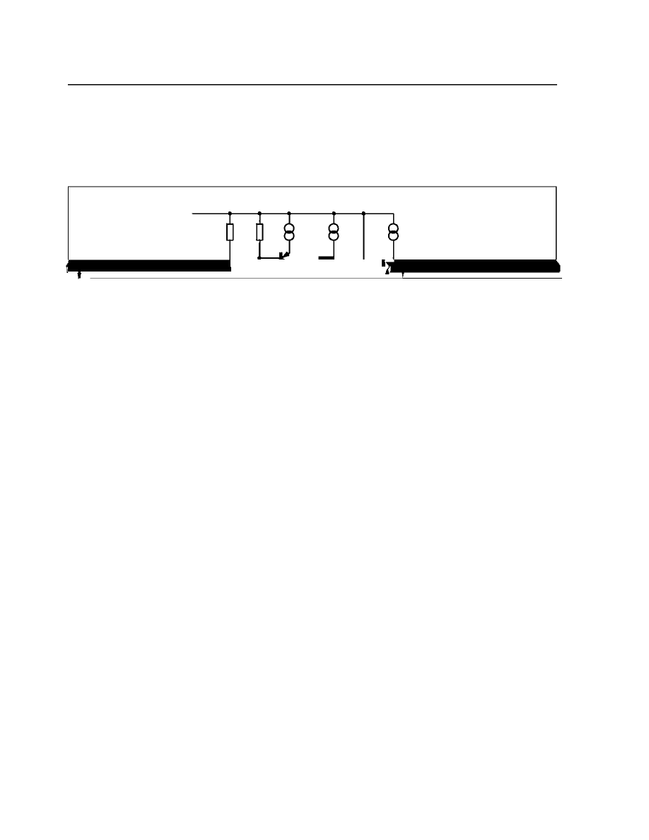
Switches
Two DC-controlled switches are also included in
the chip (fig. 20 )
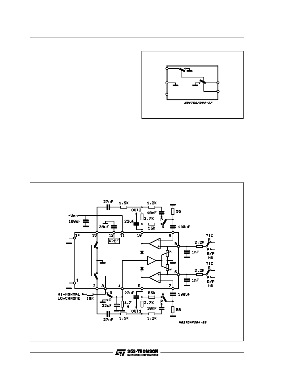
Fig. 19 shows the typical application circuit of the
TDA7284 utilizing the equalization switch for nor-
mal or chrome tape playback equalization.The
advantage is the components can be placed near
to the IC, while the tape selector switch can be at
a remote location, hence reduce the chances of
noise and oscillation due to components layout.
Another advantage is that only one pole is
needed for the tape selector switch as compared
to the two poles needed by conventional circuits
(one separate pole for each channel).
Fig. 22 shows the use of the switches to obtain
the mute function.
Figure 20
Figure 21: Application Circuit with DC Switching of Normal/Chrome Tape Equalization
TDA7284
10/14
SVR
A refernce circuit is enclosed to provide a stable
voltage and to supply a stable current to all cur-
rent mirrors.
SVR capacitor is also connected to this block for
good ripple rejection.
Figure 22: Application Circuit with Output Muting
TDA7284
11/14
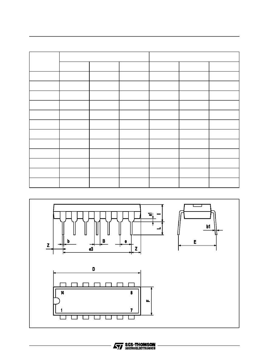
DIP14 PACKAGE MECHANICAL DATA
DIM.
mm
inch
MIN.
TYP.
MAX.
MIN.
TYP.
MAX.
a1
0.51
0.020
B
1.39
1.65
0.055
0.065
b
0.5
0.020
b1
0.25
0.010
D
20
0.787
E
8.5
0.335
e
2.54
0.100
e3
15.24
0.600
F
7.1
0.280
I
5.1
0.201
L
3.3
0.130
Z
1.27
2.54
0.050
0.100
TDA7284
12/14
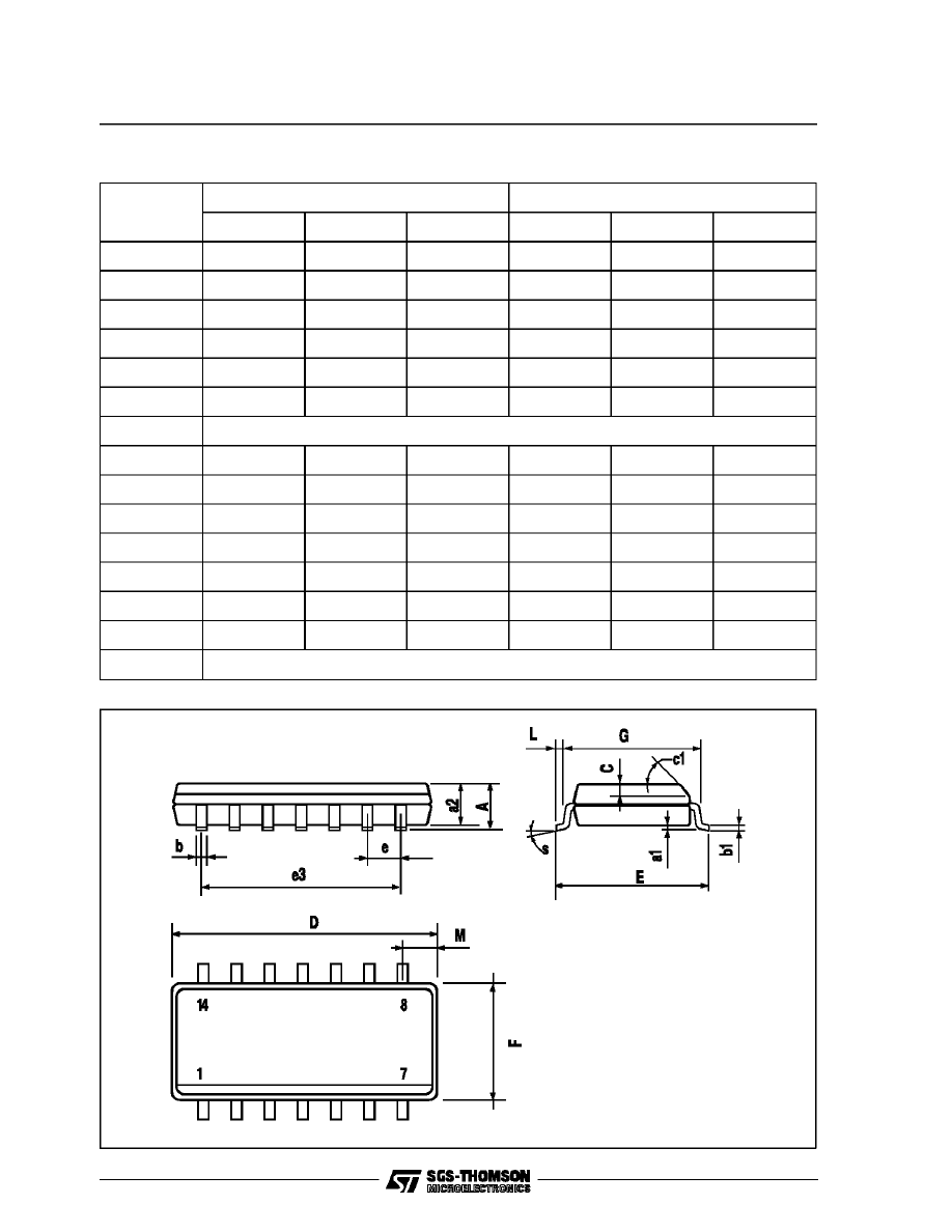
SO14 PACKAGE MECHANICAL DATA
DIM.
mm
inch
MIN.
TYP.
MAX.
MIN.
TYP.
MAX.
A
1.75
0.069
a1
0.1
0.2
0.004
0.008
a2
1.6
0.063
b
0.35
0.46
0.014
0.018
b1
0.19
0.25
0.007
0.010
C
0.5
0.020
c1
45
°
(typ.)
D
8.55
8.75
0.336
0.344
E
5.8
6.2
0.228
0.244
e
1.27
0.050
e3
7.62
0.300
F
3.8
4.0
0.15
0.157
L
0.5
1.27
0.020
0.050
M
0.68
0.027
S
8
°
(max.)
TDA7284
13/14

Information furnished is believed to be accurate and reliable. However, SGS-THOMSON Microelectronics assumes no responsibility for the
consequences of use of such information nor for any infringement of patents or other rights of third parties which may result from its use. No
license is granted by implication or otherwise under any patent or patent rights of SGS-THOMSON Microelectronics. Specifications men-
tioned in this publication are subject to change without notice. This publication supersedes and replaces all information previously supplied.
SGS-THOMSON Microelectronics products are not authorized for use as critical components in life support devices or systems without ex-
press written approval of SGS-THOMSON Microelectronics.
ï
1994 SGS-THOMSON Microelectronics - All Rights Reserved
SGS-THOMSON Microelectronics GROUP OF COMPANIES
Australia - Brazil - France - Germany - Hong Kong - Italy - Japan - Korea - Malaysia - Malta - Morocco - The Netherlands
Singapore - Spain - Sweden - Switzerland - Taiwan - Thaliand - United Kingdom - U.S.A.
TDA7284
14/14

