| Secciones |
|---|
| Foros Electrónica |
|
|
| Boletines de correo |
 |
1
Features
Low-voltage and Standard-voltage Operation
- 2.7 (V
CC
= 2.7V to 5.5V)
- 1.8 (V
CC
= 1.8V to 5.5V)
User-selectable Internal Organization
- 1K: 128 x 8 or 64 x 16
Three-wire Serial Interface
2 MHz Clock Rate (5V)
Self-timed Write Cycle (10 ms max)
High Reliability
- Endurance: 1 Million Write Cycles
- Data Retention: 100 Years
Automotive Grade Devices Available
8-lead JEDEC PDIP, 8-lead JEDEC SOIC, 8-lead EIAJ SOIC, 8-lead Ultra Thin mini-MAP
(MLP 2x3), 8-lead TSSOP and 8-ball dBGA2 Packages
Description
The AT93C46 provides 1024 bits of serial electrically erasable programmable read-
only memory (EEPROM), organized as 64 words of 16 bits each (when the ORG pin is
connected to VCC), and 128 words of 8 bits each (when the ORG pin is tied to
ground). The device is optimized for use in many industrial and commercial applica-
tions where low-power and low-voltage operations are essential. The AT93C46 is
available in space-saving 8-lead PDIP, 8-lead JEDEC SOIC, 8-lead EIAJ SOIC, 8-lead
Ultra Thin mini-MAP (MLP 2x3), 8-lead TSSOP, and 8-lead dBGA2 packages.
The AT93C46 is enabled through the Chip Select pin (CS) and accessed via a
three-wire serial interface consisting of Data Input (DI), Data Output (DO), and Shift
Clock (SK). Upon receiving a Read instruction at DI, the address is decoded and the
data is clocked out serially on the DO pin. The Write cycle is completely self-timed,
and no separate Erase cycle is required before Write. The Write cycle is only enabled
when the part is in the Erase/Write Enable state. When CS is brought high following
the initiation of a Write cycle, the DO pin outputs the Ready/Busy status of the part.
The AT93C46 is available in 2.7V to 5.5V and 1.8V to 5.5V versions.
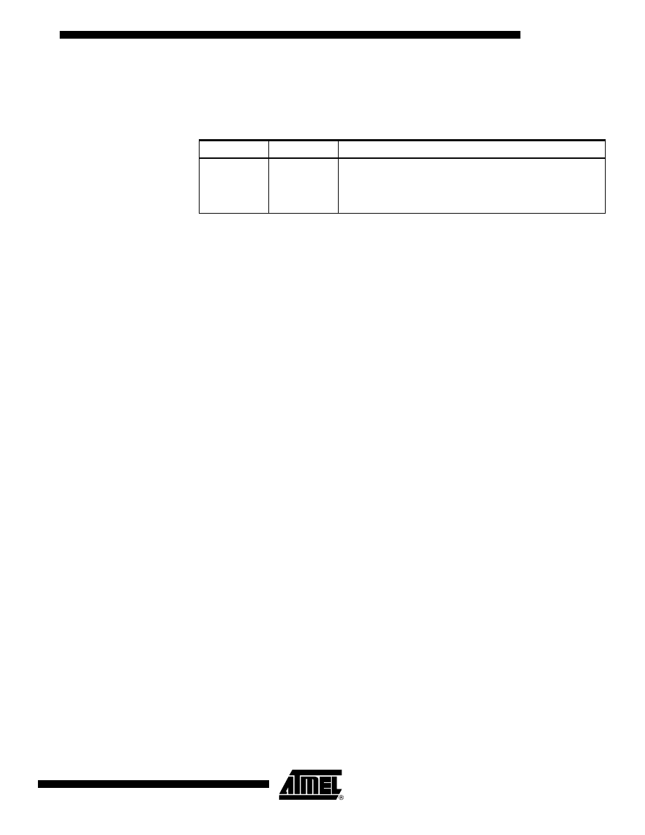
Table 1. Pin Configurations
Pin Name
Function
CS
Chip Select
SK
Serial Data Clock
DI
Serial Data Input
DO
Serial Data Output
GND
Ground
VCC
Power Supply
ORG
Internal Organization
DC
Dont Connect
Three-wire
Serial
EEPROM
1K (128 x 8 or 64 x 16)
AT93C46
Note: Not recommended for new
design; please refer to
AT93C46D datasheet.
5140B-SEEPR-2/07
1
2
3
4
8
7
6
5
CS
SK
DI
DO
VCC
DC
ORG
GND
VCC
DC
ORG
GND
C
S
S
K
D1
D0
1
2
3
4
8
7
6
5
1
2
3
4
8
7
6
5
CS
SK
DI
DO
VCC
DC
ORG
GND
1
2
3
4
8
7
6
5
DC
VCC
CS
SK
ORG
GND
DO
DI
1
2
3
4
8
7
6
5
VCC
DC
ORG
GND
CS
SK
DI
DO
1
2
3
4
8
7
6
5
CS
SK
DI
DO
VCC
DC
ORG
GND
8-lead SOIC
8-lead dBGA2
8-lead PDIP
8-lead SOIC
Rotated (R)
(1K JEDEC Only)
8-lead Ultra Thin mini-MAP (MLP 2x3)
8-lead TSSOP
Bottom View
Bottom View
2
AT93C46
5140B-SEEPR-2/07
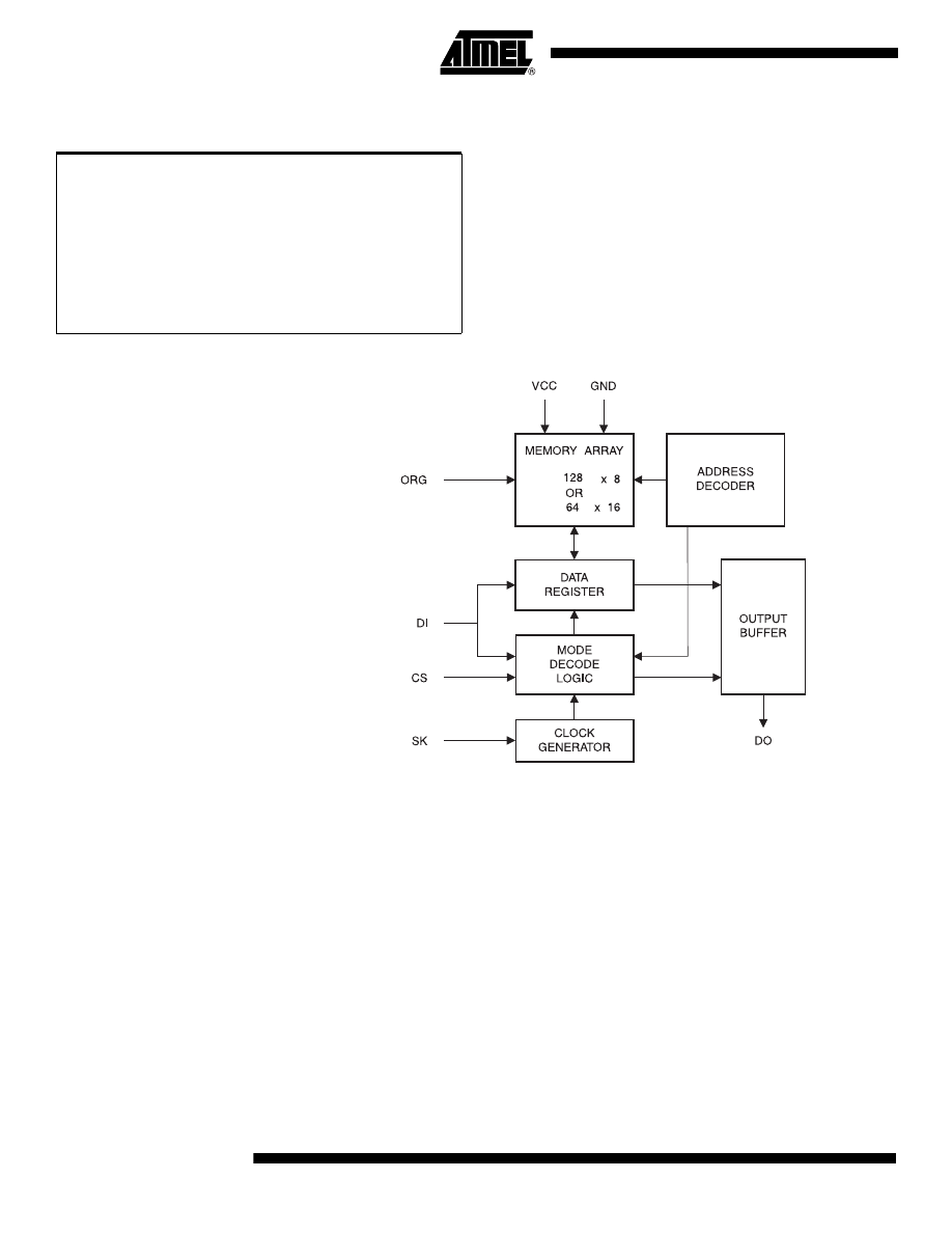
Figure 1. Block Diagram
Note:
When the ORG pin is connected to VCC, the x 16 organization is selected. When it is
connected to ground, the x 8 organization is selected. If the ORG pin is left uncon-
nected and the application does not load the input beyond the capability of the internal 1
Meg ohm pullup, then the x 16 organization is selected. The feature is not available on
the 1.8V devices.
For the AT93C46, if x 16 organization is the mode of choice and Pin 6 (ORG) is left
unconnected, Atmel recommends using the AT93C46A device. For more details, see the
AT93C46A datasheet.
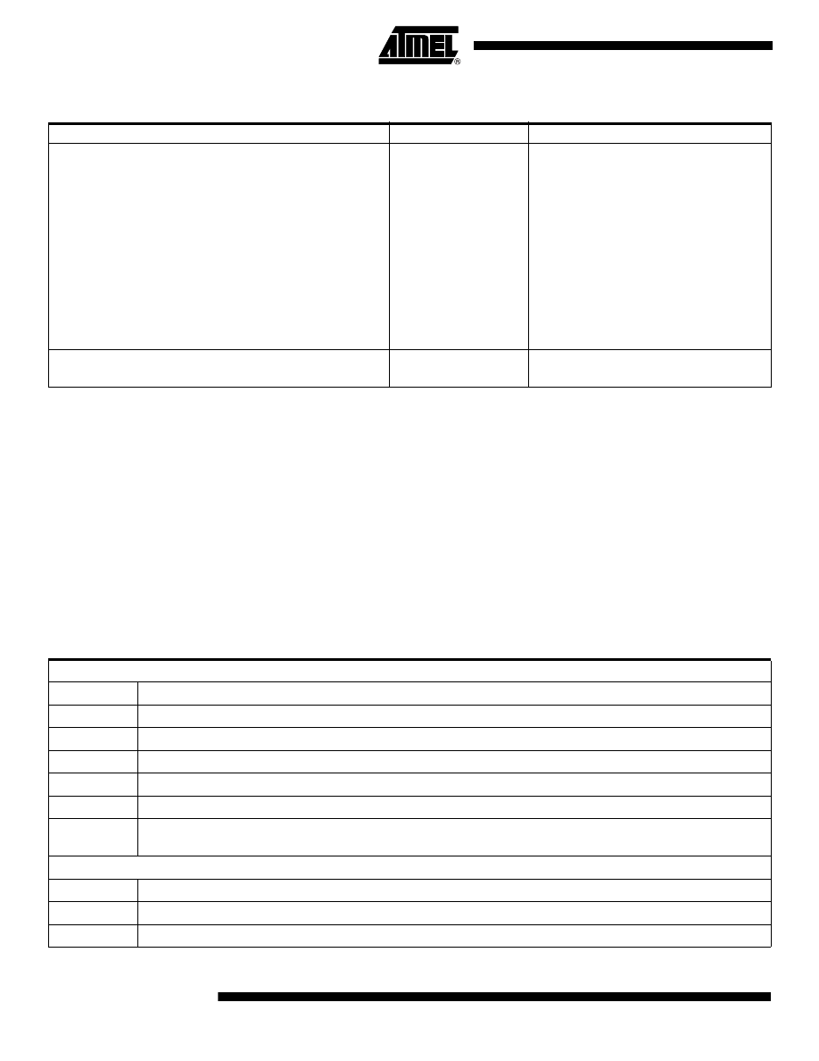
Absolute Maximum Ratings*
Operating Temperature
......................................-55 °C to +125 °C
*NOTICE:
Stresses beyond those listed under Absolute
Maximum Ratings may cause permanent dam-
age to the device. This is a stress rating only, and
functional operation of the device at these or any
other conditions beyond those indicated in the
operational sections of this specification is not
implied. Exposure to absolute maximum rating
conditions for extended periods may affect
device reliability
Storage Temperature
.........................................-65 °C to +150 °C
Voltage on Any Pin
with Respect to Ground
........................................ -1.0V to +7.0V
Maximum Operating Voltage .......................................... 6.25V
DC Output Current........................................................ 5.0 mA
3
AT93C46
5140B-SEEPR-2/07
Note:
1. This parameter is characterized and is not 100% tested.
Note:
1. V
IL
min and V
IH
max are reference only and are not tested.
Table 2. Pin Ca
Applicable over recommended operating range from T
A
= 25
°C, f = 1.0 MHz, V
CC
= +5.0V (unless otherwise noted)
Symbol
Test Conditions
Max
Units
Conditions
C
OUT
Output Capacitance (DO)
5
pF
V
OUT
= 0V
C
IN
Input Capacitance (CS, SK, DI)
5
pF
V
IN
= 0V
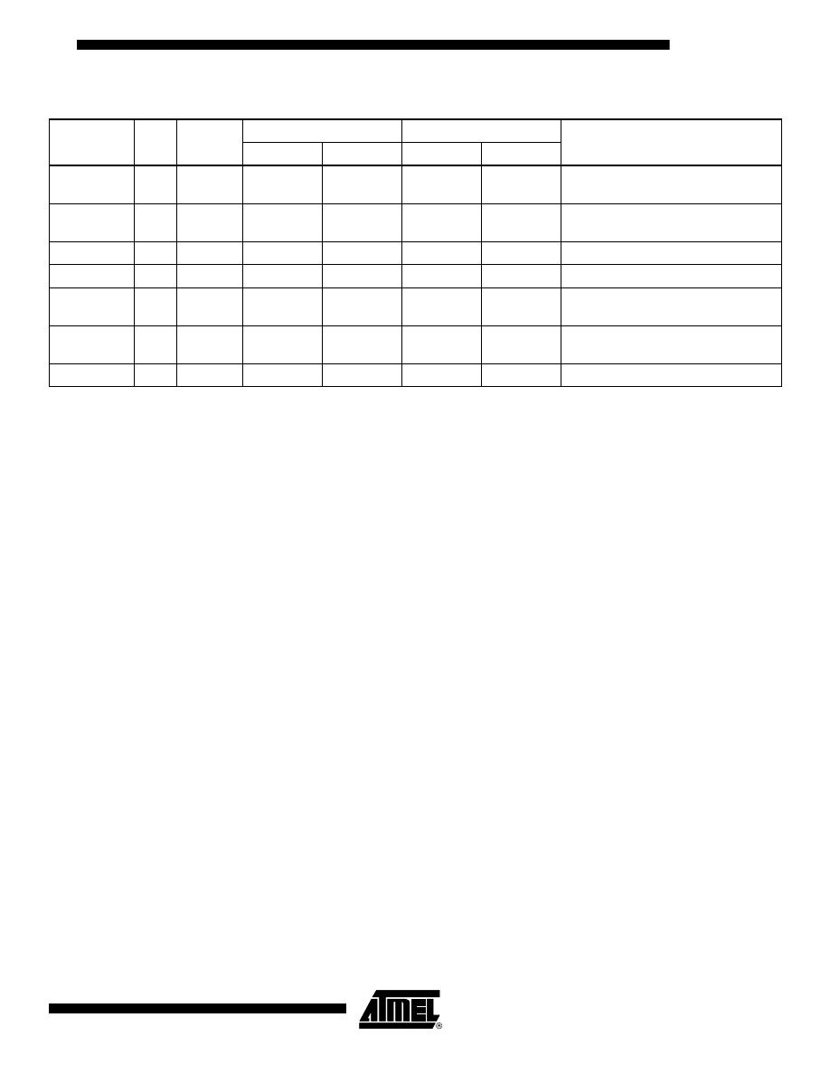
Table 3. DC Characteristics
Applicable over recommended operating range from: T
AI
=
-40 °C to +85 °C, V
CC
= +1.8V to +5.5V,
T
AE
= -40
°C to +125 °C, V
CC
= +1.8V to +5.5V (unless otherwise noted)
Symbol
Parameter
Test Condition
Min
Typ
Max
Unit
V
CC1
Supply Voltage
1.8
5.5
V
V
CC2
Supply Voltage
2.7
5.5
V
V
CC3
Supply Voltage
4.5
5.5
V
I
CC
Supply Current
V
CC
= 5.0V
READ at 1.0 MHz
0.5
2.0
mA
WRITE at 1.0 MHz
0.5
2.0
mA
I
SB1
Standby Current
V
CC
= 1.8V
CS = 0V
0
0.1
µA
I
SB2
Standby Current
V
CC
= 2.7V
CS = 0V
6.0
10.0
µA
I
SB3
Standby Current
V
CC
= 5.0V
CS = 0V
17
30
µA
I
IL
Input Leakage
V
IN
= 0V to V
CC
0.1
1.0
µA
I
OL
Output Leakage
V
IN
= 0V to V
CC
0.1
1.0
µA
V
Input Low Voltage
2.7V
≤ V
CC
≤ 5.5V
-
0.6
0.8
V
V
IH1
Input High Voltage
2.0
V
CC
+ 1
V
Input Low Voltage
1.8V
≤ V
CC
≤ 2.7V
-
0.6
V
CC
x 0.3
V
V
IH2
Input High Voltage
V
CC
x 0.7
V
CC
+ 1
V
OL1
Output Low Voltage
2.7V
≤ V
CC
≤ 5.5V
I
OL
= 2.1 mA
0.4
V
V
OH1
Output High Voltage
I
OH
=
-
0.4 mA
2.4
V
V
OL2
Output Low Voltage
1.8V
≤ V
CC
≤ 2.7V
I
OL
= 0.15 mA
0.2
V
V
OH2
Output High Voltage
I
OH
=
-
100 µA
V
CC
- 0.2
V
4
AT93C46
5140B-SEEPR-2/07
Note:
1. This parameter is characterized and is not 100% tested.
Table 4. AC Characteristics
Applicable over recommended operating range from T
AI
=
-40 °C to + 85 °C, V
CC
= As Specified,
CL = 1 TTL Gate and 100 pF (unless otherwise noted)
Symbol
Parameter
Test Condition
Min
Typ
Max
Units
f
SK
SK Clock
Frequency
4.5V
≤ V
CC
≤ 5.5V
2.7V
≤ V
CC
≤ 5.5V
1.8V
≤ V
CC
≤ 5.5V
0
0
0
2
1
0.25
MHz
t
SKH
SK High Time
4.5V
≤ V
CC
≤ 5.5V
2.7V
≤ V
CC
≤ 5.5V
1.8V
≤ V
CC
≤ 5.5V
250
250
1000
ns
t
SKL
SK Low Time
4.5V
≤ V
CC
≤ 5.5V
2.7V
≤ V
CC
≤ 5.5V
1.8V
≤ V
CC
≤ 5.5V
250
250
1000
ns
t
CS
Minimum CS
Low Time
4.5V
≤ V
CC
≤ 5.5V
2.7V
≤ V
CC
≤ 5.5V
1.8V
≤ V
CC
≤ 5.5V
250
250
1000
ns
t
CSS
CS Setup Time
Relative to SK
4.5V
≤ V
CC
≤ 5.5V
2.7V
≤ V
CC
≤ 5.5V
1.8V
≤ V
CC
≤ 5.5V
50
50
200
ns
t
DIS
DI Setup Time
Relative to SK
4.5V
≤ V
CC
≤ 5.5V
2.7V
≤ V
CC
≤ 5.5V
1.8V
≤ V
CC
≤ 5.5V
100
100
400
ns
t
CSH
CS Hold Time
Relative to SK
0
ns
t
DIH
DI Hold Time
Relative to SK
4.5V
≤ V
CC
≤ 5.5V
2.7V
≤ V
CC
≤ 5.5V
1.8V
≤ V
CC
≤ 5.5V
100
100
400
ns
t
PD1
Output Delay to
1
AC Test
4.5V
≤ V
CC
≤ 5.5V
2.7V
≤ V
CC
≤ 5.5V
1.8V
≤ V
CC
≤ 5.5V
250
250
1000
ns
t
PD0
Output Delay to
0
AC Test
4.5V
≤ V
CC
≤ 5.5V
2.7V
≤ V
CC
≤ 5.5V
1.8V
≤ V
CC
≤ 5.5V
250
250
1000
ns
t
SV
CS to Status
Valid
AC Test
4.5V
≤ V
CC
≤ 5.5V
2.7V
≤ V
CC
≤ 5.5V
1.8V
≤ V
CC
≤ 5.5V
250
250
1000
ns
t
DF
CS to DO in High
Impedance
AC Test
CS = V
IL
4.5V
≤ V
CC
≤ 5.5V
2.7V
≤ V
CC
≤ 5.5V
1.8V
≤ V
CC
≤ 5.5V
100
100
400
ns
t
WP
Write Cycle Time
10
ms
4.5V
≤ V
CC
≤ 5.5V
0.1
3
ms
Endu
5.0V, 25 °C
1M
Write Cycles
5
AT93C46
5140B-SEEPR-2/07
Note:
The Xs in the address field represent DONT CARE values and must be clocked.
Functional
Description
The AT93C46 is accessed via a simple and versatile three-wire serial communication
interface. Device operation is controlled by seven instructions issued by the host pro-
cessor. A valid instruction starts with a rising edge of CS and consists of a start bit (logic
1) followed by the appropriate op code and the desired memory address location.
READ (READ): The Read (READ) instruction contains the address code for the mem-
ory location to be read. After the instruction and address are decoded, data from the
selected memory location is available at the serial output pin DO. Output data changes
are synchronized with the rising edges of serial clock SK. It should be noted that a
dummy bit (logic 0) precedes the 8- or 16-bit data output string.
ERASE/WRITE ENABLE (EWEN): To assure data integrity, the part automatically goes
into the Erase/Write Disable (EWDS) state when power is first applied. An Erase/Write
Enable (EWEN) instruction must be executed first before any programming instructions
can be carried out. Please note that once in the EWEN state, programming remains
enabled until an EWDS instruction is executed or V
CC
power is removed from the part.
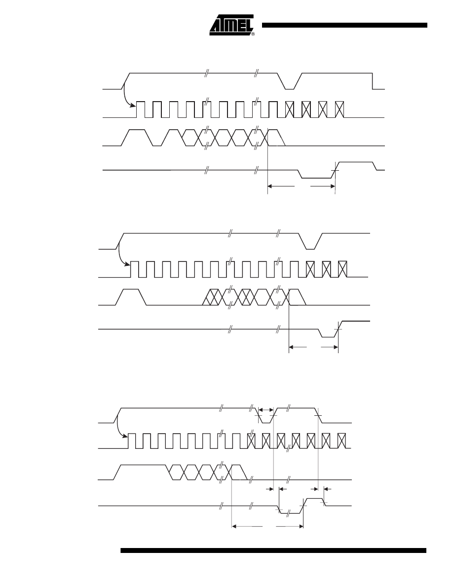
ERASE (ERASE): The Erase (ERASE) instruction programs all bits in the specified
memory location to the logical 1 state. The self-timed erase cycle starts once the
Erase instruction and address are decoded. The DO pin outputs the Ready/Busy status
of the part if CS is brought high after being kept low for a minimum of 250 ns (t
CS
). A
logic 1 at pin DO indicates that the selected memory location has been erased and the
part is ready for another instruction.
WRITE (WRITE): The Write (WRITE) instruction contains the 8 or 16 bits of data to be
written into the specified memory location. The self-timed programming cycle t
WP
starts
after the last bit of data is received at serial data input pin DI. The DO pin outputs the
Read/Busy status of the part if CS is brought high after being kept low for a minimum of
250 ns (t
CS
). A logic 0 at DO indicates that programming is still in progress. A logic 1
indicates that the memory location at the specified address has been written with the
data pattern contained in the instruction and the part is ready for further instructions. A
Ready/Busy status cannot be obtained if the CS is brought high after the end of the self-
timed programming cycle tWP.
Table 5. Instruction Set for the AT93C46
Instruction
SB
Op
Code
Address
Data
Comments
x 8
x 16
x 8
x 16
READ
1
10
A
6
- A
0
A
5
- A
0
Reads data stored in memory, at
specified address
EWEN
1
00
11XXXXX
11XXXX
Write enable must precede all
programming modes
ERASE
1
11
A
6
- A
0
A
5
- A
0
Erases memory location A
n
- A
0
WRITE
1
01
A
6
- A
0
A
5
- A
0
D
7
- D
0
D
15
- D
0
Writes memory location A
n
-
A
0
ERAL
1
00
10XXXXX
10XXXX
Erases all memory locations. Valid
only at V
CC
= 4.5V to 5.5V
WRAL
1
00
01XXXXX
01XXXX
D
7
- D
0
D
15
- D
0
Writes all memory locations. Valid
only at V
CC
= 4.5V to 5.5V
EWDS
1
00
00XXXXX
00XXXX
Disables all programming instructions
6
AT93C46
5140B-SEEPR-2/07
ERASE ALL (ERAL): The Erase All (ERAL) instruction programs every bit in the mem-
ory array to the logic 1 state and is primarily used for testing purposes. The DO pin
outputs the Ready/Busy status of the part if CS is brought high after being kept low for a
minimum of 250 ns (t
CS
). The ERAL instruction is valid only at V
CC
= 5.0V
± 10%.
WRITE ALL (WRAL): The Write All (WRAL) instruction programs all memory locations
with the data patterns specified in the instruction. The DO pin outputs the Ready/Busy
status of the part if CS is brought high after being kept low for a minimum of 250 ns (t
CS
).
The WRAL instruction is valid only at V
CC
= 5.0V ±
10%.
ERASE/WRITE DISABLE (EWDS): To protect against accidental data disturb, the
Erase/Write Disable (EWDS) instruction disables all programming modes and should be
executed after all programming operations. The operation of the Read instruction is
independent of both the EWEN and EWDS instructions and can be executed at any
time.
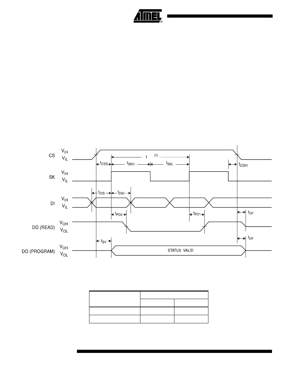
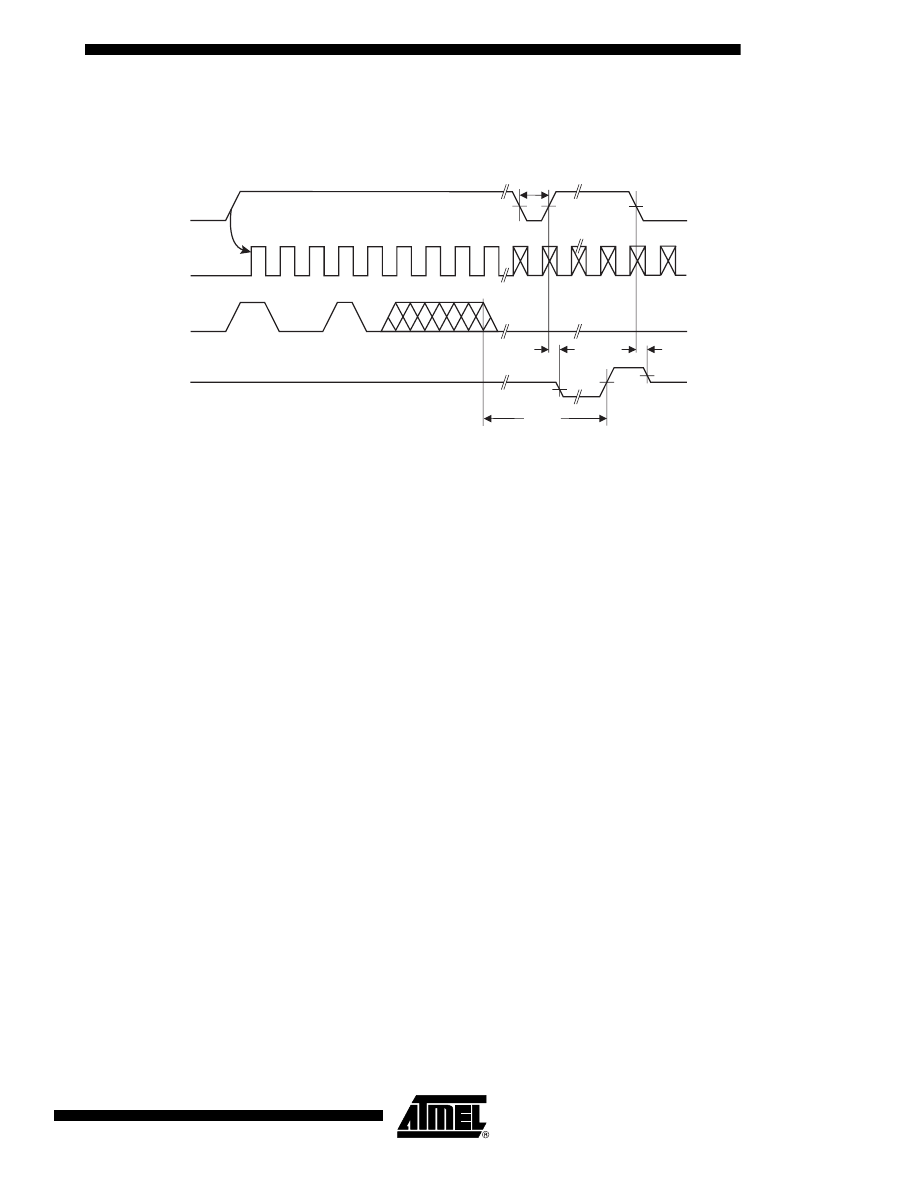
Timing Diagrams
Figure 2. Synchronous Data Timing
Note:
1. This is the minimum SK period.
µs
Table 6. Organization Key for Timing Diagrams
I/O
AT93C46 (1K)
x 8
x 16
A
N
A
6
A
5
D
N
D
7
D
15
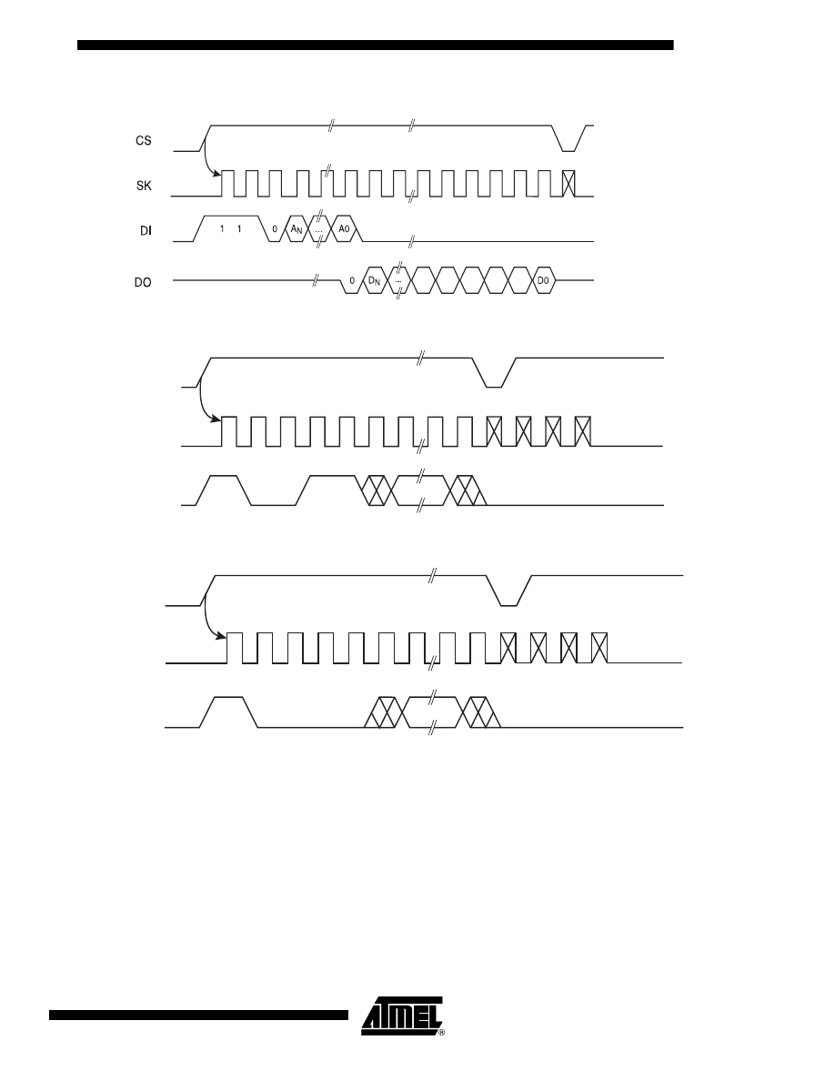
7
AT93C46
5140B-SEEPR-2/07
Figure 3. READ Timing
Figure 4. EWEN Timing
Figure 5. EWDS Timing
High Impedance
t
CS
CS
1
1
...
0
0
1
SK
DI
t
CS
CS
t
CS
SK
DI
1
0
0
0
0
...
8
AT93C46
5140B-SEEPR-2/07
Figure 6. WRITE Timing
Figure 7.
Note:
1. Valid only at V
CC
= 4.5V to 5.5V.
Figure 8. ERASE Timing
SK
CS
t
CS
t
WP
1
1
A
N
D
N
0
A0
D0
...
...
DI
DO
HIGH IMPEDANCE
BUSY
READY
CS
SK
DI
DO
HIGH IMPEDANCE
BUSY
READY
1
0
0
1
...
D
N
t
CS
t
WP
...
D0
0
SK
1
1
...
1
CS
DI
A
N
t
CS
t
SV
t
DF
t
WP
A
N-1
A
N-2
A0
CHECK
STATUS
STANDBY
READY
BUSY
DO
HIGH IMPEDANCE
HIGH IMPEDANCE
9
AT93C46
5140B-SEEPR-2/07
Figure 9. ERAL Timing
Note:
1. Valid only at V
CC
= 4.5V to 5.5V.
SK
CS
DI
1
1
0
0
0
DO
HIGH IMPEDANCE
HIGH IMPEDANCE
READY
BUSY
CHECK
STATUS
STANDBY
t
WP
t
CS
t
SV
t
DF
10
AT93C46
5140B-SEEPR-2/07
Notes: 1. For 2.7V devices used in the 4.5V to 5.5V range, please refer to performance values in th
Not recommended for new design. Please refer to AT93C46D datasheet.
2. U designates Green Package and RoHS compliant.
3. H designates Green Package and RoHS compliant, with NiPdAu Lead finish
4. Available in waffle pack and wafer form, order as SL788 for inkless wafer form. Bumped die available upon request.
AT93C46 Ordering Information
(1)
Ordering Code
Package
Operation Range
AT93C46-10PU-2.7
(2)
AT93C46-10PU-1.8
(2)
AT93C46-10SU-2.7
(2)
AT93C46-10SU-1.8
(2)
AT93C46W-10SU-2.7
(2)
AT93C46W-10SU-1.8
(2)
AT93C46-10TU-2.7
(2)
AT93C46-10TU-1.8
(2)
AT93C46Y1-10YU-1.8
(2)
(Not recommended for new
designs)
AT93C46Y6-10YH-1.8
(3)
AT93C46U3-10UU-1.8
(2)
8P3
8P3
8S1
8S1
8S2
8S2
8A2
8A2
8Y1
8Y6
8U3-1
Lead-free/Halogen-free/
Industrial Temperature
(
-40 °C to 85 °C)
AT93C46-W1.8-11
(4)
Die Sale
Industrial
(
-40 °C to 85 °C)
Package Type
8P3
8-lead, 0.300" Wide, Plastic Dual Inline Package (PDIP)
8S1
8-lead, 0.150" Wide, Plastic Gull Wing Small Outline (JEDEC SOIC)
8S2
8-lead, 0.200" Wide, Plastic Gull Wing Small Outline (EIAJ SOIC)
8A2
8-lead, 0.170" Wide, Thin Shrink Small Outline Package (TSSOP)
8U3-1
8-ball, Die Ball Grid Array Package (dBGA2)
8Y1
8-lead, 4.90 mm x 3.00 mm Body, Dual Footprint, Non-leaded, Miniature Array Package (MAP)
8Y6
8-lead, 2.00 mm x 3.00 mm Body, 0.50mm Pitch, Ultra-Thin Mini-MAO, Dual No Lead Package. (DFN), (MLP
2x3mm)
Options
-2.7
Low Voltage (2.7V to 5.5V)
-1.8
Low Voltage (1.8V to 5.5V)
R
Rotated Pinout
11
AT93C46
5140B-SEEPR-2/07
Packaging Information
8P3 - PDIP
2325 Orchard Parkway
San Jose, CA 95131
TITLE
DRAWING NO.
R
REV.
8P3, 8-lead, 0.300" Wide Body, Plastic Dual
In-line Package (PDIP)
01/09/02
8P3
B
D
D1
E
E1
e
L
b2
b
A2 A
1
N
eA
c
b3
4 PLCS
Top View
Side View
End View
COMMON DIMENSIONS
(Unit of Measure = inches)
SYMBOL
MIN
NOM
MAX
NOTE
Notes:
1. This drawing is for general information only; refer to JEDEC Drawing MS-001, Variation BA for additional information.
2. Dimensions A and L are measured with the package seated in JEDEC seating plane Gauge GS-3.
3. D, D1 and E1 dimensions do not include mold Flash or protrusions. Mold Flash or protrusions shall not exceed 0.010 inch.
4. E and eA measured with the leads constrained to be perpendicular to datum.
5. Pointed or rounded lead tips are preferred to ease insertion.
6. b2 and b3 maximum dimensions do not include Dambar protrusions. Dambar protrusions shall not exceed 0.010 (0.25 mm).
A
0.210
2
A2
0.115
0.130
0.195
b
0.014
0.018
0.022
5
b2
0.045
0.060
0.070
6
b3
0.030
0.039
0.045
6
c
0.008
0.010
0.014
D
0.355
0.365
0.400
3
D1
0.005
3
E
0.300
0.310
0.325
4
E1
0.240
0.250
0.280
3
e
0.100 BSC
eA
0.300 BSC
4
L
0.115
0.130
0.150
2
12
AT93C46
5140B-SEEPR-2/07
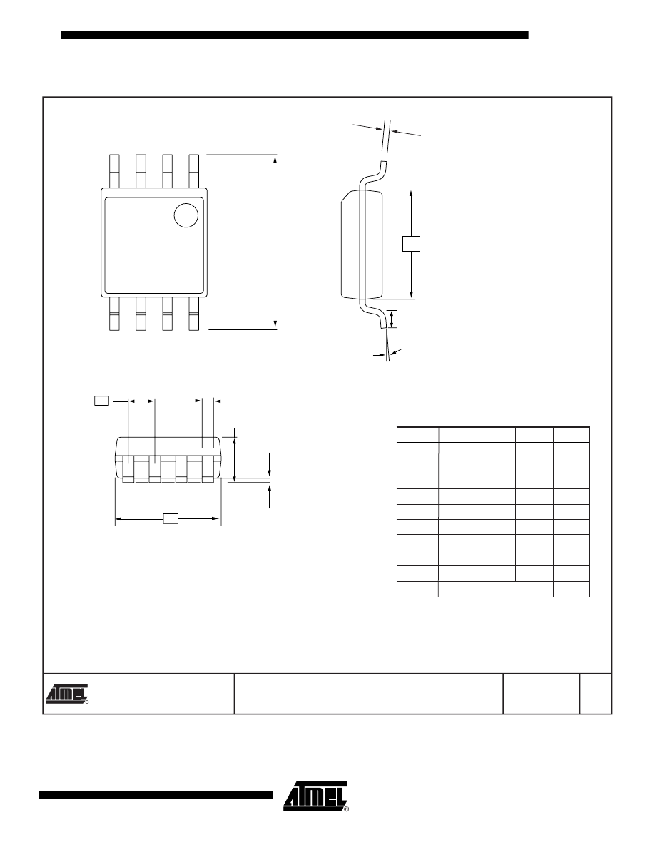
8S1 - JEDEC SOIC
1150 E. Cheyenne Mtn. Blvd.
Colorado Springs, CO 80906
TITLE
DRAWING NO.
R
REV.
Note:
10/7/03
8S1, 8-lead (0.150" Wide Body), Plastic Gull Wing
Small Outline (JEDEC SOIC)
8S1
B
COMMON DIMENSIONS
(Unit of Measure = mm)
SYMBOL
MIN
NOM
MAX
NOTE
A1
0.10
-
0.25
These drawings are for general information only. Refer to JEDEC Drawing MS-012, Variation AA for proper dimensions, tolerances, datums, etc.
A
1.35
-
1.75
b
0.31
-
0.51
C
0.17
-
0.25
D
4.80
-
5.00
E1
3.81
-
3.99
E
5.79
-
6.20
e
1.27 BSC
L
0.40
-
1.27
0°
-
8°
Top View
End View
Side View
e
B
D
A
A1
N
E
1
C
E1
L
13
AT93C46
5140B-SEEPR-2/07
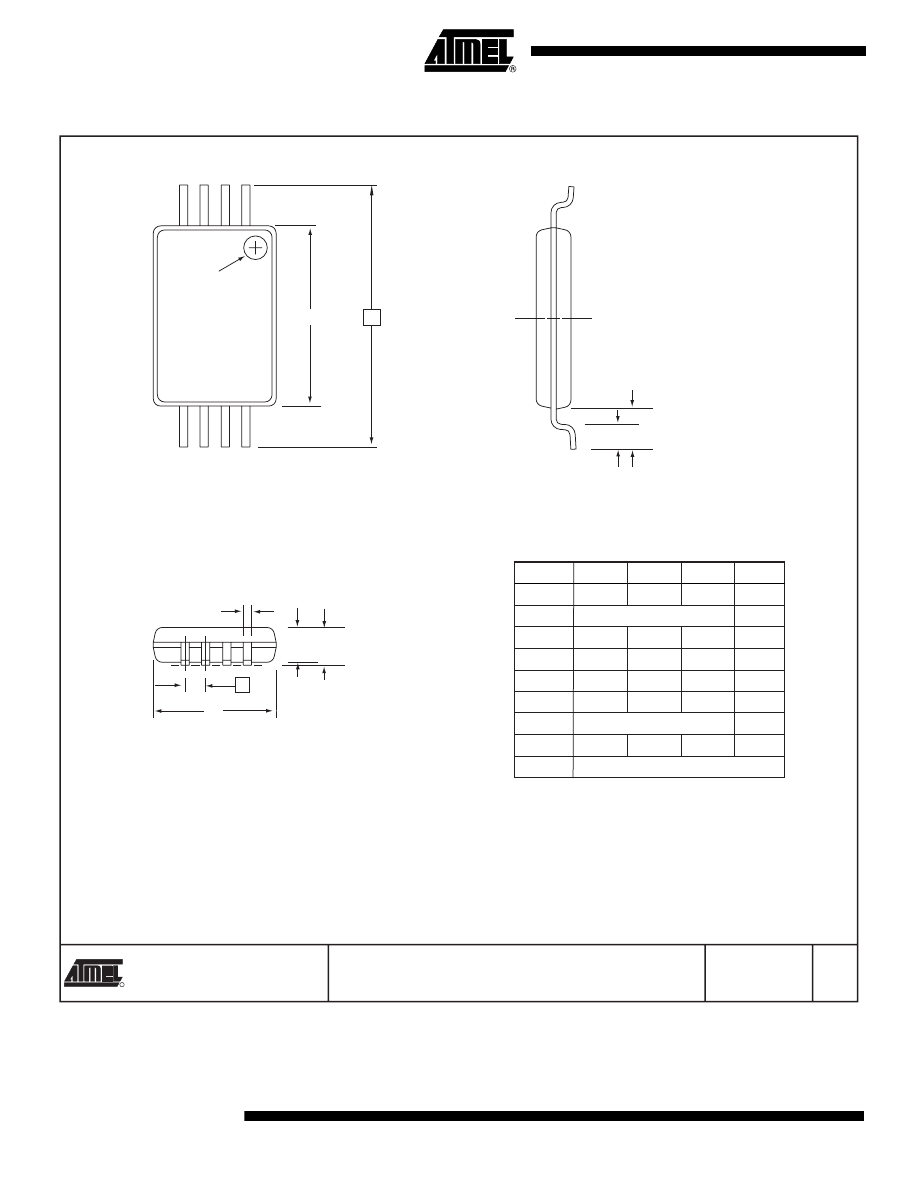
8S2 - EIAJ SOIC
2325 Orchard Parkway
San Jose, CA 95131
TITLE
DRAWING NO.
R
REV.
8S2, 8-lead, 0.209" Body, Plastic Small
Outline Package (EIAJ)
10/7/03
8S2
C
COMMON DIMENSIONS
(Unit of Measure = mm)
SYMBOL
MIN
NOM
MAX
NOTE
Notes: 1. This drawing is for general information only; refer to EIAJ Drawing EDR-7320 for additional information.
2. Mismatch of the upper and lower dies and resin burrs are not included.
3. It is recommended that upper and lower cavities be equal. If they are different, the larger dimension shall be regarded.
4. Determines the true geometric position.
5. Values b and C apply to pb/Sn solder plated terminal. The standard thickness of the solder layer shall be 0.010 +0.010/
-
0.005 mm.
A
1.70
2.16
A1
0.05
0.25
b
0.35
0.48
5
C
0.15
0.35
5
D
5.13
5.35
E1
5.18
5.40
2, 3
E
7.70
8.26
L
0.51
0.85
0°
8°
e
1.27 BSC
4
End View
Side View
e
b
A
A1
D
E
N
1
C
E1
L
Top View
14
AT93C46
5140B-SEEPR-2/07
8A2 - TSSOP
2325 Orchard Parkway
San Jose, CA 95131
TITLE
DRAWING NO.
R
REV.
5/30/02
COMMON DIMENSIONS
(Unit of Measure = mm)
SYMBOL
MIN
NOM
MAX
NOTE
D
2.90
3.00
3.10
2, 5
E
6.40 BSC
E1
4.30
4.40
4.50
3, 5
A
-
-
1.20
A2
0.80
1.00
1.05
b
0.19
-
0.30
4
e
0.65 BSC
L
0.45
0.60
0.75
L1
1.00 REF
8A2, 8-lead, 4.4 mm Body, Plastic
Thin Shrink Small Outline Package (TSSOP)
Notes:
1. This drawing is for general information only. Refer to JEDEC Drawing MO-153, Variation AA, for proper dimensions, tolerances,
datums, etc.
2. Dimension D does not include mold Flash, protrusions or gate burrs. Mold Flash, protrusions and gate burrs shall not exceed
0.15 mm (0.006 in) per side.
3. Dimension E1 does not include inter-lead Flash or protrusions. Inter-lead Flash and protrusions shall not exceed 0.25 mm
(0.010 in) per side.
4. Dimension b does not include Dambar protrusion. Allowable Dambar protrusion shall be 0.08 mm total in excess of the
b dimension at maximum material condition. Dambar cannot be located on the lower radius of the foot. Minimum space between
protrusion and adjacent lead is 0.07 mm.
5. Dimension D and E1 to be determined at Datum Plane H.
8A2
B
Side View
End View
Top View
A2
A
L
L1
D
1
2
3
E1
N
b
Pin 1 indicator
this corner
E
e
15
AT93C46
5140B-SEEPR-2/07
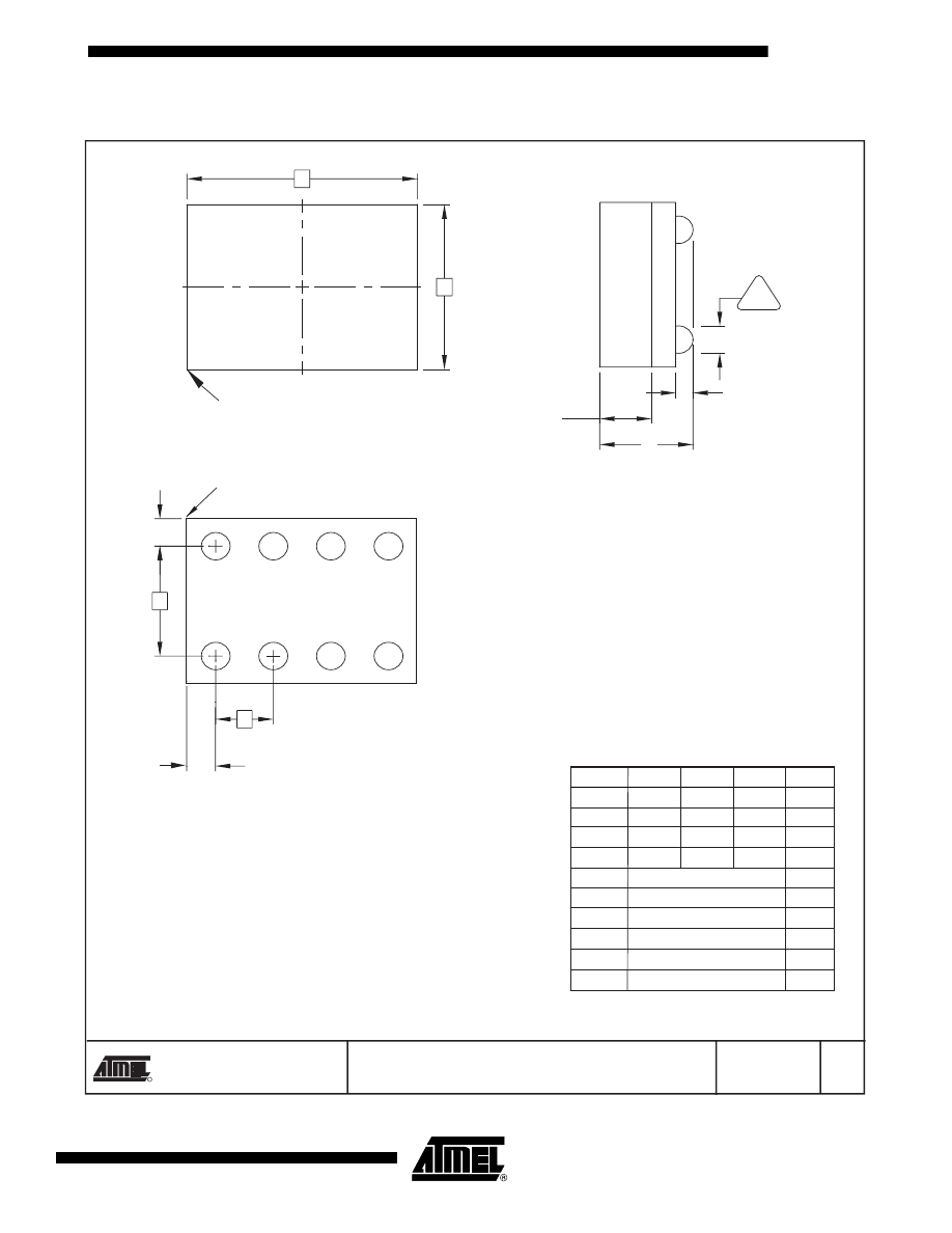
8U3-1 - dBGA2
1150 E. Cheyenne Mtn. Blvd.
Color
a
do
S
pring
s
, CO
8
0906
TITLE
DRAWING NO.
R
REV.
PO
8
U
3
-1 A
6/24/0
3
COMMON DIMENSIONS
(Unit of Me
asu
re = mm)
SYMBOL
MIN
NOM
MAX
NOTE
8U3-1,
8
-
ba
ll, 1.50 x 2.00 mm Body, 0.50 mm pitch,
S
m
a
ll Die B
a
ll Grid Arr
a
y P
a
ck
a
ge (dBGA2)
A 0.71
0.
8
1 0.91
A1 0.10
0.15
0.20
A2 0.40
0.45
0.50
b
0.20
0.25
0.
3
0
D
1.50 B
S
C
E
2.00 B
S
C
e
0.50 B
S
C
e1
0.25 REF
d
1.00 B
S
C
d1
0.25 REF
1. Dimen
s
ion
b
i
s
me
asu
red
a
t the m
a
xim
u
m
s
older
ba
ll di
a
meter.
Thi
s
dr
a
wing i
s
for gener
a
l inform
a
tion only.
Bottom View
8
S
OLDER BALL
S
b
D
E
Top View
PIN 1 BALL PAD CORNER
A
S
ide View
A
2
A
1
4
5
PIN 1 BALL PAD CORNER
3
1
e
2
6
7
8
d
(e1)
(d1)
1.
16
AT93C46
5140B-SEEPR-2/07
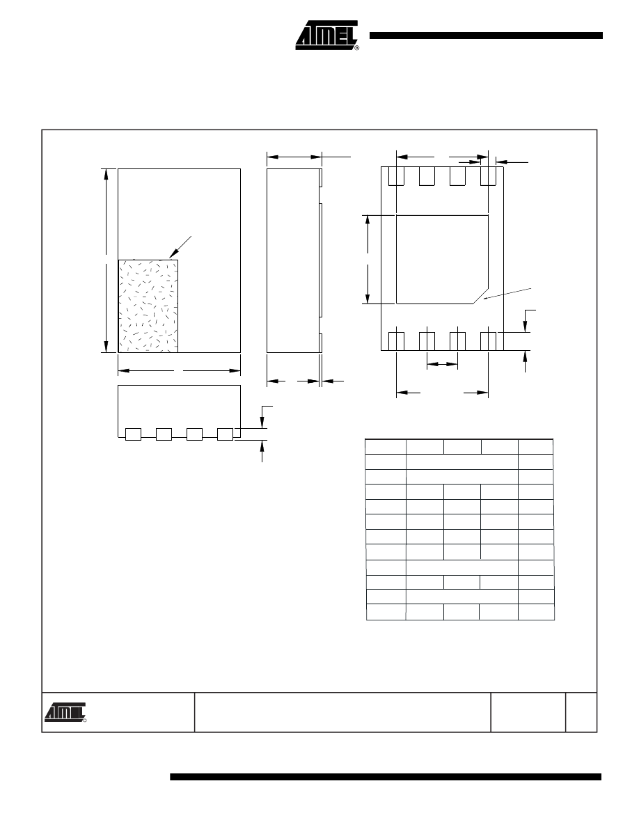
8Y6 - Mini-MAP
2325 Orchard Parkway
San Jose, CA 95131
TITLE
DRAWING NO.
R
REV.
8Y6, 8-lead 2.0 x 3.0 mm Body, 0.50 mm Pitch, Utlra Thin Mini-Map,
Dual No Lead Package (DFN) ,(MLP 2x3)
C
8Y6
8/26/05
Notes:
1. This drawing is for general information only. Refer to JEDEC Drawing MO-229, for proper dimensions,
tolerances, datums, etc.
2. Dimension b applies to metallized terminal and is measured between 0.15 mm and 0.30 mm from the terminal tip. If the
terminal has the optional radius on the other end of the terminal, the dimension should not be measured in that radius area.
COMMON DIMENSIONS
(Unit of Measure = mm)
SYMBOL
MIN
NOM
MAX
NOTE
D
2.00 BSC
E
3.00 BSC
D2
1.40
1.50
1.60
E2
-
-
1.40
A
-
-
0.60
A1
0.0
0.02
0.05
A2
-
-
0.55
A3
0.20 REF
L
0.20
0.30
0.40
e
0.50 BSC
b
0.20
0.25
0.30
2
A2
b
(8X)
Pin 1 ID
Pin 1
Index
Area
A1
A3
D
E
A
L (8X)
e (6X)
1.50 REF.
D2
E2
17
AT93C46
5140B-SEEPR-2/07
Revision History
Doc. Rev.
Date
Comments
5140B
2/2007
Implemented revision history.
Added note to page 1 and ordering information; Not
recommended for new design; please refer to AT93C46D
datasheet.

Printed on recycled paper.
5140B-SEEPR-2/07
Disclaimer: The information in this document is provided in connection with Atmel products. No license, express or implied, by estoppel or otherwise, to any
intellectual property right is granted by this document or in connection with the sale of Atmel products. EXCEPT AS SET FORTH IN ATMELS TERMS AND CONDI-
TIONS OF SALE LOCATED ON ATMELS WEB SITE, ATMEL ASSUMES NO LIABILITY WHATSOEVER AND DISCLAIMS ANY EXPRESS, IMPLIED OR STATUTORY
WARRANTY RELATING TO ITS PRODUCTS INCLUDING, BUT NOT LIMITED TO, THE IMPLIED WARRANTY OF MERCHANTABILITY, FITNESS FOR A PARTICULAR
PURPOSE, OR NON-INFRINGEMENT. IN NO EVENT SHALL ATMEL BE LIABLE FOR ANY DIRECT, INDIRECT, CONSEQUENTIAL, PUNITIVE, SPECIAL OR INCIDEN-
TAL DAMAGES (INCLUDING, WITHOUT LIMITATION, DAMAGES FOR LOSS OF PROFITS, BUSINESS INTERRUPTION, OR LOSS OF INFORMATION) ARISING OUT
OF THE USE OR INABILITY TO USE THIS DOCUMENT, EVEN IF ATMEL HAS BEEN ADVISED OF THE POSSIBILITY OF SUCH DAMAGES. Atmel makes no
representations or warranties with respect to the accuracy or completeness of the contents of this document and reserves the right to make changes to specifications
and product descriptions at any time without notice. Atmel does not make any commitment to update the information contained herein. Unless specifically provided
otherwise, Atmel products are not suitable for, and shall not be used in, automotive applications. Atmels products are not intended, authorized, or warranted for use
as components in applications intended to support or sustain life
Atmel Corporation
Atmel Operations
2325 Orchard Parkway
San Jose, CA 95131, USA
Tel: 1(408) 441-0311
Fax: 1(408) 487-2600
Regional Headquarters
Europe
Atmel Sarl
Route des Arsenaux 41
Case Postale 80
CH-1705 Fribourg
Switzerland
Tel: (41) 26-426-5555
Fax: (41) 26-426-5500
Asia
Room 1219
Chinachem Golden Plaza
77 Mody Road Tsimshatsui
East Kowloon
Hong Kong
Tel: (852) 2721-9778
Fax: (852) 2722-1369
Japan
9F, Tonetsu Shinkawa Bldg.
1-24-8 Shinkawa
Chuo-ku, Tokyo 104-0033
Japan
Tel: (81) 3-3523-3551
Fax: (81) 3-3523-7581
Memory
2325 Orchard Parkway
San Jose, CA 95131, USA
Tel: 1(408) 441-0311
Fax: 1(408) 436-4314
Microcontrollers
2325 Orchard Parkway
San Jose, CA 95131, USA
Tel: 1(408) 441-0311
Fax: 1(408) 436-4314
La Chantrerie
BP 70602
44306 Nantes Cedex 3, France
Tel: (33) 2-40-18-18-18
Fax: (33) 2-40-18-19-60
ASIC/ASSP/Smart Cards
Zone Industrielle
13106 Rousset Cedex, France
Tel: (33) 4-42-53-60-00
Fax: (33) 4-42-53-60-01
1150 East Cheyenne Mtn. Blvd.
Colorado Springs, CO 80906, USA
Tel: 1(719) 576-3300
Fax: 1(719) 540-1759
Scottish Enterprise Technology Park
Maxwell Building
East Kilbride G75 0QR, Scotland
Tel: (44) 1355-803-000
Fax: (44) 1355-242-743
RF/Automotive
Theresienstrasse 2
Postfach 3535
74025 Heilbronn, Germany
Tel: (49) 71-31-67-0
Fax: (49) 71-31-67-2340
1150 East Cheyenne Mtn. Blvd.
Colorado Springs, CO 80906, USA
Tel: 1(719) 576-3300
Fax: 1(719) 540-1759
Biometrics/Imaging/Hi-Rel MPU/
High Speed Converters/RF Datacom
Avenue de Rochepleine
BP 123
38521 Saint-Egreve Cedex, France
Tel: (33) 4-76-58-30-00
Fax: (33) 4-76-58-34-80
Literature Requests
www.atmel.com/literature
© 2007 Atmel Corporation. All rights reserved. Atmel
®
, logo and combinations thereof, Everywhere You Are
®
and others, are registered
trademarks or trademarks of Atmel Corporation or its subsidiaries. Other terms and product names may be trademarks of others.
Document Outline
-
- 8Y1 - MAP