| Secciones |
|---|
| Foros Electrónica |
|
|
| Boletines de correo |
 |

General Description
The MAX14748 USB battery charger integrates a charger
detector, boost/buck converter, and Li+ battery charger
with smart power selector to provide fast and safe charging
of 2s Li+ battery packs.
The MAX14748 provides support for devices functioning
as a UFP/DRP per the USB Type-C 1.1 standard, while
also providing detection of legacy USB Battery Charging
Specification, Revision 1.2 (BC1.2) compliant chargers in
addition to other nonstandard chargers. The programmable
Automatic Input Current Limiting (AICL) feature ensures that
maximum safe current is drawn from the charging adapter.
The Li+ charger includes an automatic Smart Power
Selector™ to simultaneously charge the battery and
provide power to the system load. The Smart Power
Selector function will supplement the system power with
the battery if power from the charging adapter is insufficient.
The Li+ charger features JEITA thermal monitoring and
charger voltage/current reduction or charger disable.
The MAX14748 is available in a 54-bump, 0.4mm pitch,
3.97mm x 2.77mm x 0.64mm wafer-level package (WLP)
and operates over the -40 °C to +85 °C extended temperature
range.
Applications
Digital Imaging (DSC, DVC)
Wireless Speakers
Handheld Barcode Readers
Benefits and Features
Minimize Power Management Footprint Through High
Integration
13mΩ (typ) Integrated Battery To System Switch
Thermal Current Limiting
DC-DC Converter with Boost and Reverse Buck
High Efficiency
- 92% in Boost Mode at 1A Output Current and
7.4V Battery Voltage
- 94% in Reverse Buck Mode at 500mA Output
Internal USB Switch for USB D+/D- Data Lines
Easy-to-Implement Li+ Battery Charging
Charges 2s Li-Ion Batteries from Legacy 5V USB
Adapters
- 15W Input Power with 3A Type-C Adapter
- 7.5W Input Power with DCP Adapter
- 1A System/Charge Current From DCP Adapter
- 2A System/Charge Current From 3A Type-C Adapter
USB Type-C Specification, Rev 1.1 Support
UFP/DRP Operation
V
CONN
and Super-Speed Multiplexer Logic Controls
Non-Standard DCP Detection
USB Battery Charging Specification, Rev 1.2 Compliant
Automatic Input Current Limit (AICL) Power
Management
Support Weak/Dead Batteries Detection
Smart Power Selector
Thermistor Monitor
Various Protection Features
28V Integrated Overvoltage Protection
JEITA Charge Protection
±15kV ESD Protection on USB Adapter Pins
19-100081; Rev 0; 6/17
Smart Power Selector is a trademark of Maxim Integrated
Products, Inc.
MAX14748
USB Type-C Charger

Voltages Referenced to GND
CHGIN ..................................................................-0.3V to +30V
BST .......................................................................-0.3V to +16V
SYS to BAT ..........................................................-0.3V to +12V
BAT, SYS ..............................................................-0.3V to +12V
BYP to CHGIN ......................................................-30V to +0.3V
BYP, THM, INT, SYSOK, FLTIN, FSUS,
LED, SDA, SCL ....................................................-0.3V to 6V
COMP, SET .......................................... -0.3V to V
CCINT
+ 0.3V
CC1, CC2, TDN, TDP, CDN, CDP, V
CONN
............-0.3V to +6V
CC1, CC2, in fault mode through a 10k resistor ..-0.3V to +20V
CDIR .......................................................................-0.3V to +6V
VTPU (VTPU-TPU switch open) .......... -0.3V to V
CCINT
+ 0.3V
TPU (VTPU-TPU switch open) .........-0.3V to 6 or VTPU + 0.3V
VTPU, TPU Maximum Current
(VTPU-TPU switch closed) ...................... -100mA to +100mA
BVCEN ..................................................-0.3V to V
CCINT
+ 0.3V
SFOUT, V
CCINT
, BREG ....... -0.3V to min ((V
CHGIN
+ 0.3), 6)V
LX .............................................................-0.3V to V
SYS
+ 0.3V
NVP ......................................................................-0.3V to +30V
AGND, DGND, PGND, GND ...............................-0.3V to +0.3V
Continuous Current into
CHGIN, SYS ...................................................................+6.4A
BAT .................................................................................+4.8A
Any Other Terminal .....................................................+100mA
Continuous Power Dissipation
(multilayer board at +70 °C): 9 x 6 Array 54-Bump,
3.97mm x 2.77mm 0.4mm Pitch WLP
(derate 24.46mW/ °C) .................................................1.957W
Operating Temperature Range .......................... -40 °C to +85 °C
Junction Temperature ................................................... +150 °C
Storage Temperature Range ........................... -65 °C to +150 °C
Lead Temperature (soldering, 10s) .............................. +300 °C
Soldering Temperature (reflow) .................................... +260 °C
WLP
Junction-to-Ambient Thermal Resistance (Θ
JA
) .....40.88 °C/W
(Note 1)
(V
BAT
= 8.3V, T
A
= -40 °C to +85 °C, all registers in their default state, unless otherwise noted. Typical values are at V
CHGIN
= 5.0V,
V
BAT
=7.4V, V
SYS
= V
BATREG
, T
A
= +25 °C.)
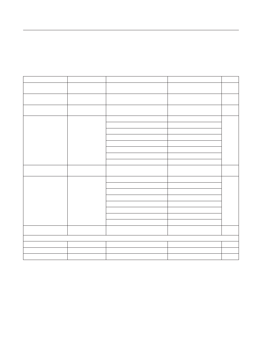
Electrical Characteristics
PARAMETER
SYMBOL
CONDITIONS
MIN
TYP
MAX
UNITS
SUPPLY CURRENT
BAT Supply Current
I
BAT
V
CHGIN
= 0V or Floating, Type-C
detection active
140
µA
Low Power mode
25
µA
CHGIN Supply Current
I
CHG
V
CHGIN
= +5V, T
A
+25 °C,
ChgEn = 0
5.3
mA
V
CHGIN
= +5V, T
A
+25 °C,
Suspend Mode (FSUS = High)
0.98
mA
CHGIN TO BYP PATH
Allowed CHGIN Input
Voltage Range
V
CHGIN_RNG
0
28
V
CHGIN Detect
Threshold
V
BDET
Rising
3.8
3.9
4.0
V
V
BDET_F
Falling
3.6
3.7
3.8
CHGIN Overvoltage
Threshold
V
OVP
Rising
5.59
5.66
5.72
V
V
OVP_F
Falling
5.56
V
V
OVP_H
Hysteresis
28
mV
MAX14748
USB Type-C Charger
www.maximintegrated.com
Maxim Integrated
2
Note 1: Package thermal resistances were obtained using the method described in JEDEC specification JESD51-7, using a four-layer
board. For detailed information on package thermal considerations, refer to
.
Absolute Maximum Ratings
Stresses beyond those listed under Absolute Maximum Ratings may cause permanent damage to the device. These are stress ratings only, and functional operation of the device at these
or any other conditions beyond those indicated in the operational sections of the specifications is not implied. Exposure to absolute maximum rating conditions for extended periods may affect
device reliability.
Package Thermal Characteristics

(V
BAT
= 8.3V, T
A
= -40 °C to +85 °C, all registers in their default state, unless otherwise noted. Typical values are at V
CHGIN
= 5.0V,
V
BAT
=7.4V, V
SYS
= V
BATREG
, T
A
= +25 °C.)
PARAMETER
SYMBOL
CONDITIONS
MIN
TYP
MAX
UNITS
CHGIN-BYP Resistance
R
CHGIN_BYP
V
CHGIN
= 5V
45
mW
CHGIN-BYP Soft-Start
Timeout
t
BYP_SFTTO
If V
BYP
has not reached within
50mV of V
CHGIN
at timeout, a fault
is flagged by SysFlt of register
0x02.
100
ms
CHGIN-BYP Soft-Start
Current
I
BYP_SFT
60
mA
CHGIN-BYP Soft-Start
End Comparator
V
BYP_SFTEND
15
50
80
mV
CHGIN-BYP Overload
Comparator
V
BYP_OVL
290
360
420
mV
Input Current Limit
I
LIM
SpvChgILim[4:0] = 00100
0.4
A
SpvChgILim[4:0] = 01110
1.5
SpvChgILim[4:0] = 11101
3
Input Current Limit
Programming Range
I
LIM_RNG
0.1
3
A
Input Current Limit
Programming Step
I
LIM_STEP
100
mA
INTERNAL SUPPLIES
Internal V
CCINT
Regulator
V
CCINT
V
CHGIN
= 5V, boost off
4.0
4.3
4.6
V
Boost Regulator BREG
V
BREG
4.3
V
V
CCINT
UVLO
Threshold
V
UVLO
V
CCINT
rising
3.1
3.4
3.7
V
V
CCINT
falling
3.0
3.3
3.6
V
CCINT
UVLO
Threshold Hysteresis
V
UVLO_HYS
Hysteresis
100
mV
BAT UVLO Threshold
V
BATUVLO
Rising
4
V
BAT UVLO Hysteresis
V
BATUVLO_H
100
mV
SFOUT LDO Voltage
V
SFOUT
SfOutLvl = 1, V
CHGIN
= 6V,
I
SFOUT
= 0
3.15
3.3
3.45
V
SfOutLvl = 1, V
CHGIN
= 6V,
I
SFOUT
= 15mA
2.95
SfOutLvl = 0, V
CHGIN
= 6V,
I
SFOUT
= 0
5.0
5.25
5.5
SfOutLvl = 0, VCHGIN = 6V,
I
SFOUT
= 15mA
4.9
SFOUT Maximum
Current
I
SFOUT_MAX
15
mA
MAX14748
USB Type-C Charger
www.maximintegrated.com
Maxim Integrated
3
Electrical Characteristics (continued)
(V
BAT
= 8.3V, T
A
= -40 °C to +85 °C, all registers in their default state, unless otherwise noted. Typical values are at V
CHGIN
= 5.0V,
V
BAT
=7.4V, V
SYS
= V
BATREG
, T
A
= +25 °C.)
PARAMETER
SYMBOL
CONDITIONS
MIN
TYP
MAX
UNITS
Current Reduce
Temperature
T
CHG_LIM
120
°C
Thermal Shutdown
Temperature
T
SHUTDOWN
150
°C
Thermal Shutdown
Hysteresis
T
SHUTDOWN_H
20
°C
BYP UVLO Threshold
V
BYPUVLO
BYPUVLO[2:0] = 000, V
BYP
falling
3.8
V
BYPUVLO[2:0] = 001, V
BYP
falling
3.9
BYPUVLO[2:0] = 010, V
BYP
falling
4.0
BYPUVLO[2:0] = 011, V
BYP
falling
4.1
BYPUVLO[2:0] = 100, V
BYP
falling
4.2
BYPUVLO[2:0] = 101, V
BYP
falling
4.3
BYPUVLO[2:0] = 110, V
BYP
falling
4.4
BYPUVLO[2:0] = 111, V
BYP
falling
4.5
BYP UVLO Threshold
Hysteresis
V
BYPUVLO_H
25
mV
SYS UVLO (SYSOK)
Threshold
V
SYSUVLO
VPChg[2:0] = 000, V
SYS
rising
5.9
V
VPChg[2:0] = 001, V
SYS
rising
6.0
VPChg[2:0] = 010, V
SYS
rising
6.1
VPChg[2:0] = 011, V
SYS
rising
6.2
VPChg[2:0] = 100, V
SYS
rising
6.3
VPChg[2:0] = 101, V
SYS
rising
6.4
VPChg[2:0] = 110, V
SYS
rising
6.5
VPChg[2:0] = 111, V
SYS
rising
6.6
SYS UVLO Threshold
Hysteresis
V
SYSUVLO_H
500
mV
BYP-SYS BOOST PATH
Switching Frequency
f
BST_SW
0.8
MHz
Maximum Input Current
I
BST_MAX
L = 2.2 µH
3
A
Input Peak Current Limit
I
BST_LIM_PK
4.5
A
MAX14748
USB Type-C Charger
www.maximintegrated.com
Maxim Integrated
4
Electrical Characteristics (continued)
(V
BAT
= 8.3V, T
A
= -40 °C to +85 °C, all registers in their default state, unless otherwise noted. Typical values are at V
CHGIN
= 5.0V,
V
BAT
=7.4V, V
SYS
= V
BATREG
, T
A
= +25 °C.)
PARAMETER
SYMBOL
CONDITIONS
MIN
TYP
MAX
UNITS
Forced Input Current
Limit
IILIM_F
CurLim1Frc = 1 ,
CurLim1Set[4:0] =
00000
100
mA
00001
200
00010
300
00011
400
00100
405
450
495
00101
600
00110
700
00111
800
01000
900
01001
1000
01010
1100
01011
1200
01100
1300
01101
1400
01110
1500
01111
1600
10000
1700
10001
1800
10010
1900
10011
2000
10100
2100
10101
2200
10110
2300
10111
2400
11000
2500
11001
2600
11010
2700
11011
2800
11100
2900
11101
3000
11110
3100
11111
3200
Efficiency
EFF
BST
I
SYS
= 1000mA, V
BAT
= 7.4V,
L1 = Bourns SRP4012TA-2R2M
91.6
%
SYS Regulation Voltage
V
SYS_REG
Charger disabled
V
BAT
+ 0.4
V
Charger in precharge, V
BAT
= 5V
V
PCHG
+ 0.4
V
SYS Regulation Voltage
Limit
V
SYS_LIM
See Battery Charger State
Diagram
V
SYS_REG
- 0.2
V
MAX14748
USB Type-C Charger
www.maximintegrated.com
Maxim Integrated
5
Electrical Characteristics (continued)

(V
BAT
= 8.3V, T
A
= -40 °C to +85 °C, all registers in their default state, unless otherwise noted. Typical values are at V
CHGIN
= 5.0V,
V
BAT
=7.4V, V
SYS
= V
BATREG
, T
A
= +25 °C.)
PARAMETER
SYMBOL
CONDITIONS
MIN
TYP
MAX
UNITS
BYP-SYS BUCK PATH
Switching Frequency
f
BK_SW
0.8
MHz
Maximum Output
Current
I
BK_MAX
L = 2.2 µH
500
mA
Short-Circuit Peak
Current Limit
I
BK_LIM
1.3
A
Efficiency
EFF
BK
I
CHGIN
= 500mA , V
BAT
= 7.4V,
L1 = Bourns SRP4012TA-2R2M
94
%
Output Voltage Range
V
BK_OUT_RNG
4
5.5
V
Output Accuracy
V
BK_OUT_ACC
-1.5
+1.5
%
SYS-BAT CHARGER/SWITCH CONTROLLER
BAT-to-SYS Regulation
Voltage
V
BAT-SYS_ON
-20
mV
BAT-to-SYS Switch Fast
Turn-On Threshold
V
BAT-SYS_OFF
V
SYS
falling
-100
mV
BAT-to-SYS Switch On-
Resistance
R
BAT_SYS
13
mΩ
Charger Current
Soft-Start Time
t
CHG_SOFT
1
ms
PRECHARGE
Precharge Current
I
PCHG
IPChg[1:0] = 00
5
%I
FCHG
IPChg[1:0] = 01
10
IPChg[1:0] = 10
20
IPChg[1:0] = 11, R
SET
= 20kΩ
27
30
33
Prequalification
Threshold
V
PCHG
VPChg[2:0] = 000
5.7
V
VPChg[2:0] = 001
5.8
VPChg[2:0] = 010
5.9
VPChg[2:0] = 011
6.0
VPChg[2:0] = 100
6.1
VPChg[2:0] = 101
6.2
VPChg[2:0] = 110
6.3
VPChg[2:0] = 111
6.4
Prequalification
Threshold Hysteresis
V
PCHG_H
100
mV
MAX14748
USB Type-C Charger
www.maximintegrated.com
Maxim Integrated
6
Electrical Characteristics (continued)

(V
BAT
= 8.3V, T
A
= -40 °C to +85 °C, all registers in their default state, unless otherwise noted. Typical values are at V
CHGIN
= 5.0V,
V
BAT
=7.4V, V
SYS
= V
BATREG
, T
A
= +25 °C.)
PARAMETER
SYMBOL
CONDITIONS
MIN
TYP
MAX
UNITS
FAST CHARGE
SET Current Gain Factor
K
SET
10000
A/A
SET Regulation Voltage
V
SET
1
V
Fast-Charge Current
I
FCHG
R
SET
= 20kΩ
0.43
0.5
0.57
A
R
SET
= 20kΩ, T = 25 °C
0.475
0.5
0.525
R
SET
= 10kΩ
1
R
SET
= 4kΩ
2.5
Fast-Charge Current
Scaling
I
FCHG_T
T_T_IFChg[2:0] = 000
20
%I
FCHG
T_T_IFChg[2:0] = 001
30
T_T_IFChg[2:0] = 002
40
T_T_IFChg[2:0] = 003
50
T_T_IFChg[2:0] = 004
60
T_T_IFChg[2:0] = 005
70
T_T_IFChg[2:0] = 006
80
T_T_IFChg[2:0] = 007
100
1/2 Fast-Charge Current
Comparator Threshold
I
FC_HALF
50
%I
FCHG
1/5 Fast-Charge Current
Comparator Threshold
I
FC_FIFTH
20
%I
FCHG
MAINTAIN CHARGE
Charge Done
Qualification
I
CHG_DONE
ChgDone[1:0] = 00
5
%I
FCHG
ChgDone[1:0] = 01
10
ChgDone[1:0] = 10, R
SET
= 20kΩ
18
20
22
BAT Regulation Voltage
V
BATREG
BatReg[1:0] = 00, T
A
= +25 °C
8.258
8.3
8.342
V
BatReg[1:0] = 00,
T
A
= -40 °C to +85 °C
8.217
8.3
8.383
BatReg[1:0] = 01
8.4
BatReg[1:0] = 10
8.5
BatReg[1:0] = 11
8.6
BAT Recharge
Threshold
V
BATRECHG
BatReChg[1:0] = 00
200
mV
BatReChg[1:0] = 01
300
BatReChg[1:0] = 10
400
BatReChg[1:0] = 11
500
CHARGE TIMER
Maximum
Prequalification Time
t
PCHG
PChgTmr[1:0] =00
30
min
PChgTmr[1:0] = 01
60
PChgTmr[1:0] = 10
120
PChgTmr[1:0] = 11
240
MAX14748
USB Type-C Charger
www.maximintegrated.com
Maxim Integrated
7
Electrical Characteristics (continued)

(V
BAT
= 8.3V, T
A
= -40 °C to +85 °C, all registers in their default state, unless otherwise noted. Typical values are at V
CHGIN
= 5.0V,
V
BAT
=7.4V, V
SYS
= V
BATREG
, T
A
= +25 °C.)
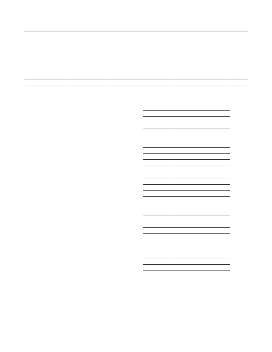
PARAMETER
SYMBOL
CONDITIONS
MIN
TYP
MAX
UNITS
Maximum Fast-Charge
Time
t
FCHG
FChgTmr[1:0] = 00
75
Min
FChgTmr[1:0] = 01
150
FChgTmr[1:0] = 10
300
FChgTmr[1:0] = 11
600
Maintain Charge Time
t
TOCHG
MtChgTmr[1:0] = 00
0
Min
MtChgTmr[1:0] = 01
15
MtChgTmr[1:0] = 10
30
MtChgTmr[1:0] = 11
60
Timer Accuracy
t
ACC
-10
+10
%
Timer Extend Threshold
P
TIMERX
If charge current is reduced due to
I
LIM
or T
DIE
, this is the percentage
of charge current below which
timer clock operates at half speed
50
%
Timer Suspend
Threshold
P
TIMERSUS
If charge current is reduced due to
I
LIM
or T
DIE
, this is the percentage
of charge current below which
timer clock pauses
20
%
THERMISTOR MONITOR AND NTC DETECTION
THM Hot Threshold
T4
V
THM
falling, WarmCoolSel = 0
21.3
23.3
25.3
%V
TPU
V
THM
falling, WarmCoolSel = 1
30.9
32.9
34.9
THM Warm Threshold
T3
V
THM
falling, WarmCoolSel = 0
30.9
32.9
34.9
%V
TPU
V
THM
falling, WarmCoolSel = 1
46.5
50
53.5
THM Cool Threshold
T2
V
THM
rising, WarmCoolSel = 0 or 1
62.5
64.5
66.5
%V
TPU
THM Cold Threshold
T1
V
THM
rising, WarmCoolSel = 0 or 1
71.9
73.9
75.9
%V
TPU
THM Disable Threshold
V
THM_DIS
V
THM
rising
91.0
93.0
95.0
%V
TPU
THM Threshold Hysteresis
V
THM_DIS_H
60
mV
JEITA BAT Voltage
Reduction
V
BAT_JEITA
300
mV
THM Input Leakage
I
THM_LK
-1
+1
µA
THM Detection Time
t
THM_DET
0.35
ms
DIGITAL I/O (SDA, SCL,
FLTIN
, INT, SYSOK, FSUS, LED, CDIR)
Leakage Current
I
IO_LK
-1
+1
µA
Logic Input High-Voltage
V
IO_IH
1.4
V
Logic Input Low-Voltage
V
IO_IL
0.5
V
Logic Output Low-Voltage
V
IO_OL
I
OL
= 4mA
0.4
V
FSUS Input Pulldown
Resistance
R
FSUS_PD
470
kΩ
SDA, SCL Bus Low-
Detection Current
I
PD
V
SDA
= V
SCL
= 0.4V
0.2
0.4
µA
SCL Clock Frequency
f
SCL
Note 3
0
400
kHz
MAX14748
USB Type-C Charger
www.maximintegrated.com
Maxim Integrated
8
Electrical Characteristics (continued)

(V
BAT
= 8.3V, T
A
= -40 °C to +85 °C, all registers in their default state, unless otherwise noted. Typical values are at V
CHGIN
= 5.0V,
V
BAT
=7.4V, V
SYS
= V
BATREG
, T
A
= +25 °C.)
PARAMETER
SYMBOL
CONDITIONS
MIN
TYP
MAX
UNITS
Bus Free Time Between
a STOP and START
Condition
t
BUF
1.3
µs
START Condition
(Repeated) Hold Time
t
HD_SDA
Note 3
0.6
µs
Low Period of SCL
Clock
t
LOW
1.3
µs
High Period of SCL
Clock
t
HIGH
0.6
µs
Setup Time for a
Repeated START
Condition
t
SU_STA
0.6
µs
Data Hold Time
t
HD_DAT
Note 4
0
0.9
µs
Data Setup Time
t
SU_DAT
Note 4
100
ns
Setup Time for STOP
Condition
t
SU_STO
0.6
µs
Spike Pulse Widths
Suppressed by Input
Filter
t
SP
Note 5
50
ns
BC1.2 DETECTION
V
DP_SRC
Voltage
V
DP_SRC
/V
SRC06
I
LOAD
= 0 to 200 µA
0.5
0.6
0.7
V
V
DM_SRC
Voltage
V
DM_SRC
/V
SRC06
I
LOAD
= 0 to 200 µA
0.5
0.6
0.7
V
V
D33
Voltage
V
SRC33
I
LOAD
= 0 to 365 µA
2.6
3.4
V
V
DAT_REF
Voltage
V
DAT_REF
0.25
0.32
0.4
V
V
LGC
Voltage
V
LGC
1.5
1.7
1.9
V
I
DM_SINK
Current
I
DM_SINK
/I
DATSINK
0.15V to 3.6V
55
80
105
µA
I
DP_SRC
Current
I
DP_SRC
/I
DCD
0V to 2.5V
7
10
13
μA
R
DM_DWN
Resistor
R
DM_DWN
/R
DWN15
12
20
24
kΩ
I
WEAK
Current
I
WEAK
0.01
0.1
0.5
µA
V
BUS31
Threshold
V
BUS31
DP and DN pins. Threshold in
percent of V
BUS
voltage
4V < V
BUS
< 5.5V
26
31
36
%
V
BUS47
Threshold
V
BUS47
DP and DN pins. Threshold in
percent of V
BUS
voltage
4V < V
BUS
< 5.5V
43.3
47
51.7
%
V
BUS64
Threshold
V
BUS64
DP and DN pins. Threshold in
percent of V
BUS
voltage
4V < V
BUS
< 5.5V
57
64
71
%
MAX14748
USB Type-C Charger
www.maximintegrated.com
Maxim Integrated
9
Electrical Characteristics (continued)

(V
BAT
= 8.3V, T
A
= -40 °C to +85 °C, all registers in their default state, unless otherwise noted. Typical values are at V
CHGIN
= 5.0V,
V
BAT
=7.4V, V
SYS
= V
BATREG
, T
A
= +25 °C.)
PARAMETER
SYMBOL
CONDITIONS
MIN
TYP
MAX
UNITS
Charger Detection Debounce
t
CDDEB
45
50
55
ms
Primary-to-Secondary Timer
t
PDSDWAIT
27
35
39
ms
Proprietary Charger
Debounce
t
PRDEB
5
7.5
10
ms
Data Contact Detect
Timeout
t
DCDTMO
DCD2s = 0
700
800
900
ms
DCD2s = 1
1.8
2.0
2.2
DP/DN Overvoltage
Debounce
t
OVDXDEB
90
100
110
µs
OVDX Comparator
OVDX
THRESHOLD
Rising
0
0.15
V
Falling
-0.04
+0.08
CDP/CDN Pulldown
Resistor
R
CDP/CDN_PD
3
6
12
mΩ
TYPE-C DETECTION
V
CONN
Switch Voltage Drop
V
CONN_REQ
V
CONN
= 5.5V, I
CC_LOAD
= 20mA
5.5
5.6
V
V
CONN
Bulk Capacitance
C
VCONN
10
220
µF
CC Pin Operational
Voltage Range
V
CONN_RNG
5.5
V
CC Pin Voltage in DFP
3.0A Mode
V
CC_PIN30
3.1
V
CC Pin Voltage in DFP
1.5A Mode
V
CC_PIN15
1.85
V
CC Pin Low-Power Mode
Pulldown Resistance
R
LPPD_CC_
170
kΩ
CC Pin Low-Power Mode
Voltage Threshold
V
LP_CC_
Rising
0.7
V
CC Pin Clamp Requirements
V
CC_PIN_CLAMP
60 µA ≤ I
CC_
≤ 600 µA
1.1
1.32
V
CC UFP Pulldown Resistance
R
DUFP_CC_
4.59
5.1
5.61
kΩ
CC DFP 0.5A Current
Source
I
DFP0.5_CC_
72
80
88
µA
CC DFP 1.5A Current
Source
I
DFP1.5_CC_
165.6
180
194.4
µA
CC DFP 3.0A Current
Source
I
DFP3.0_CC_
303.6
330
356.4
µA
CC R
A
and R
D
Threshold
V
RA_RD0.5
Rising
0.16
0.2
0.25
V
Falling
0.15
CC UFP 0.5A R
D
Threshold
V
UFP_RD0.5
Rising
0.62
0.66
0.7
V
Falling
0.61
CC UFP 1.5A R
D
Threshold
V
UFP_RD1.5
Rising
1.17
1.23
1.31
V
Falling
1.16
CC V
CONN
Detect
Threshold
V
VCONN_DET
Rising
2.11
2.25
2.4
V
Falling
2.1
MAX14748
USB Type-C Charger
www.maximintegrated.com
Maxim Integrated
10
Electrical Characteristics (continued)

(V
BAT
= 8.3V, T
A
= -40 °C to +85 °C, all registers in their default state, unless otherwise noted. Typical values are at V
CHGIN
= 5.0V,
V
BAT
=7.4V, V
SYS
= V
BATREG
, T
A
= +25 °C.)
PARAMETER
SYMBOL
CONDITIONS
MIN
TYP
MAX
UNITS
CC DFP V
OPEN
Detect
Threshold
V
DFP_VOPEN
Rising
1.51
1.575
1.65
V
Falling
1.5
CC DFP V
OPEN
with
3.0A Detect Threshold
V
DFP_VOPEN3A
Rising
2.46
2.6
2.75
V
Falling
2.45
V
V
BUS
Valid
V
BDET
Rising
3.8
4.12
4.4
V
V
BUS
Valid Hysteresis
V
BDET_H
Falling hysteresis
0.7
V
V
BUS
Discharge Value
V
SAFE0V
Falling. Voltage level where a
connected UFP will find V
BUS
removed.
0.6
0.7
0.84
V
Rising hysteresis
100
mV
CC Pin Power-Up Time
t
CLAMPSWAP
The maximum time allowed from
removal of voltage clamp to
attachment of the 5.1k resistor
15
ms
Type-C CC Pin
Detection Debounce
t
CCDEB
100
200
ms
Type-C Debounce
t
PDDEB
10
20
ms
Type-C Quick Debounce
t
QDEB
0.9
1
1.9
ms
V
BUS
Debounce
t
VBDEB
9
10
11
ms
V
SAFE0V
Debounce
t
VSAFE0VDEB
9
10
11
ms
Type-C Error Recovery
Delay
t
ERRORRECOVERY
25
ms
Type-C DRP Toggle
Time
t
DRP
50
100
ms
Duty Cycle of DRP
Swap
D
DRP
Duty cycle of UFP to DFP role
swap
30
70
%
DRP Transition Time
t
DRPTRAN
Time a role swap from DFP to UFP
or reverse is completed
1
ms
DRP Lock Time
t
DRPLOCK
DRP Lock wait time before
transition to unattached state
100
150
ms
V
CONN
Enable Time
t
VCONNON
Time from when V
BUS
is supplied
in DFP mode in state Attach.DFP.
DRPWait
10
ms
V
CONN
Disable Time
t
VCONNOFF
Time from UFP detached or as
directed by I
2
C command until
V
CONN
is removed
35
ms
MAX14748
USB Type-C Charger
www.maximintegrated.com
Maxim Integrated
11
Electrical Characteristics (continued)

(V
BAT
= 8.3V, T
A
= -40 °C to +85 °C, all registers in their default state, unless otherwise noted. Typical values are at V
CHGIN
= 5.0V,
V
BAT
=7.4V, V
SYS
= V
BATREG
, T
A
= +25 °C.)
Note 2: All devices are 100% production tested at T
A
= +25 °C. Limits over the operating temperature range are guaranteed by
design and characterization.
Note 3: f
SCL
must meet the minimum clock low time plus the rise/fall times.
Note 4: The maximum t
HD:DAT
has to be met only if the device does not stretch the low period (t
LOW
) of the SCL signal.
Note 5: Filters on SDA and SCL suppress noise spikes at the input buffers and delay the sampling instant.
PARAMETER
SYMBOL
CONDITIONS
MIN
TYP
MAX
UNITS
CC Pin Current Change
Time
t
SINKADJ
Time from CC pin changes state in
UFP mode until current drawn from
DFP reaches new value
60
ms
V
BUS
On-Time
t
VBUSON
Time from UFP is attached until
V
BUS
On
275
ms
V
BUS
Off-Time
t
VBUSOFF
Time from UFP is detached until
V
BUS
reaches V
SAFE0V
650
ms
BVCEN Output Low-
Voltage
V
BVCEN_OL
I
SINK
= 1mA
0.4
V
BVCEN Output High-
Voltage
V
BVCEN_OH
I
SOURCE
= 1mA
V
CCINT
- 0.4
V
MAX14748
USB Type-C Charger
www.maximintegrated.com
Maxim Integrated
12
Electrical Characteristics (continued)

(V
BAT
= 8.5V, T
A
= -20 °C to +70 °C, all registers in their default state, unless otherwise noted. Typical values are at V
CHGIN
= 5.0V,
V
BAT
=7.4V, V
SYS
= V
BATREG
, T
A
= +25 °C.)
MAX14748
USB Type-C Charger
Maxim Integrated
13
www.maximintegrated.com
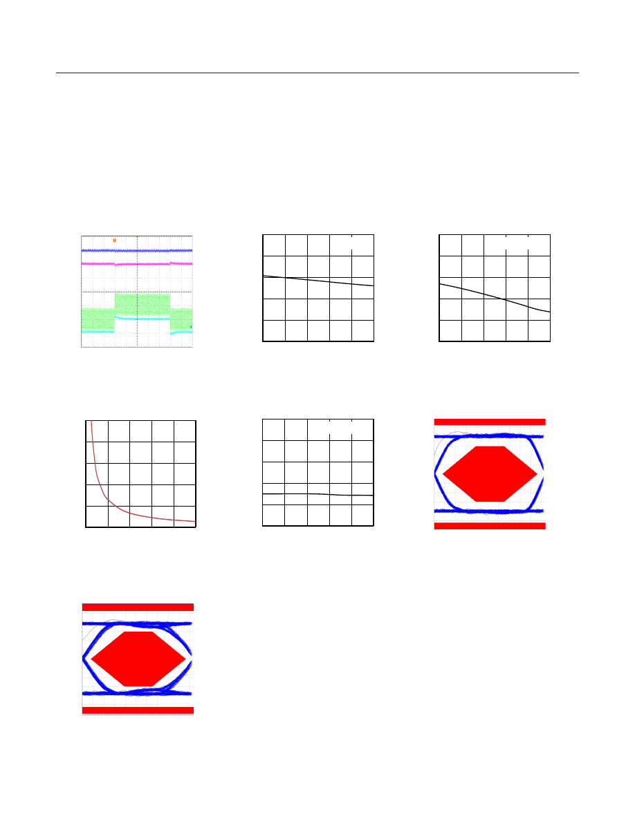
Typical Operating Characteristics
7
7.2
7.4
7.6
7.8
8
0
800
1600
2400
3200
V
SYS
(V
)
I
CHGIN
(mA)
V
SYS
vs. I
CHGIN
toc04
V
BAT
= 7.4V
SpvChgILim[4:0] = 11101
SpvChgILim[4:0] = 01110
SpvChgILim[4:0] = 00100
4.9
4.94
4.98
5.02
5.06
5.1
0
100
200
300
400
500
V
CHG
IN
(V
)
I
CHGIN
(mA)
BUCK OUTPUT LOAD REGULATION
toc05
V
BAT
= 7.4V
50
60
70
80
90
100
0
300
600
900
1200
1500
EF
FI
CI
ENCY
(%
)
I
SYS
(mA)
BOOST EFFICIENCY vs. LOAD
toc06
V
BAT
= 6.0V
V
BAT
= 8.6V
V
BAT
= 7.4V
INPUT: CHGIN
OUTPUT: SYS
L1 = BOURNS SRP4012TA-2R2M
0
40
80
120
160
200
6
7
8
9
BA
TT
ER
Y I
NP
UT
CURRE
NT
I
BA
T
( µ
A)
BATTERY VOLTAGE V
BAT
(V)
I
BAT
vs. V
BAT
toc01
LOW POWER MODE,
CHGIN FLOATING
TYPE-C ADAPTER
ATTACHED
NOT LOW POWER
MODE, CHGIN FLOATING
ChgEn =0
0
0.4
0.8
1.2
1.6
2
0
2
4
6
8
10
0.00
50.00
100.00
150.00
200.00
250.00
BA
TT
ER
Y CURRE
NT
(A
)
BA
TT
ER
Y VO
LT
AG
E (
V)
TIME (MINUTE)
I
BAT
and V
BAT
vs. TIME
toc02
2200mAH BATTERY
ChgDone[1:0] = 00
IPChg[1:0] = 00
VPChg[2:0] = 001
R
SET
= 10k
W
VOLTAGE
CURRENT
6.5
6.9
7.3
7.7
8.1
8.5
0
500
1000
1500
2000
V
SYS
(V
)
I
SYS
(mA)
V
SYS
vs. I
SYS
toc03
V
BAT
= 7.4V
SpvChgILim[4:0] = 11101
SpvChgILim[4:0] = 01110
SpvChgILim[4:0] = 00100
50
60
70
80
90
100
0
100
200
300
400
500
EF
FI
CI
ENCY
(%
)
I
CHGIN
(mA)
REVERSE BUCK
EFFICIENCY vs. LOAD
toc07
BBFrxZX = 0
INPUT: BAT
OUTPUT: CHGIN
L1 = BOURNS SRP4012TA-2R2M
BBFrxZX = 1
toc08
2ms/div
BOOST TRANSIENT RESPONSE
V
SYS
1V/div
I
SYS
500mA/div
V
BAT
= 7.4V,
ChgEn = 0
500mA/div
toc09
200
ms/div
BUCK TRANSIENT RESPONSE
(BBFrxZX = 1)
V
SYS
1V/div
I
CHGIN
V
CHGIN
I
INDUCTOR
500mA/div
1V/div
(V
BAT
= 8.5V, T
A
= -20 °C to +70 °C, all registers in their default state, unless otherwise noted. Typical values are at V
CHGIN
= 5.0V,
V
BAT
=7.4V, V
SYS
= V
BATREG
, T
A
= +25 °C.)
MAX14748
USB Type-C Charger
Maxim Integrated
14
www.maximintegrated.com
Typical Operating Characteristics (continued)
0
400
800
1200
1600
2000
0
20
40
60
80
100
B
A
T
T
E
R
Y
CURRE
NT
(
m
A
)
R
SET
(k
W)
FAST CHARGE CONSTANT
CURRENT vs. R
SET
toc13
500mA/div
toc10
200
ms/div
BUCK TRANSIENT RESPONSE
(BBFrxZX = 0)
V
SYS
1V/div
I
CHGIN
V
CHGIN
I
INDUCTOR
500mA/div
1V/div
toc16
TIME (0.2ns/div)
EYE DIAGRAM
(WITH DEVICE PRESENT)
U
SB D
IF
FER
EN
TI
AL
SI
G
N
AL
(V)
0.1V/div
V
L3OUT
= 3.0V
I
SYS
= 300mA
40
44
48
52
56
60
-40
-15
10
35
60
85
CHA
RG
ING
CURRE
NT
I
BA
T
(mA
)
TEMPERATURE ( °C)
PRECHARGE CURRENT vs.
TEMPERATURE
toc11
R
SET
= 10k
W
IPChg[1:0] = 00
900
940
980
1020
1060
1100
-40
-15
10
35
60
85
CHA
RG
ING
CURRE
NT
I
BA
T
(mA
)
TEMPERATURE ( °C)
FAST CHARGE CONSTANT
CURRENT vs. TEMPERATURE
toc12
R
SET
= 10k
W
8
8.2
8.4
8.6
8.8
9
-40
-15
10
35
60
85
BA
TT
ER
Y R
EG
U
LA
TI
O
N
VO
LT
AG
E (
V)
TEMPERATURE ( °C)
BATTERY REGULATION
VOLTAGE vs. TEMPERATURE
toc14
R
SET
= 10k
W
toc15
TIME (2ns/div)
EYE DIAGRAM
(WITHOUT DEVICE PRESENT)
U
SB D
IF
FER
EN
TI
AL
SI
G
N
AL
(V)
0.1V/div
MAX14748
USB Type-C Charger
www.maximintegrated.com
Maxim Integrated
15
Bump Configurations
1
2
3
4
A
B
C
D
GND
THM
VTPU
GND
BREG
FSUS
E
5
SYSOK
NVP
SDA
LED
GND
CC1
SCL
CC2
CDN
6
FLINT
COMP
CHGIN
GND
F
CDIR
CDP
TDP
CHGIN
INT
VCONN
BST
TPU
DGND
TDN
SYS
SET
BYP
PGND
LX
SYS
BAT
BYP
PGND
LX
7
CHGIN
CHGIN
SYS
BAT
BYP
PGND
LX
SYS
BAT
BYP
PGND
LX
8
9
TOP VIEW
(BUMP SIDE DOWN)
MAX14748
WLP
3.968mm x 2.768mm
VCCINT
SFOUT
BVCEN

BUMP
NAME
FUNCTION
A1
AGND
Analog Ground.
A2
FLTIN
Charger Fault Input. Logic-low on this pin forces the charger into a fault state and generates an
interrupt. See Register 0x35 description for more information. Connect to digital I/O supply if not used.
A3
SYSOK
Open-Drain Status Output of SYS Regulation. When V
SYS
is above the SYS UVLO threshold and Boost
is active, this output is high-impedance. When V
SYS
is below the SYS UVLO threshold, this output is
low. Leave unconnected if not used.
A4
TPU
High-Side of Internal Resistor for THM Detection. Connect a 10k resistor between this pin and THM.
A5
COMP
Buck/Boost Converter Compensation Connection. Connect a 3.9nF capacitor for internal Buck/Boost
compensation
A6
SET
External Resistor Connection for Fast Charge Current Setting. Connect a resistor to this pin to set the
fast charge current. Other charge currents are set as a proportion of fast charge current based on I
2
C
register settings.
A7-A9
BAT
Battery Connection. Connect a 2s Li-ion+ battery from BAT to GND. Bypass to PGND with a parallel combination
of a 0.1 µF capacitor and an effective 10 µF - 30 µF capacitor. Keep the capacitors as close to BAT as possible and
keep the stray inductance and resistance of the trace from BAT to the battery terminal as low as possible.
B1
CC2
USB Type-C CC2. Connect to CC2 on USB Type-C connector.
B2
FSUS
Force Suspend Input. Logic-high on this pin causes the input limiter to open and input current from CHGIN is reduced
to zero. This pin is internally pulled to GND through a 470kΩ (typ) resistor and has no effect if FSUSMsk = 1.
B3
DGND
Digital Ground.
B4
V
TPU
External Voltage Input for TPU connection. Connect to external supply or V
CCINT
.
B5
BREG
Bypass for Internal Switching Converter Supply. Bypass with 1 µF capacitor to AGND.
B6-B9
SYS
System Load Connection. Connect SYS to the system load. Bypass to PGND with a parallel combination
of a 0.1 µF capacitor and an effective 22 µF capacitor. (Note: there is a diode between SYS and BAT)
C1
V
CONN
External V
CONN
Supply Input. Leave unconnected if not used.
C2
SCL
I
2
C Serial Clock Input. Connect an external pull-up resistor.
C3
V
CCINT
Bypass For Internal Analog Supply. Bypass with 1 µF capacitor to GND.
C4, D4,
D5
GND
Ground.
C5
BST
Charge Pump Connection. Connect a 0.1 µF capacitor between BST and LX.
C6, C7,
C8, C9
LX
Switching Node of Boost Converter. Connect a 1.5 µH or 2.2 µH inductor between LX and BYP. See
Applications Information section for more details.
D1
CC1
USB Type-C CC1. Connect to CC1 on USB Type-C connector.
D2
SDA
I
2
C Serial Data Input/Output. Connect an external pullup resistor.
D3
INT
Active-Low, Open-Drain Interrupt Output. Connect an external pullup resistor.
D6, D7,
D8, D9
PGND
Power Ground.
MAX14748
USB Type-C Charger
www.maximintegrated.com
Maxim Integrated
16
Bump Description

BUMP
NAME
FUNCTION
E1
CDN
USB Connector D-Input. Leave unconnected if not used.
E2
LED
LED Charging Status Indicator. Open-drain output indicating battery charging status. When LEDAuto = 1 and
a temperature fault is detected, the output is pulsed at 50% duty cycle for a period of 1.5s. When a charge
timer expires or SysFlt fault occurs, LED is pulsed at 50% for a period of 0.15s. When LEDAuto = 0, the open-
drain output is controlled by the LEDCtrl bit. Connect this pin to GND if unused.
E3
THM
Battery Temperature Thermistor Measurement Connection. This pin is used for NTC thermistor presence
detection and JEITA compliant temperature control.
E4
SFOUT
Output of overvoltage protected LDO powered from CHGIN. Bypass SFOUT with a 1 µF ceramic
capacitor to GND.
E5
CDIR
USB Cable Orientation Open-drain Output. When CC1 is active, this output is pulled low. Otherwise, this
output is high-impedance. Leave unconnected if not used.
E6-E9
BYP
Bypass Connection. Bypass to PGND with a parallel combination of a 0.1 µF capacitor and an effective
10 µF capacitor.
F1
CDP
USB Connector D+ Input. Leave unconnected if not used.
F2
TDP
USB Transceiver D+ Connection. Connect TDP to device microprocessor USB transceiver D+ line.
Leave unconnected if not used.
F3
TDN
USB Transceiver D- Connection. Connect TDN to device microprocessor USB transceiver D- line. Leave
unconnected if not used.
F4
BVCEN
External V
CONN
Supply Enable Output. Push-pull output between V
CCINT
and GND. Leave
unconnected if not used.
F5
NVP
Negative Voltage PFET Gate Control. Leave unconnected if not used.
F6-F9
CHGIN
USB Charger Input. Bypass this pin with a 1 µF capacitor to PGND.
Note: All capacitance values listed in this document refer to effective capacitance. Be sure to specify capacitors that will meet these
requirements under typical system operating conditions taking into consideration the effects of voltage and temperature.
MAX14748
USB Type-C Charger
www.maximintegrated.com
Maxim Integrated
17
Bump Description (continued)
MAX14748
USB Type-C Charger
www.maximintegrated.com
Maxim Integrated
18
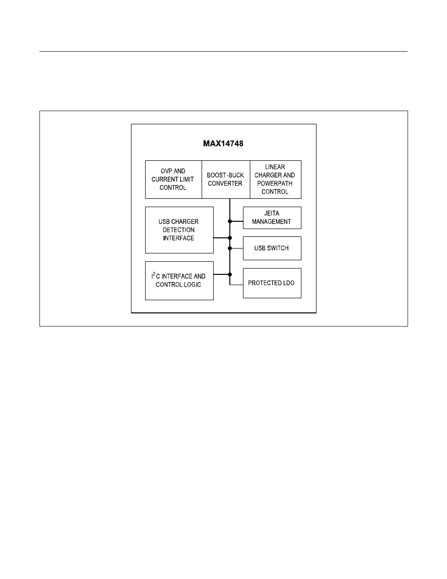
Block Diagram

Detailed Description
The MAX14748 is a battery charger with a Smart Power
Selector that safely charges two Li+ cell in accordance
with JEITA specifications*.
Input OVP
The MAX14748 CHGIN input is protected by an internal
N-channel FET. The device monitors the voltage at
CHGIN and, if CHGIN is greater than V
OVP
, switches
off the internal FET to prevent damage to the device.
If V
CHGIN
is above the overvoltage threshold or below
the USB valid voltage threshold, the MAX14748 enters
overvoltage lockout (OVLO). During OVLO, the internal
circuits remain powered, the SYSOK pin is high-impedance,
and an interrupt is asserted. During OVLO, the charger
turns off and the system load switch closes, allowing the
battery to power SYS.
Negative Voltage Protection (NVP)
The MAX14748 provides a gate protection circuit for an
external PFET that protects against negative voltages on
V
BUS
. NVP pin drives the gate of the external PFET. If a
negative voltage is present on V
BUS
, e.g., by a backwards
connector, the NVP turns off the external PFET, therefore
providing negative voltage protection.
Low Power Mode
The MAX14748 features a Low Power mode, which
reduces the battery current consumption from 25 µA to
140 µA. To enter Low Power mode, write 1 to LowPowEn
(Register 0x33[7]). To manually exit Low Power mode,
set LowPowAbort (Register 0x33[1]) to 1. If a DFP pullup
connect to CC1/CC2 is detected, the device automatically
exits Low Power mode and resumes normal operations.
Input Current Limiter
The primary function of the input limiter is supplying
power from the external adapter at CHGIN to the system
load and battery charger. In addition, it performs several
other functions to optimize use of the available power
efficiently and safely, including:
1) CHGIN Input Current Limiting: The CHGIN input current is
limited to prevent input overload. The current limit can be
automatically selected through charger detection to match
the capabilities of the source. The result is indicated by
for more
details. It can also be manually set through CurLim1Frc
illustrates
how the current limit setting is selected.
2) Thermal Limiting: In case the die temperature
exceeds the normal limit (T
CHG_LIM
), the MAX14748
will attempt to limit temperature increase by reducing
the input current at CHGIN. In this condition, the
system load has priority over charger current, so the
input current is first reduced by lowering the charge
current. If the junction temperature continues to rise
and reaches the maximum operating limit (T
BUS_LIM
),
no input current is drawn from CHGIN and the battery
powers the entire system load.
3) Adaptive Battery Charging: While the system is
powered from CHGIN, the charger draws power from
SYS to charge the battery. If the total load exceeds
the input current limit, the battery supplies supplmental
current to the load.
4) Adaptive Input Current Limiting: If the MAX14748
input current limit is programmed in such a way that
the adapter voltage collapses due to resistive drop,
current limiting, or poor load transient response,
the AICL loop allows the MAX14748 to regulate the
input voltage above a value needed to ensure proper
operation.
the AICL block and associated parameters are found
in the registers 0x2C to 0x2E.
*JEITA (Japan Electronics and Information Technology Industries Association) Standard, A Guide to the Safe Use of Secondary
Lithium Ion Batteries on Notebook-Type Personal Computers, April 20, 2007.
MAX14748
USB Type-C Charger
www.maximintegrated.com
Maxim Integrated
19

Table 1a. Automatic Input Current Limit Control
ChgTyp[1:0]
PrChgTyp[2:0]
CCIStat[1:0]
SDPMaxCur[1:0] CDPMaxCur[1:0]
I
LIM
SpvChgIlim[4:0]
xx
xxx
11 = 3A
00
0
3A
0x1D
11 = 1.5A
xxx
11 = 3A
xx
x
3A
0x1D
xx
110 = 3A
xx
xx
x
3A
0x1D
xx
101 = 2.4A
00 or
01 = 500mA or
10 = 1.5A
xx
x
2.4A
0x17
xx
100 = 2A or
001 = 2A
00 or
01 = 500mA or
10 = 1.5A
xx
x
2A
0x13
1x = 1.5A
000 or
010 = 500mA
00 or
01 = 500mA or
10 = 1.5A
xx
x
1.5A
0x0E
1x = 1.5A
000 or
010 = 500mA
or 011 = 1A
10 = 1.5A
xx
x
1.5A
0x0E
xx
011 = 1A
00 or
01 = 500mA
xx
x
1A
0x09
01 = 500mA
000 or 010 =
500mA
00 or
01 = 500mA
xx
x
0.5A
0x04
01 = 500mA
000
10 = 1.5A or
11 = 3A
01
x
0.5A
0x04
01 = 500mA
000
10 = 1.5A or
11 = 3A
10
X
1.0A
0x09
01 = 500mA
000
10 = 1.5A or
11 = 3A
11
x
1.5A
0x0E
10 = 1.5A
000
11 = 3A
xx
1
1.5A
0x0E
00
xxx
xx
xx
x
NA
NA
MAX14748
USB Type-C Charger
www.maximintegrated.com
Maxim Integrated
20
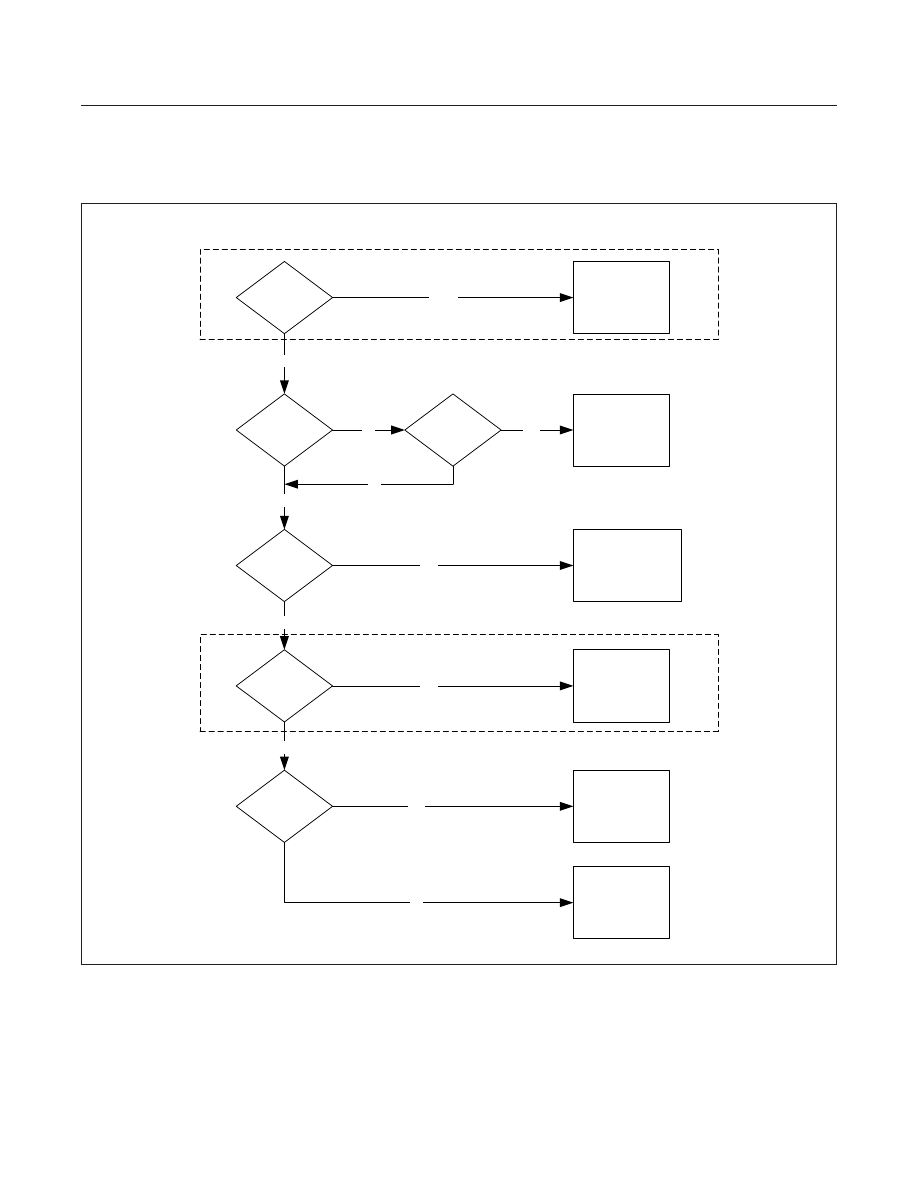
Figure 1. Input Current Limit Settings Flow Diagram
MAX14748
USB Type-C Charger
www.maximintegrated.com
Maxim Integrated
21
NO
NO
NO
YES
YES
T
DIE
> 150 °C
ILIM = 0
ILIM = 0
ILIM = WEAK BATTERY
CURRENT LIMIT
FSUS PIN =
HIGH
FSUSMsk = 1
WEAK
BATTERY
YES
YES
YES
NO
CurLim1Frc
ILIM = CurLim1Set[4:0]
value
AICLAbort = 0
AND AICLEn =1
ILIM SET BY AICL
ILIM = Auto
(USB-C/BC1.2)
NO
NO
FAULT CONDITION
MANUAL SETTING
YES
Figure 2. AICL Operation Flow Diagram
MAX14748
USB Type-C Charger
www.maximintegrated.com
Maxim Integrated
22
AICL INCREMENT
INPUT CURRENT = MIN
(STOP CURRENT, INPUT CURRENT + 100mA)
AICL PRECHECK
STOP CURRENT = AICLMaxI[4:0]
INPUT CURRENT = PREVIOUS SETTING
AICL IDLE
INPUT CURRENT = STOP CURRENT
AICL BLANK
INPUT CURRENT = 0,
STOP CURRENT = INPUT CURRENT - 100mA
VBDET MASKED AND OVP CLOSED
AICLAbort = 0 AND
AICLEn = 1
V
BYP
< V
BYPUVLO
AND TBLANK TIMEOUT
V
BYP
> V
BYPUVLO
AND
V
CHGIN
> V
BDET
V
BYP
< V
BYPUVLO
AICL OFF
STOP CURRENT = 500mA
MIN CURRENT = 100mA
INPUT CURRENT = PREVIOUS SETTING
AICL INIT
INPUT CURRENT = MIN CURRENT
V
BYP
> V
BYPUVLO
AND
INPUT CURRENT = STOP CURRENT
V
BYP
< V
BYPUVLO
TSTEP
TIMEOUT
AICLAbort = 1
AICLEn = 1
AICL NO CONNECTION
INPUT CURRENT = PREVIOUS SETTING
STOP CURRENT = 500mA
ChgStat[3:0] 0011

Boost Converter with Reverse Buck
Boost Mode
The MAX14748 boost converter operates as either a
current-limited voltage source, or current source, depending
on the charger operational state. When a valid USB voltage
is present at CHGIN, and the charger is disabled, V
SYS
is regulated to V
BAT
+ 400mV. If the charger is in
precharge mode, V
SYS
is regulated to V
PCHG
+ 400mV.
When the system is in fast-charge mode, the boost
converter operates as a current source, delivering
current into the SYS node that is shared by the battery
and system loads.
The boost converter current limit may be acted upon
by multiple system blocks, including the programmed
input current limit, thermal status, charging current, SYS
regulation voltage block, and battery termination voltage
block. The minimum requested current from these blocks
at any given time determines the active current limit in
the boost.
Reverse Buck Mode
The CHGIN-SYS switching converter may operate as a
buck converter when needed to supply a load attached to
CHGIN. The load may be a Type-C sink or some other
proprietary device.
If Type-C DRP operation is enabled, the buck converter
can be enabled by the Type-C state machine. The output
voltage of the buck can be programmed from 4V to 5.5V
in 0.1V steps by writing to BuckVSet[3:0], however, it is
not recommended to change the output voltage when the
buck is active.
The output of the buck converter turns off when a
fault occurs. The specific fault occurred is indicated by
DCDCILim, DCDCRunAway, DCDCPGood status bits
(register 0x04). See Register Descriptions for more
details. When the buck is disabled due to a fault, both
VBUSDet (register 0x07) and VSAFE0V (register 0x0A)
change to 0. After the fault condition is removed, the buck
converter can be restarted by writing 1 to CCSnkRst,
CCSrcRst, CCForceError, or USBCRset auto-reset bits.
MAX14748
USB Type-C Charger
www.maximintegrated.com
Maxim Integrated
23

Smart Power Selector
The Smart Power Selector seamlessly distributes power
between CHGIN, battery (BAT) and the system (SYS).
The basic modes of operation of the smart power selec-
tor are:
1. With a valid external power source:
a. The external power source at CHGIN is the
primary source of energy.
b. The battery is the secondary source of energy.
c. Energy delivery to SYS is the highest priority.
d. Any energy that is not required by SYS is available
to the battery.
2. With no power source available at CHGIN:
a. The battery is the primary source of energy.
b. Energy delivery to SYS has the highest priority.
3. With a Type-C Sink or other load present at CHGIN:
a. The battery is the primary source of energy.
b. Energy delivery to SYS is the highest priority.
c. Energy delivery to BYP is the second highest
priority.
4. SYS Regulation Voltage:
a. When the charger path is enabled and the
charger is disabled, V
SYS
is regulated to V
BAT
+
400mV and BAT switch is off.
b. When the charger is enabled but in a non-charging
state such as maitain charge done, thermistor
suspend, or timer fault, V
SYS
is regulated to
V
BAT
+ 400mV and BAT switch is off.
c. When the input charger path is enabled and the
battery is charging in prequalification, V
SYS
is
regulated to V
PCHG
+ 400mV. Charge current is
reduced when V
SYS
approaches V
PCHG
+ 200mV.
d. When the input charger path is enabled and the
battery is charging in fast-charge or maintain charge
done, the BAT switch is closed and V
SYS
= V
BAT
. In
maintain charge done state, the connection between
SYS and BAT acts as an ideal diode. Therefore,
when V
SYS
drops below V
BAT
, the BAT switch is
turned fully on and the battery supplements the SYS
load along with the current from CHGIN.
e. When the switching converter is enabled as a
reverse buck, the BAT switch is closed and
V
SYS
= V
BAT
.
Short-Circuit Protection
The MAX14748 provides short-circuit protection to the
power nodes. When SYS is shorted to ground, input
current from CHGIN is limited by boost converter current
limit. Note in this case, FET diode from BAT-SYS prevents
control of FET BAT-SYS current. Battery current is not
limited by the MAX14748 and a pack protector is needed
to limit the battery current.
When either BYP or CHGIN is shorted to ground, the current
from BAT is limited by the reverse buck converter.
USB Type-C 1.1
USB Type-C 1.1 UFP and DRP Support
The MAX14748 provides support for devices functioning as
a Upstream Facing Port (UFP) or Dual Role Port (DRP)
per the current USB Type-C 1.1 specification. When acting
as a power source in DRP mode, the MAX14748 can provide
a 5V V
BUS
on the CHGIN pin through operation of the
reverse buck converter. The USB Type-C V
CONN
supply
is provided externally via the V
CONN
pin, and switched
internally onto one of the CC pins. An open-drain output
pin, BVCEN, is provided to enable the external V
CONN
supply based on the Type-C state machine output.
BVCEN is a push-pull output between GND and V
CCINT
.
USB BC1.2 Compliant and Nonstandard Charger
Support
The BC1.2 charger detection and special charger detection
routine is embedded within the Type-C state machine.
The BC1.2 and Special Charger detection routine runs
always when the state machine enters the AttachWait.
SNK state of the USB Type-C 1.1 state-machine.
USB Type-C Adapter Insertion
and
depict the general timings when
a USB Type-C adapter is attached. For more information
on the behavior and timings of the USB Type-C 1.1 state-
machine, please refer to the USB Type-C specification.
MAX14748
USB Type-C Charger
www.maximintegrated.com
Maxim Integrated
24
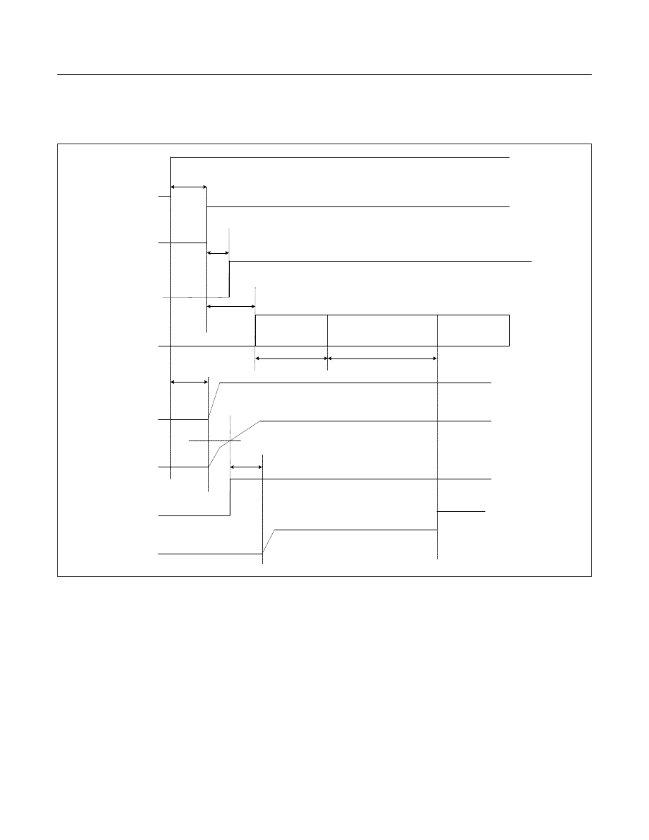
Figure 3a. Type-C Adapter Insertion (CHGINILimGate = 0)
MAX14748
USB Type-C Charger
www.maximintegrated.com
Maxim Integrated
25
BYP
V
SYS
SYSOK
I
BAT
35ms (TYP)
CHGIN
CC
0ms (MIN),
485ms (MAX)
DCD
CHARGER DETECTION
UPDATE CURRENT
CAPABILITY
10ms (TYP)
900ms(MAX)
250ms (MAX)
150ms (MIN),
485ms (MAX)
ChgDet
SFOUT
20ms (TYP)
V
SYSUVLO
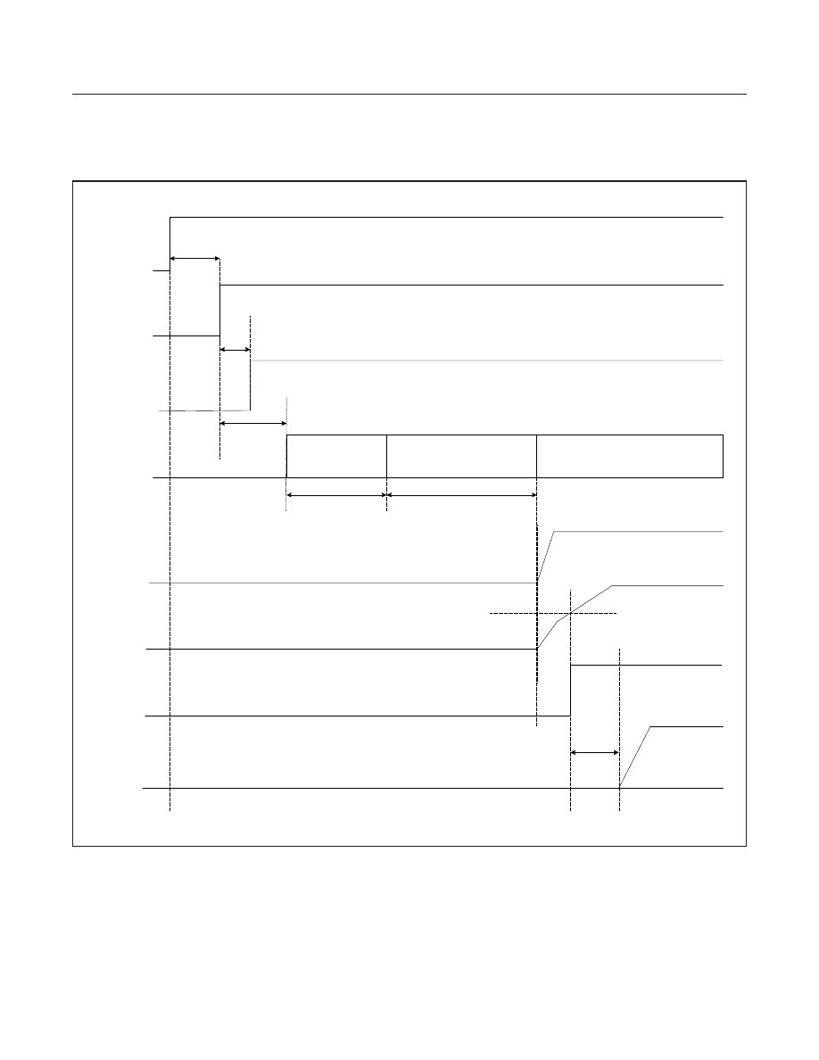
Figure 3b. Type-C Adapter Insertion (CHGINILimGate = 1)
MAX14748
USB Type-C Charger
www.maximintegrated.com
Maxim Integrated
26
BYP
V
SYS
SYSOK
I
BAT
CHGIN
CC
0ms (MIN),
475ms (MAX)
DCD
CHARGER DETECTION
UPDATE CURRENT CAPABILITY
10ms (TYP)
900ms(MAX)
250ms (MAX)
ChgDet
SFOUT
20ms (TYP)
V
SYSUVLO
35ms (TYP)
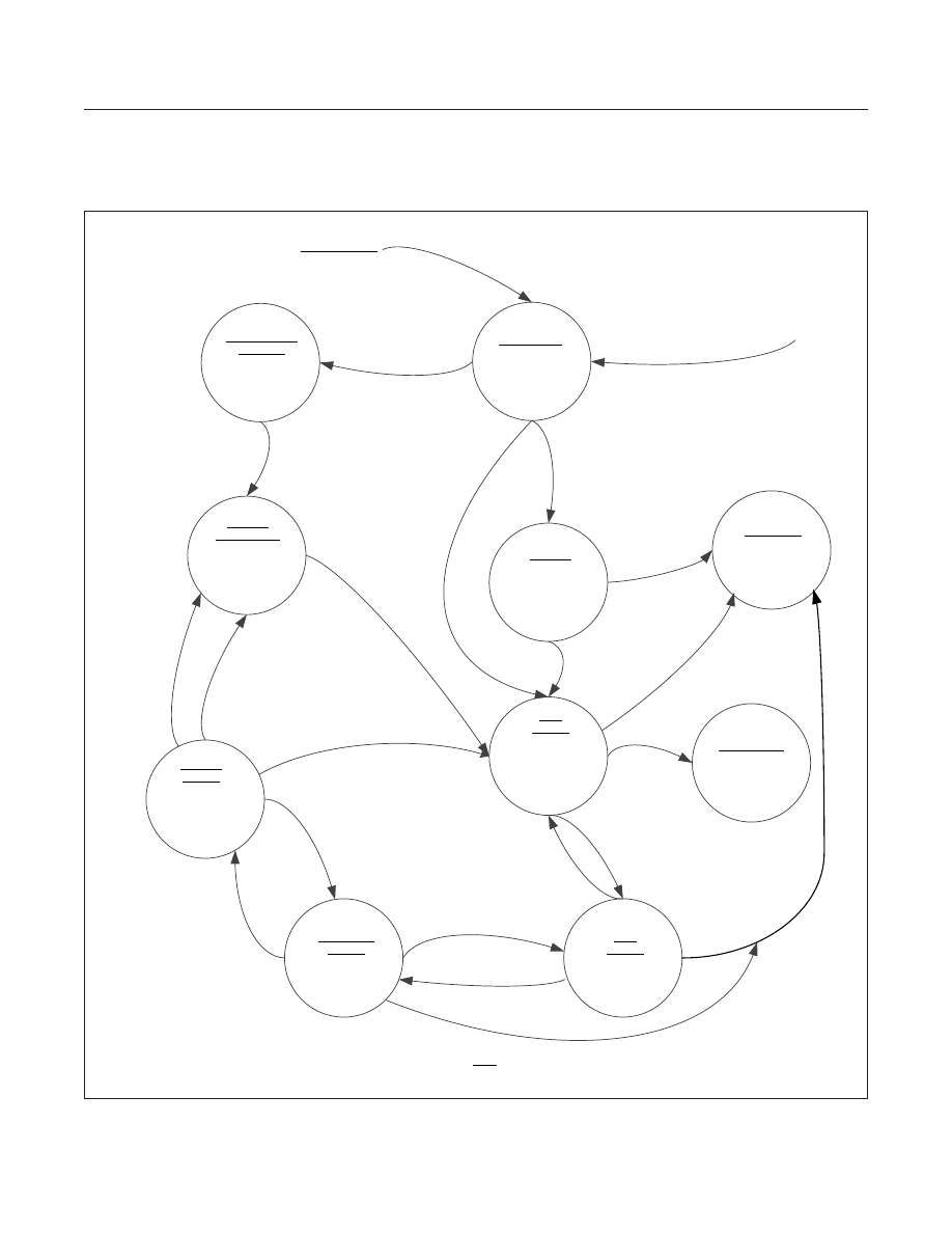
Figure 4. Battery Charger State Diagram
MAX14748
USB Type-C Charger
www.maximintegrated.com
Maxim Integrated
27
MAINTAIN
CHARGE DONE
ChgStat = 0110
LED = OFF
I
CHG
= 0
CHARGER OFF
ChgStat = 0000
LED = OFF
I
CHG
= 0
PREQUAL
ChgStat = 0010
LED = ON
I
CHG
= I
PCHG
FAST
CHARGE
(CONSTANT CURRENT)
ChgStat = 0011
LED = ON
I
CHG
= I
FCHG
**
FAST
CHARGE
(CONSTANT VOLTAGE)
ChgStat = 0100
LED = ON
MAINTAIN
CHARGE
ChgStat = 0101
LED = ON
I
CHG
< I
CHG_DONE
FRESH BATTERY
INSERTION
ChgStat = 0110
LED = 1s PULSE
I
CHG
= 0
TIMER FAULT
ChgStat = 0111
LED = 0.15s PERIOD
I
CHG
= 0
ChgEn = 1,
V
BAT
< V
BATREG
- V
BATRECHG
AND V
BAT
< V
PCHG_R
AND V
SYS
> V
BAT
+ TBDV
V
BAT
> V
PCHG_R
RESET CHARGE TIMER
V
BAT
< V
PCHG_R
VOLTAGE MODE
= 1*
VOLTAGE MODE
= 0*
RECOVER FROM FAULT RESET
CHARGE TIMER
ChgEn = 1,
V
BAT
>
V
BATREG
- V
BATRECHG
ChgEn = 1,
Fresh battery AND
V
BAT
>
V
BATREG
- V
BATRECHG
I
CHG
> I
CHG_DONE
and
VOLTAGE MODE = 1*
RESET CHARGE TIMER
I
CHG
< I
CHG_DONE
AND V
SYS
> V
SYS_LIM
AND T
DIE
< T
CHG_LIM
RESET CHARGE TIMER
I
CHG
> I
CHG_DONE
and
VOLTAGE MODE=0*
RESET CHARGE TIMER
t
CHG_TIMER
> t
MTCHG
AND
ChgAutoStp = 1
V
BAT
< V
BATREG
- V
BATRECHG
AND ChgAutoReSta = 1
AND V
SYS
> V
SYS_LIM
t
CHG_TIMER
> t
PCHG
t
CHG_TIMER
> t
FCHG
T
DIE
> T
BUS_LIM
OR V
BAT
> V
SYS
OR ChgEn=0
FROM ANY STATE
NOTES:
* VOLTAGE MODE IS AN INTERNAL SIGNAL
** CHARGE TIMER IS SLOWED BY 50% IF I
CHG
<I
FCHG
/2 AND PAUSED IF I
CHG
< I
FCHG
/5 ONLY IN FAST CHARGE CONSTANT CURRENT STATE
SYSTEM FAULT
ChgStat = 0111
LED = 0.15s PERIOD
I
CHG
= 0
JEITA VOLTAGE LIMITATION
AND ChgAutoStp = 1
V
BAT
< V
PCHG_R
ChgEn = 1,
V
BAT
< V
BATREG
- V
BATRECHG
AND V
BAT
> V
PCHG_R
AND V
SYS
> V
SYS_LIM
t
CHG_TIMER
> t
FCHG
LINEAR FAST
CHARGE
(CONSTANT VOLTAGE)
ChgStat = 0100
LED = ON
I
CHG
< 20% I
FCHG
V
BAT
< V
BATREG
- V
BATRECHG
Figure 5. Battery Charger State Diagram (continued)
MAX14748
USB Type-C Charger
www.maximintegrated.com
Maxim Integrated
28
PAUSE
CHARGE
TIMER
PAUSE
CHARGE
TIMER
PAUSE
CHARGE
TIMER
From PREQUAL
JEITA ERROR
To PREQUAL
NO JEITA ERROR
From FAST CHARGE CC
JEITA ERROR
From FAST CHARGE CV
JEITA ERROR
From FRESH BATTERY INSERTION ,
MAINTAIN CHARGE DONE ,
MAINTAIN CHARGE
JEITA ERROR
To CHARGER OFF
RESET CHARGE TIMER
NO JEITA ERROR
From PREQUAL
FLTIN = Low
To PREQUAL
FLTIN = High
From FAST CHARGE CC
FLTIN = Low
From FAST CHARGE CV
FLTIN = Low
To LINEAR FAST CHARGE
FLTIN = High
To CHARGER OFF
FLTIN = High
BATTERY FAULT
CHARGE SUSPEND
ChgStat = 1000
LED = 0.15s period
I
CHG
= 0
From FRESH BATTERY INSERTION ,
MAINTAIN CHARGE DONE ,
MAINTAIN CHARGE
FLTIN = Low
BATTERY TEMP
CHARGE SUSPEND
ChgStat = 0001
LED = 1.5s PERIOD
I
CHG
= 0
PAUSE
CHARGE
TIMER
PAUSE
CHARGE
TIMER
PAUSE
CHARGE
TIMER
BATTERY TEMP
CHARGE SUSPEND
ChgStat = 0001
LED = 1.5s PERIOD
I
CHG
= 0
BATTERY TEMP
CHARGE SUSPEND
ChgStat = 0001
LED = 1.5s PERIOD
I
CHG
= 0
BATTERY TEMP
CHARGE SUSPEND
ChgStat = 0001
LED = 1.5s PERIOD
I
CHG
= 0
BATTERY FAULT
CHARGE SUSPEND
ChgStat = 1000
LED = 0.15s period
I
CHG
= 0
BATTERY FAULT
CHARGE SUSPEND
ChgStat = 1000
LED = 0.15s period
I
CHG
= 0
BATTERY FAULT
CHARGE SUSPEND
ChgStat = 1000
LED = 0.15s period
I
CHG
= 0
To LINEAR FAST CHARGE
FLTIN = High
PAUSE
CHARGE
TIMER
From LINEAR FAST CHARGE
JEITA ERROR
To LINEAR FAST CHARGE
NO JEITA ERROR
From LINEAR FAST CHARGE
FLTIN = Low
To LINEAR FAST CHARGE
FLTIN = High
PAUSE
CHARGE
TIMER
BATTERY TEMP
CHARGE SUSPEND
ChgStat = 0001
LED = 1.5s PERIOD
I
CHG
= 0
BATTERY FAULT
CHARGE SUSPEND
ChgStat = 1000
LED = 0.15s period
I
CHG
= 0
To LINEAR FAST CHARGE
NO JEITA ERROR
To LINEAR FAST CHARGE
NO JEITA ERROR

Li-ion Battery Charger
Charger Overview
The MAX14748 utilizes a boost converter to generate
the necessary voltage to charge a 2s Li-ion battery from
a nominal 5V USB charger input. Depending on the
charging phase, the boost converter will operate as either
a current-limited voltage source or current source. The
charger is configured through a combination of external
components and I
2
C registers settings.
and
Battery Charger State Diagram.
Precharge
In precharge and charge termination phases, the boost
converter functions as a current-limited voltage source
and regulates V
SYS
to V
PCHG
+400mV. The battery is
charged through an internal linear charging path with a
maximum precharge current of 500mA (subject to thermal
limitations), programmable through I
2
C. The precharge/
fast-charge thresholds can be configured through register
0x1E and may not be less than the V
OVP
(max).
Fast Charge
In the fast-charge phase, the boost converter functions
as a current source delivering current into the SYS node.
The SYS and BAT nodes are shorted together through the
BAT-SYS FET, with a nominal resistance of 13mΩ (typ).
The fast-charge current is set by an external resistor, but
may be modified by the T_T_IFchg[2:0] bits in registers
0x1A and 0x1B. The fast-charge current resistor can be
calculated as R
SET
= K
SET
/I
FCHG
, where K
SET
has a
typical value of 10000A/A. The range of acceptable resis-
tors for R
SET
is 3.3kΩ to 100kΩ.
Charge Termination
During the charge termination phase, the battery current
is monitored across the BAT-SYS FET. To prevent a
false termination of charge, the charge done condition is
qualified by the state of the input current limit; if the input
current limit is currently active, the charge done condi-
tion is not triggered. The charge done condition is also
debounced for 140 µs in order to prevent transient system
currents from triggering an incorrect done condition.
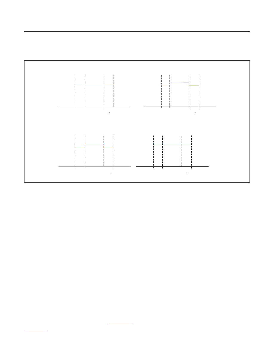
Thermistor Monitoring
The MAX14748 provides highly programmable thermal/
JEITA charge management. All thermal/JEITA charge
configuration parameters are set via the ThermCfg reg-
isters 0x1A - 0x1C. The charger is managed by thermal
information only if JEITACtrSet = 1.
The battery pack temperature is measured from a divider
formed by a pull-up resistor, an optional parallel resistor,
and the battery pack thermistor. When required, the pullup
resistor is connected to an internal supply through the
TPU input, and the voltage on the THM pin is compared to
an internal threshold. The supply voltage for the divider
is applied to the V
TPU
pin and may be connected to an
external supply or to V
CCINT
. The pullup resistor may
be complemented with an additional parallel resistor to
allow matching to different thermistor nominal values
and charging cutoff temperatures, T1, T2, T3, and T4.
There are two sets of cutoff temperatures optimized for
a thermistor with Beta = 3380 (0 °C/10 °C/45 °C/60 °C or
0 °C/10 °C/25 °C/45 °C) which can be selected as factory
default options. These cutoff temperatures divide the
temperature range into three zones, T1_T2, T2_T3, and
T3_T4. The charger is always turned off at temperatures
outside these zones when any thermal monitoring mode
is enabled. If the system needs to measure the THM
temperature when not charging, the internal pullup switch
may be enabled via the JeitaCfgR[1:0] bits.
Charging may be optionally disabled in the T1_T2 and
T3_T4 zones through the T_T_EnSet bits. The charge
current in each zone may be modified through T_T_
IFchg[2:0]. Battery-voltage termination reduction may also
be selectively applied through the T_T_VFset bits. See
MAX14748
USB Type-C Charger
www.maximintegrated.com
Maxim Integrated
29
Weak Battery Operation
The MAX14748 supports the weak battery provision of
the USB 2.0 specification. If an SDP adapter is detected
and the battery voltage is less than the precharge threshold,
the input current limit is set to 500mA and a 2-minute
timer starts. After the 2-minute timer expires, the input
current limit is set to zero. Any time during the 2-minute
countdown, the system may turn off the weak battery
state machine and assert control of the input current limit
by setting WeakBatEn to 0.
Battery Detection
The MAX14748 offers battery detection by detecting the presence
of the battery thermistor. If the thermistor is not present, THM
is pulled high by the external pullup resistor, and BatDet is set
to 0 indicating that the battery is not connected.
Integrated USB 2.0 Analog Switch
A high-speed USB switch is integrated to provide the
host data access to the connected USB device when an
SDP or CDP port is detected. The analog switch may
be controlled manually or automatically by configuring
the AnSwCntl[1:0] bits in register 0x2F. When the ana-
log switch control is set to the auto control setting then
the CDN/CDP pins are connected to TDN/TDP only
when a SDP or CDP port is detected. (See
for further details.)
SFOUT LDO
The SFOUT LDO is powered directly from the CHGIN
input and may be used to power a USB transceiver, or
as an indicator signal that a SDP/CDP port is present.
The LDO will operate with CHGIN voltages greater than
V
BDET
. The output voltage of SFOUT is selectable as
either 5V or 3.3V through the SfOutLvl bit, depending on
the system preference. SFOUT may be programmed to
turn on automatically when an SDP or CDP is detected,
or placed in manual mode and turned on through an I
2
C
command. This supply is always available when CHGIN
is present.
Internal Supplies and Regulators
The MAX14748 has two internal power supplies: V
CCINT
and BREG. V
CCINT
and BREG are always present when
CHGIN or BAT is present. These supplies share a common
source, but bypassed separately. The V
CCINT
and BREG
supplies require external bypass capacitors and are
regulated to a nominal value of 4.3V (typ).
Figure 6. Thermistor Monitoring
MAX14748
USB Type-C Charger
www.maximintegrated.com
Maxim Integrated
30
T
1
T
4
TEMPERATURE ( ºC)
CHARGING
NO
CHARGING
NO
CHARGING
T
2
T
3
I
PCHG
PREQUAL:
V
BAT
<
V
PCHG
T
1
T
4
TEMPERATURE ( ºC)
CHARGING
NO
CHARGING
NO
CHARGING
T
2
T
3
T1T2IFchg[2:0]
FAST CHARGE CONSTANT CURRENT:
V
PCHG
< V
BAT
< V
BATREG
T2T3IFchg[2:0]
T
1
T
4
TEMPERATURE ( ºC)
CHARGING
NO
CHARGING
T
2
T
3
V
BATREG
REGULATED VOLTAGE
NO
CHARGING
T
1
T
4
TEMPERATURE ( ºC)
CHARGING
NO
CHARGING
T
2
T
3
V
BATREG
REGULATED VOLTAGE
NO
CHARGING
V
BATREG
- 300mV
T3T4IFchg[2:0]
T1T2ENset =1, T3T4ENset = 1
T1T2VFset = 1, T3T4VFset = 1
T1T2ENset =1, T3T4ENset = 1
T1T2VFset = 0, T3T4VFset = 0
V
BATREG
- 300mV

Device Control Interface
While the MAX14748 is primarily controlled by I
2
C, GPIO
control is also offered for specific functions. The following
GPIO control signals are provided (note that these signals
only apply when CHGIN is present):
1) FSUS (Input): Force Suspend. This pin enables the
host microcontroller to force the input current limit to
zero. When CHGIN is present, a logic-high on the pin
causes the input OVP FET at CHGIN to open and the
input current to MAX14748 is reduced to less than
2mA. This pin has no effect if FSUSMsk = 1.
2) FLTIN (Input): Battery Fault Input. This pin allows
the system or battery pack to place the charger into
a fault condition using a GPIO pin. See Register
0x35 description for more details.
3) CDIR (Open-Drain Output): USB Superspeed MUX
control. In USB Type-C plug configurations, it is
necessary to detect the orientation of the connector
and route the Superspeed lines accordingly. The pin
can be used to automatically configure a USB Super-
speed MUX according to the orientation information
contained in the integrated Type-C detection block.
(This information is also available through I
2
C) The
CDIR output is pulled to GND when the CC1 pin is
active on the Type-C connector, otherwise it is high-
impedance.
4) SYSOK (Open-Drain Output): With CHGIN present,
the SYSOK output is asserted if the boost regulator
generates a V
SYS
greater than SYS UVLO threshold,
V
SYSUVLO
. Otherwise, the output is high-impedance.
This pin can be used as wake up the host system
from a dead-battery. Note that when V
SYS
falls
below the SYS UVLO falling threshold, the input
OVP switch is opened as the boost converter cannot
operate in this state.
5) BVCEN (Open-Drain Output): When CHGIN is
present and a Type-C device that requires V
CONN
is
found, this pin is asserted. This pin should be con-
nected to the enable pin of the V
CONN
power supply
enable. The output of BVCEN is push-pull between
GND and V
CCINT
.
System Faults
The MAX14748 monitors the system for faults including
OVP Soft Start Timeout, SYS UVLO, Direct Charging
Fault, Charger TImeout, Forced Charger Fault, Dead
Battery, CHGIN OVP.
b
for more details.
Table 1b. System Faults Summary
FAULT NAME
EFFECT
CAUSE DESCRIPTION
HOW TO RECOVER
STAUS BIT
OVP Soft-Start
TimeOut
System Fault Condition Latched.
OVP/Boost/Charger Off
UFP: V
BYP
is not within
50mV of V
CHGIN
at Soft Start
TimeOut (100ms typ)
Unplug/Replug Type-C
cable or reset device via
USBCRSet of Reg 0x30
SysFlt
(Reg 0x02)
SYS UVLO
System Fault Condition Latched.
OVP/Boost/Charger Off
UFP: V
SYS
falls below SYS
UVLO threshold while in Boost
mode or V
SYS
fails to reach
above SYS UVLO threshold
within 20ms after V
BYP
rises
Unplug/Replug Type-C
cable or resert device via
USBCRSet of Reg 0x30
SysFlt
(Reg 0x02)
Direct
Charging Fault
Charger Fault Condition
Latched. Charger Off
UFP: V
BAT
falls below V
PCHG
while in Fast Charge mode
Cycle ChgEn or treat as
System Fault
DirChgFault
(Reg 0x05)
Charger
Timeout
Charger Fault Condition
Latched. Charger Off
UFP: Pre-charge or Fast-
charge Timer expires
Cycle ChgEn or treat as
System Fault
ChgStat[3:0]
(Reg 0x05)
Forced
Charger Fault
Charger Off
UFP: Logic-low applied on
FLTIN pin
Logic-high applied on
FLTIN pin
ChgStat[3:0]
(Reg 0x05)
Dead Battery
System Fault Condition Latched.
OVP/Boost/Charger Off
UFP: DeadBattery detection
enabled and SDP detected:
V
BAT
fails to reach above
V
PCHG
within 2min
Treat as System Fault or
disable DeadBattery
WbChg
(Reg 0x02)
CHGIN OVP
OVP/Boost/Charger OFF
V
CHGIN
rises above V
OVP
Reduce V
CHGIN
below
V
OVP_F
ChginOVP
(Reg 0x02)
MAX14748
USB Type-C Charger
www.maximintegrated.com
Maxim Integrated
31
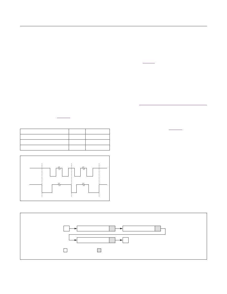
I
2
C Interface
The MAX14748 contain an I
2
C-compatible interface for
data communication with a host controller (SCL and
SDA). The interface supports a clock frequency of up to
400kHz. SCL and SDA require pullup resistors that are
connected to a positive supply.
Start, Stop, And Repeated Start Conditions
When writing to the MAX14748 using I
2
C, the master
sends a START condition (S) followed by the MAX14748
I
2
C address. After the address, the master sends the
register address of the register that is to be programmed.
The master then ends communication by issuing a
STOP condition (P) to relinquish control of the bus, or
a REPEATED START condition (Sr) to communicate to
another I
2
C slave. See
.
Slave Address
Set the Read/Write bit high to configure the MAX14748
to read mode (
Set the Read/Write bit low to
configure the MAX14748 to write mode. The address is
the first byte of information sent to the MAX14748 after
the START condition.
Bit Transfer
One data bit is transferred on the rising edge of each SCL
clock cycle. The data on SDA must remain stable during
the high period of the SCL clock pulse. Changes in SDA
while SCL is high and stable are considered control sig-
nals (see the
section). Both SDA and SCL remain high when the bus is
not active.
Single-Byte Write
In this operation, the master sends an address and two
data bytes to the slave device (
following
procedure describes the single byte write operation:
1) The master sends a START condition
2) The master sends the 7-bit slave address plus a
write bit (low)
3) The addressed slave asserts an ACK on the data line
4) The master sends the 8-bit register address
5) The slave asserts an ACK on the data line only if the
address is valid (NAK if not)
6) The master sends 8 data bits
7) The slave asserts an ACK on the data line
8) The master generates a STOP condition
Table 2. I
2
C Slave Addresses
Figure 7. I
2
C START, STOP and REPEATED START Conditions
Figure 8. Write Byte Sequence
ADDRESS FORMAT
HEX
BINARY
7-Bit Slave ID
0x0A
0001010
Write Address
0x14
00010100
Read Address
0x15
00010101
MAX14748
USB Type-C Charger
www.maximintegrated.com
Maxim Integrated
32
SCL
SDA
S
Sr
P
S
P
DEVICE SLAVE ADDRESS - W A
8 DATA BITS
WRITE SINGLE BYTE
FROM MASTER TO SLAVE
FROM SLAVE TO MASTER
A
REGISTER ADDRESS
A
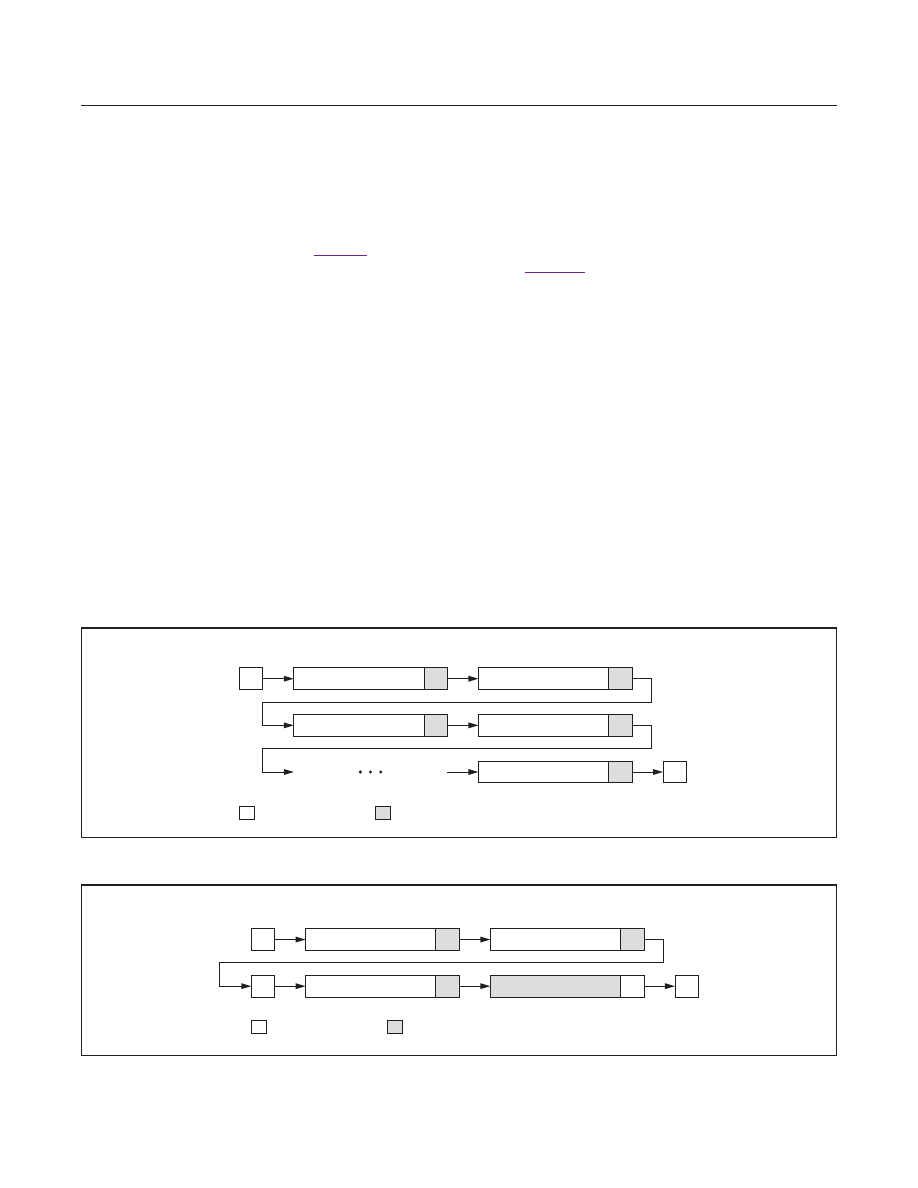
Burst Write
In this operation, the master sends an address and mul-
tiple data bytes to the slave device (
The slave
device automatically increments the register address after
each data byte is sent. The following procedure describes
the burst write operation:
1) The master sends a START condition.
2) The master sends the 7-bit slave address plus a
write bit (low).
3) The addressed slave asserts an ACK on the data line.
4) The master sends the 8-bit register address.
5) The slave asserts an ACK on the data line only if the
address is valid (NAK if not).
6) The master sends eight data bits.
7) The slave asserts an ACK on the data line.
8) Repeat 6 and 7 N-1 times.
9) The master generates a STOP condition.
Single-Byte Read
In this operation, the master sends an address plus two
data bytes and receives one data byte from the slave
device (
The following procedure describes the
single byte read operation:
1) The master sends a START condition.
2) The master sends the 7-bit slave address plus a
write bit (low).
3) The addressed slave asserts an ACK on the data line.
4) The master sends the 8-bit register address.
5) The slave asserts an ACK on the data line only if the
address is valid (NAK if not).
6) The master sends a REPEATED START condition.
7) The master sends the 7-bit slave address plus a
read bit (high).
8) The addressed slave asserts an ACK on the data line.
9) The slave sends eight data bits.
10) The master asserts a NACK on the data line.
11) The master generates a STOP condition.
Figure 9. Burst Write Sequence
Figure 10. Read Byte Sequence
MAX14748
USB Type-C Charger
www.maximintegrated.com
Maxim Integrated
33
S
DEVICE SLAVE ADDRESS - W A
8 DATA BITS - 1
BURST WRITE
A
REGISTER ADDRESS
A
8 DATA BITS - N
A
8 DATA BITS - 2
A
FROM MASTER TO SLAVE
FROM SLAVE TO MASTER
P
S
Sr
DEVICE SLAVE ADDRESS - W A
DEVICE SLAVE ADDRESS - R
READ SINGLE BYTE
A
REGISTER ADDRESS
A
8 DATA BITS
NA
FROM MASTER TO SLAVE
FROM SLAVE TO MASTER
P
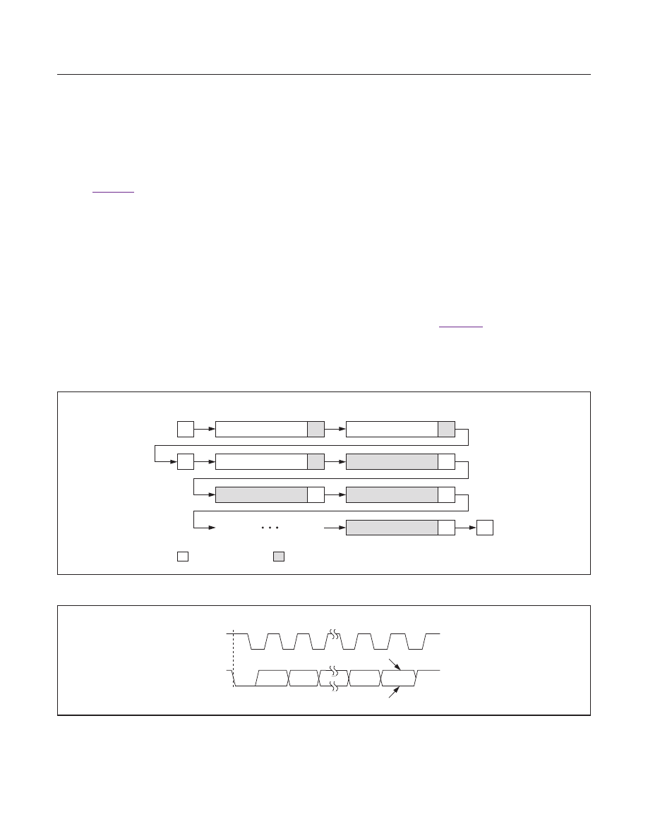
Burst Read
In this operation, the master sends an address plus two
data bytes and receives multiple data bytes from the slave
device (
The following procedure describes the
burst byte read operation:
1) The master sends a START condition.
2) The master sends the 7-bit slave address plus a
write bit (low).
3) The addressed slave asserts an ACK on the data line.
4) The master sends the 8-bit register address.
5) The slave asserts an ACK on the data line only if the
address is valid (NAK if not).
6) The master sends a REPEATED START condition.
7) The master sends the 7-bit slave address plus a
read bit (high).
8) The slave asserts an ACK on the data line.
9) The slave sends eight data bits.
10) The master asserts an ACK on the data line.
11) Repeat 9 and 10 N-2 times.
12) The slave sends the last eight data bits.
13) The master asserts a NACK on the data line.
14) The master generates a STOP condition.
Acknowledge Bits
Data transfers are acknowledged with an acknowledge bit
(ACK) or a not-acknowledge bit (NACK). Both the master
and the MAX14748 generate ACK bits. To generate an
ACK, pull SDA low before the rising edge of the ninth
clock pulse and hold it low during the high period of the
ninth clock
To generate a NACK,
leave SDA high before the rising edge of the ninth clock
pulse and leave it high for the duration of the ninth clock
pulse. Monitoring for NACK bits allows for detection of
unsuccessful data transfers.
Figure 11. Burst Read Sequence
Figure 12. Acknowledge
MAX14748
USB Type-C Charger
www.maximintegrated.com
Maxim Integrated
34
S
Sr
DEVICE SLAVE ADDRESS - W A
DEVICE SLAVE ADDRESS - R
BURST READ
A
REGISTER ADDRESS
A
8 DATA BITS - 1
A
A
8 DATA BITS - 3
8 DATA BITS - 2
A
8 DATA BITS - N
NA
FROM MASTER TO SLAVE
FROM SLAVE TO MASTER
P
NOT ACKNOWLEDGE
ACKNOWLEDGE
1
2
8
9
SDA
SCL
S

Table 3. I2C Register Map
REGISTER
ADDRESS
REGISTER
NAME
R/W
B7
B6
B5
B4
B3
B2
B1
B0
0x00
ChipID
R
ChipId[7:0]
0x01
ChipRev
R
ChipRevH[3:0]
ChipRevL[3:0]
0x02
DevStatus1
R
SysFlt
ChgInOVP
ILim
VSysReg
ThrmSd150
ThrmSd120
BatDet
WbChg
0x03
AICLStatus
R
AICLStatus[2:0]
AICLCurSet[4:0]
0x04
DevStatus2
R
-
BattPREQB
BattUVLOB
BypUVLO
SysUVLOB
DCDCILim
DCDCRunA
way
DCDCPGood
0x05
ChgStatus
R
DirChgFault
-
LowPow
-
ChgStat[3:0]
0x06
JEIT
AStatus
R
-
-
-
ChgThrmRegCur
ChgThrmRegVlt
ChgThrmStat[2:0]
0x07
BCStatus
R
VBUSDet
ChgT
ypRun
PrChgT
yp[2:0]
DCDTmo
ChgT
yp[1:0]
0x08
Reserved
R
-
-
-
-
-
-
-
-
0x09
CCStatus1
R
CCPinStat[1:0]
CCIStat[1:0]
CCVcnStat
CCStat[2:0]
0x0A
CCStatus2
R
-
-
-
-
VSAFE0V
DetAbrt
-
-
0x0B
DevInt1
COR
SysFltI
ChgInOVPI
ILimI
VSysRegI
ThrmSd150I
ThrmSd120I
BatDetI
WbChgI
0x0C
AICLInt
COR
-
AICLI
-
-
-
-
-
-
0x0D
DevInt2
COR
-
BattPREQi
BattUVLOI
BypUVLOI
SysUVLOI
-
-
DCDCPGoodI
0x0E
ChgInt
COR
DirChgFaultI
LowPowRI
LowPowFI
-
-
-
-
ChgStatI
0x0F
JEIT
AInt
COR
-
-
-
ChgThrmRegCurI
ChgThrmRegVltI
-
-
ChgThrmStatI
0x10
BCInt
COR
VBUSDetI
-
-
ChgT
ypRunFI
ChgT
ypRunRI
PrChgT
ypI
DCDTmoI
ChgT
ypI
0x1
1
CCInt
COR
-
VSAFE0VI
DetAbrtI
CCPinStatI
CCIStatI
CCVcnStatI
CCStatI
0x12
DevInt1Mask
R/W
SysFltIM
ChgInOVPIM
ILimIM
VSysRegIM
ThrmSd150IM
ThrmSd120IM
BatDetIM
WbChgIM
0x13
AICLIntMask
R/W
-
AICLIM
-
-
-
-
-
-
0x14
DevInt2Mask
R/W
-
BattPREQIM
BattUVLOIM
BypUVLOIM
SysUVLOIM
DCDCILimIM
DCDCRunA
wayIM
DCDCPGoodIM
0x15
ChgIntMask
R/W
DirChgFaultIM
LowPowRIM
LowPowFIM
-
-
-
-
ChgStatIM
0x16
JEIT
AIntMask
R/W
-
-
-
ChgThrmReg
CurIM
ChgThrmReg
VltIM
-
-
ChgThrmStatIM
0x17
BCIntMask
R/W
VBUSDetIM
-
-
ChgT
ypRunFIM
ChgT
ypRunRIM
PrChgT
ypIM
DCDTmoIM
ChgT
ypIM
0x18
CCIntMask
R/W
-
VSAFE0VIM
DetAbrtIM
-
CCPinStatIM
CCIStatIM
CCVcnStatIM
CCStatIM
0x19
LED_CTRL
R/W
-
-
-
-
-
-
LEDCtrl
LEDManual
0x1A
ThermaCfg1
R/W
T1T2IFchg[2:0]
T2T3IFchg[2:0]
JeitaCfgR[1:0]
0x1B
ThermaCfg2
R/W
T3T4IFchg[2:0]
-
T3T4ENset
T1T2ENset
T3T4VFset
T1T2VFset
0x1C
ThermaCfg3
R/W
-
-
-
-
-
-
JEIT
ACtrSet
W
armCoolSel*
0x1D
ChargerCtrl1
R/W**
ChgAutoStp
BatReChg[1:0]
-
-
BatReg[1:0]
ChgEn
0x1E
ChargerCtrl2
R/W**
-
VPchg[2:0]
IPChg[1:0]
ChgDone[1:0]
MAX14748
USB Type-C Charger
www.maximintegrated.com
Maxim Integrated
35

Table
3.
I2C
Register
Map
(continued)
Note :
COR = Clear-o
n-read
* Read Only
** Read
Only if W
riteProtect is enabled
(See
).
Reserved bits must not be modified from their default states to ensure proper operation.
REGISTER
ADDRESS
REGISTER
NAME
R/W
B7
B6
B5
B4
B3
B2
B1
B0
0x1F
ChargerCtrl3
R/W**
-
ChgAutoSta
MtChgTmr[1:0]
FChgTmr[1:0]
PChgTmr[1:0]
0x20
ChargerCtrl4
R/W**
W
eakBatStat[2:0]*
-
-
W
eakBatEn
-
-
0x21
CurLimCtrl
R/W
CurLim1Frc
FSUSMsk
CurLim1Set[4:0]
0x22
CurLimStatus
R
CurLim2Rb[2:0]
SpvChgILim[4:0]
0x23
BBCFG1
R/W**
BoostRComp[3:0]
-
-
-
-
0x24
BBCFG2
R/W**
-
-
-
BBFrcZX
BuckVSet[3:0]
0x25
BCCtrl1
R/W
DCD2s
SfOutLvl
-
ADC3PDet
SfOutCtrl[1:0]
ChgDetMan
ChgDetEn
0x26
Reserved
R
-
-
-
-
-
-
-
-
0x27
CCCtrl1
R/W
-
-
-
-
CCSnkSrc
CCDbgEn
CCAudEn
CCDetEn
0x28
CCCtrl2
R/W
CCForceError
SnkAttached
Lock
CCSnkSrcSwp
CCSrcSnkSwp
CCVcnSwp
CCVcnEn
CCSrcRst
CCSnkRst
0x29
CCCtrl3
R/W
-
-
-
-
CCT
rySnk
CCPreferSnk
CCDRPPhase[1]
CCDRPPhase[0]
0x2A
CHGINILim1
R
-
CHGINILim[6:0]
0x2B
CHGINILim2
R/W
-
-
-
-
CHGINILimGate
SDPMaxCur[1:0]
CDPMaxCur
0x2C
AICLCFG1
R/W
AICLEn
-
-
-
-
AICLAbort
0x2D
AICLCFG2
R/W
BYPUVLO[2:0]
AICLMaxI[4:0]
0x2E
AICLCFG3
R/W
-
-
-
BYPDeb
AICL
TBlk[1:0]
AICL
TStep[1:0]
0x2F
DPDNSw
R/W
-
-
-
-
-
-
AnSwCntl[1:0]
0x30
Others
R/W
-
-
-
-
-
-
-
USBCRset
0x31
Reserved
R
-
-
-
-
-
-
-
-
0x32
Reserved
R
-
-
-
-
-
-
-
-
0x33
LowPow
R/W
LowPowEn
-
-
-
-
-
-
LowPowAbort
0x34
Reserved
R
-
-
-
-
-
-
-
-
0x35
FL
TSel
R/W
FL
TSelect[1:0]
-
-
-
-
-
-
MAX14748
USB Type-C Charger
www.maximintegrated.com
Maxim Integrated
36
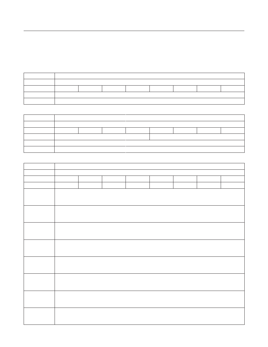
Table 4. ChipID Register (0x00)
Table 5. ChipRev Register (0x01)
Table 6. DevStatus1 Register (0x02)
ADDRESS:
0x00
MODE:
Read Only
BIT
7
6
5
4
3
2
1
0
NAME
ChipId[7:0]
ChipId[7:0]
ChipId[7:0] bits show information about the version of the MAX14748.
ADDRESS:
0x01
MODE:
Read Only
BIT
7
6
5
4
3
2
1
0
NAME
ChipRevH[3:0]
ChipRevL[3:0]
ChipRevH[3:0] ChipRevH[3:0] bits show information about the revision of the MAX14748 silicon.
ChipRevL[3:0]
ChipRevL[3:0] bits show information about the revision of the MAX14748 silicon.
ADDRESS:
0x02
MODE:
Read Only
BIT
7
6
5
4
3
2
1
0
NAME
SysFlt
ChgInOVP
ILim
VSysReg
ThrmSd150
ThrmSd120
BatDet
WbChg
SysFlt
System Fault
0 = System voltage is normal
1 = SYS voltage below SYS UVLO Threshold and the condition latched.
ChgInOVP
CHGIN Overvoltage Protection Flag
0 = CHGIN OVP not active
1 = CHGIN OVP active
ILim
Input Current Limiting
0 = CHGIN input current within limit
1 = CHGIN input in current limit
VSysReg
SYS Regulation (SYSOK)
0 = SYS voltage above SYS UVLO threshold and boost regulating SYS
1 = SYS voltage below SYS UVLO threshold or Boost not regulating SYS
ThrmSd150
Thermal shutdown
0 = Device in normal operation Mode
1 = Device in thermal shutdown (T
DIE
> 150 °C)
ThrmSd120
Thermal Warm
0 = Device in normal operation Mode
1 = 120 °C < T
DIE
< 150 °C
BatDet
Status of Battery Detection
0 = No battery detected
1 = Battery detected
WbChg
Weak Battery Charging
0 = Weak Battery Charge Timer expired or not running
1 = Weak Battery Charge Timer running
MAX14748
USB Type-C Charger
www.maximintegrated.com
Maxim Integrated
37
I
2
C Register Descriptions
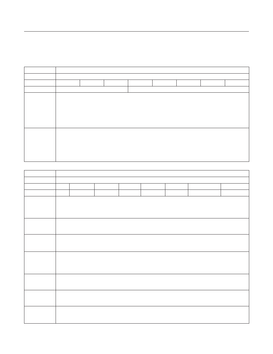
Table 7. AICLStatus Register (0x03)
Table 8. DevStatus2 Register (0x04)
ADDRESS:
0x03
MODE:
Read Only
BIT
7
6
5
4
3
2
1
0
NAME
AICLStatus[2:0]
AICLCurSet[4:0]
AICLStatus[2:0]
AICL Status
000 = AICL Off
001 = AICL Precheck
010 = AICL Increment
011 = AICL Blank
100 = AICL Idle
101 = AICL No Connection
AICLCurSet[4:0]
Current limit set by AICL (if active)
0 = 100mA
1 = 200mA
¦
30 = 3.1A
31 = 3.2A
ADDRESS:
0x04
MODE:
Read Only
BIT
7
6
5
4
3
2
1
0
NAME
-
BattPREQB BattUVLOB BypUVLO
SysUVLOB
DCDCILim
DCDCRunAway
DCDCPGood
BattPREQB
V
BAT
vs. V
PCHG
(V
PCHG
programmable from 5.7V to 6.4V, BattPreqB status is NOT valid while the Weak
Battery 2min timer is running.)
0 = V
BAT
below V
PCHG
threshold
1 = V
BAT
above V
PCHG
threshold
BattUVLOB
V
BAT
vs. V
BATUVLO
(BattUVLOB status is only valid in boost mode with CHGIN present.)
0 = V
BAT
below V
BATUVLO
threshold
1 = V
BAT
above V
BATUVLO
threshold
BypUVLO
V
BYP
vs. V
BYPUVLO
(V
BYPUVLO
programmable from 3.8V to 4.5V)
0 = V
BYP
above V
BYPUVLO
theshold
1 = V
BYP
below V
BYPUVLO
theshold
SysUVLOB
V
SYS
vs. V
SYSUVLO
(V
SYSUVLO
programmable from 6.1V to 6.8V, SysUVLOB status is only valid in boost
mode with CHGIN present))
0 = V
SYS
below V
SYSUVLO
threshold
1 = V
SYS
above V
SYSUVLO
threshold
DCDCILim
Reverse Buck Converter Current Limit Status
0 = Normal Operation
1 = Buck current limit has been reached
DCDCRunAway
Reverse Buck Converter Runaway Status
0 = Normal Operation
1 = Buck runaway is asserted
DCDCPGood
Reverse Buck Converter Regulation Status
0 = Buck regulated value below 82% of the target value
1 = Normal operation
MAX14748
USB Type-C Charger
www.maximintegrated.com
Maxim Integrated
38
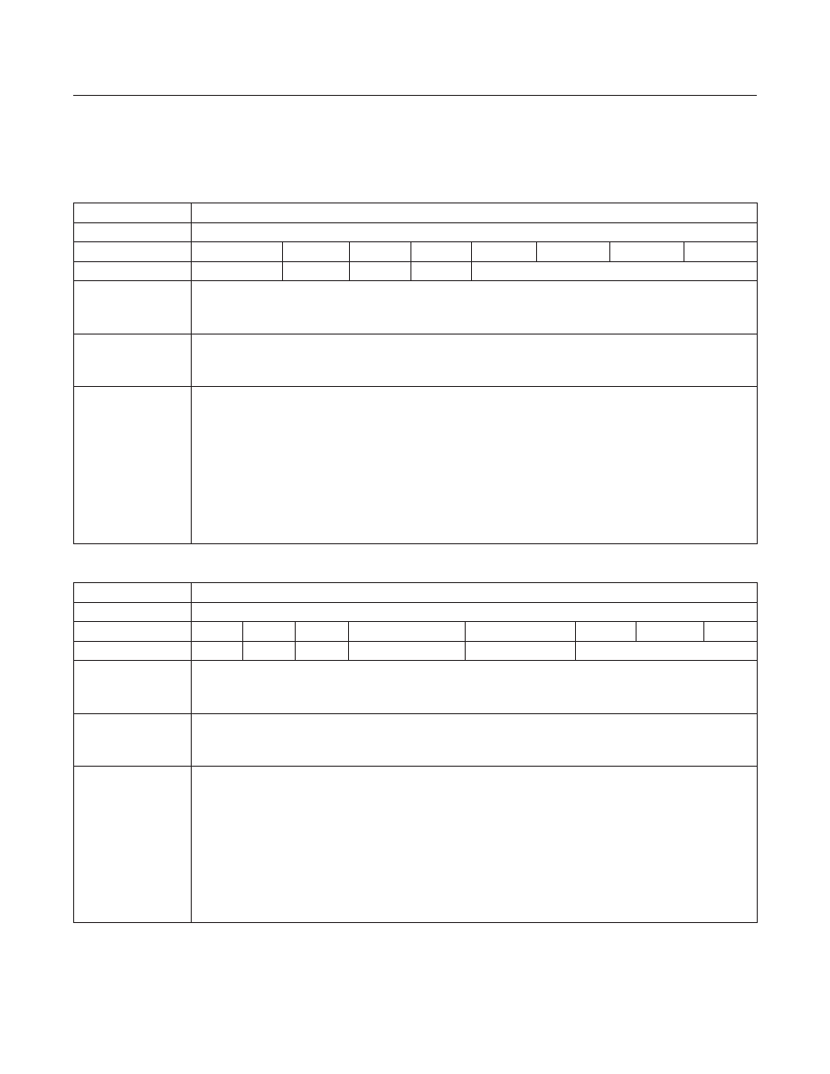
Table 9. ChgStatus Register (0x05)
Table 10. JEITAStatus Register (0x06)
ADDRESS:
0x05
MODE:
Read Only
BIT
7
6
5
4
3
2
1
0
NAME
DirChgFault
-
LowPow
-
ChgStat[3:0]
DirChgFault
Direct charging fault
0 = Device in normal operation
1 = V
BAT
drops below V
PCHG
when battery is in supplement mode.
LowPow
Low Power Mode
0 = Not In Low Power Mode
1 = In Low Power Mode
ChgStat[3:0]
Status of Charger Mode
0000 = Charger off
0001 = Charging suspended due to temperature (see state diagram)
0010 = Pre-charge in progress
0011 = Fast-charge, constant current mode in progress
0100 = Fast-charge, constant voltage mode in progress
0101 = Maintain charge in progress
0110 = Maintain charge done
0111 = Charger fault condition (see state diagram)
1000 = Battery Fault Suspend (see state diagram)
ADDRESS:
0x06
MODE:
Read Only
BIT
7
6
5
4
3
2
1
0
NAME
-
-
-
ChgThrmRegCur
ChgThrmRegVlt
ChgThrmStat[2:0]
ChgThrmRegCur
FastCharge Current reduced due to JEITA status
0 = Not changed
1 = Reduced
ChgThrmRegVlt
Battery Regulation Voltage reduced due to JEITA status
0 = Not Changed
1 = Reduced
ChgThrmStat[2:0]
Thermistor Monitor
000 = T < T1
001 = T1 < T < T2
010 = T2 < T < T3
011 = T3 < T < T4
100 = T > T4
101 = No thermistor detected (THM high due to external pullup). Note: If a parallel resistor is used for
thermistor monitoring, this mode may not function properly.
110 = NTC input disabled through ThermEn.
111 = Detection disabled due to CHGIN not present.
MAX14748
USB Type-C Charger
www.maximintegrated.com
Maxim Integrated
39
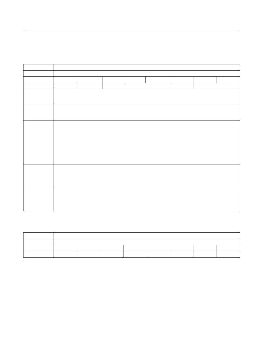
Table 11. BCStatus Register (0x07)
Table 12. Reserved Register (0x08)
ADDRESS:
0x09
MODE:
Read Only
BIT
7
6
5
4
3
2
1
0
NAME
VBUSDet
ChgTypRun
PrChgTyp[2:0]
DCDTmo
ChgTyp[1:0]
VBUSDet
Status of CHGIN Detection
0 = V
CHGIN
< V
BDET
1 = V
CHGIN
> V
BDET
ChgTypRun
Charger Detection Running Status
0 = Not Running
1 = Running
PrChgTyp[2:0]
Output of Proprietary Charger Detection
000 = Unknown
001 = Samsung 2A
010 = Apple 0.5A
011 = Apple 1A
100 = Apple 2A
101 = Apple 12W
110 = 3A DCP (If enabled)
111 = RFU
DCDTmo
DCD Time Out. DCD detection timed out during charger detection, indicating D+/D- are open. BC1.2 detection
continues as required by BC1.2, but SDP most likely is found.
0 = No Timeout or detection not run
1 = DCD Timeout occurred
ChgTyp[1:0]
Output of Charger Detection
00 = Nothing attached
01 = SDP, USB Cable attached
10 = CDP, Charging Downstream Port (current depends on USB operating speed)
11 = DCP, Dedicated Charger (current up to 1.5A)
ADDRESS:
0x08
MODE:
Read Only
BIT
7
6
5
4
3
2
1
0
NAME
-
-
-
-
-
-
-
-
MAX14748
USB Type-C Charger
www.maximintegrated.com
Maxim Integrated
40
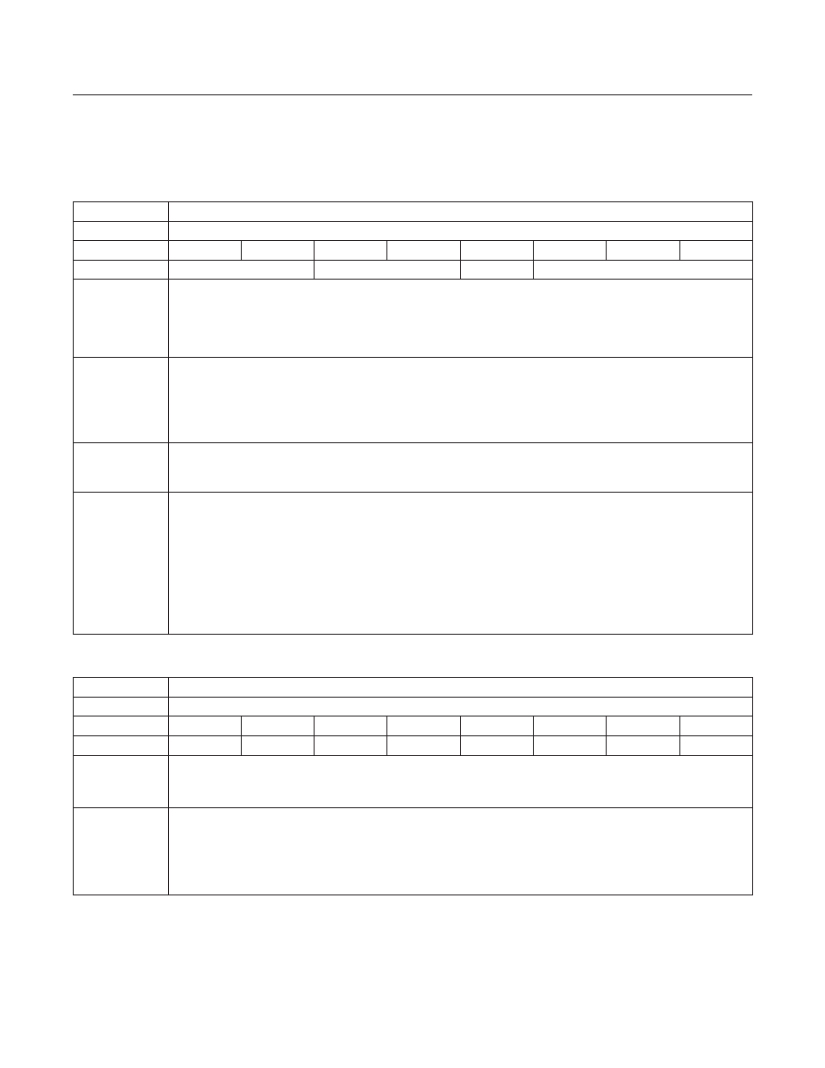
Table 13. CCStatus1 Register (0x09)
Table 14. CCStatus2 Register (0x0A)
ADDRESS:
0x09
MODE:
Read Only
BIT
7
6
5
4
3
2
1
0
NAME
CCPinStat[1:0]
CCIStat
CCVcnStat
CCStat[2:0]
CCPinStat[1:0]
Status of Active CC Pin
00 = No Determination
01 = CC1 Active
10 = CC2 Active
11 = RFU
CCIStat
CC Pin Detected Allowed VBUS Current in UFP mode
00 = Not in UFP mode
01 = 500mA
10 = 1.5A
11 = 3.0A
CCVcnStat
Status of VCONN Output
0 = VCONN Disabled
1 = VCONN Enabled
CCStat[2:0]
Output of CC Pin Detection State Machine
000 = No Connection
001 = UFP
010 = DFP
011 = Audio Accessory
100 = Debug Accessory
101 = Error
110 = Disabled
111 = RFU
ADDRESS:
0x0A
MODE:
Read Only
BIT
7
6
5
4
3
2
1
0
NAME
-
-
-
-
VSAFE0V
DetAbrt
-
-
VSAFE0V
Status of VBUS Detection. (Valid only in Attached.SRC_CCx, Attached.SNK_CCx state)
0 = V
CHGIN
< VSAFE0V
1 = V
CHGIN
> VSAFE0V
DetAbrt
Charger Detection Abort
0 = Charger Detection runs if ChgDetEn = 1 and VBUS is valid for the debounce time
1 = Charger Detection is aborted by Type-C State Machine. Charger detection will run if ChgDetEn = 1 and
VBUS is valid for the debounce time. ChgDetMan bit allows manual run of charger detection. If Charger
Detection is in progress, DetAbrt = 1 immediately stops the in-progress detection.
MAX14748
USB Type-C Charger
www.maximintegrated.com
Maxim Integrated
41
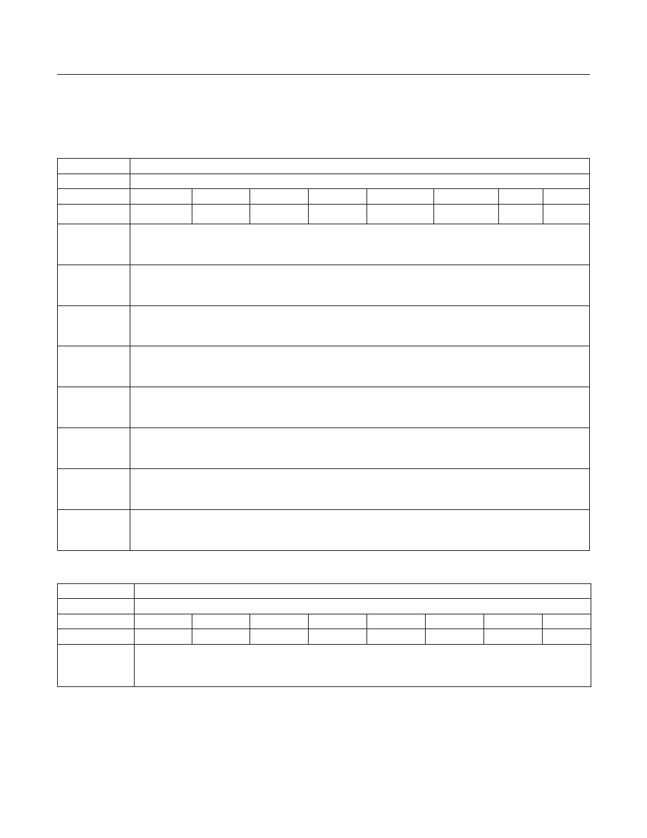
Table 15. DevInt1 Register (0x0B)
Table 16. AICLInt Register (0x0C)
ADDRESS:
0x0B
MODE:
Clear On Read
BIT
7
6
5
4
3
2
1
0
NAME
SysFltI
ChgInOVPI
ILimI
VSysRegI
ThrmSd150I
ThrmSd120I
BatDetI
WbChgI
SysFltI
SysFlt status change interrupt.
0 = Status of SysFlt has NOT changed since the last time SysFltI was read
1 = Status of SysFlt has changed since the last time SysFltI was read
ChgInOVPI
ChgInOVP status change interrupt.
0 = Status of ChgInOVP has NOT changed since the last time ChgInOVPI was read
1 = Status of ChgInOVP has changed since the last time ChgInOVPI was read
ILimI
ILim status change interrupt.
0 = Status of ILim has NOT changed since the last time ILimI was read
1 = Status of ILim has changed since the last time ILimI was read
VSysRegI
VSysReg status change interrupt.
0 = Status of VSysReg has NOT changed since the last time VSysRegI was read
1 = Status of VSysReg has changed since the last time VSysRegI was read
ThrmSd150I
ThrmSd150 status change interrupt.
0 = Status of ThrmSd150 has NOT changed since the last time ThrmSd150I was read
1 = Status of ThrmSd150 has changed since the last time ThrmSd150I was read
ThrmSd120I
ThrmSd120 status change interrupt.
0 = Status of ThrmSd120 has NOT changed since the last time ThrmSd120I was read
1 = Status of ThrmSd120 has changed since the last time ThrmSd120I was read
BatDetI
BatDet status change interrupt.
0 = Status of BatDet has NOT changed since the last time BatDetI was read
1 = Status of BatDet has changed since the last time BatDetI was read
WbChgI
WbChg status change interrupt.
0 = Status of WbChg has NOT changed since the last time WbChgI was read
1 = Status of WbChg has changed since the last time WbChgI was read
ADDRESS:
0x0C
MODE:
Clear On Read
BIT
7
6
5
4
3
2
1
0
NAME
-
AICLI
-
-
-
-
-
-
AICLI
AICLStatus status change interrupt.
0 = Status of AICLStatus has NOT changed since the last time AICLI was read
1 = Status of AICLStatus has changed since the last time AICLI was read
MAX14748
USB Type-C Charger
www.maximintegrated.com
Maxim Integrated
42
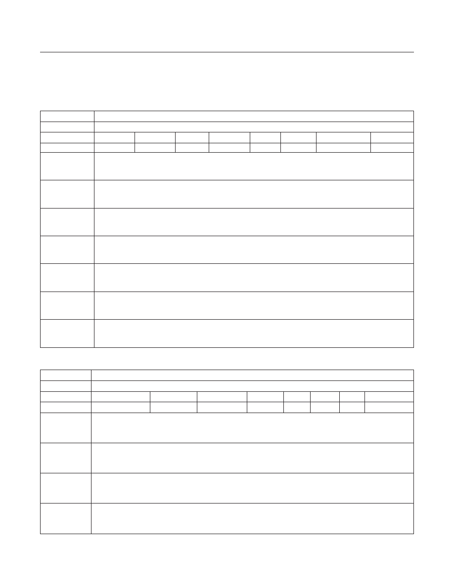
Table 17. DevInt2 Register (0x0D)
Table 18. ChgInt Register (0x0E)
ADDRESS:
0x0D
MODE:
Clear On Read
BIT
7
6
5
4
3
2
1
0
NAME
-
BattPREQI BattUVLOI BypUVLOI SysUVLOI DCDCILimI DCDCRunAwayI DCDCPGoodI
BattPREQI
BattPREQ status change interrupt.
0 = Status of BattPREQ has NOT changed since the last time BattPREQI was read
1 = Status of BattPREQ has changed since the last time BattPREQI was read
BattUVLOI
BattUVLO status change interrupt.
0 = Status of BattUVLO has NOT changed since the last time BattUVLOI was read
1 = Status of BattUVLO has changed since the last time BattUVLOI was read
BypUVLOI
BypUVLO status change interrupt.
0 = Status of BypUVLO has NOT changed since the last time BypUVLOI was read
1 = Status of BypUVLO has changed since the last time BypUVLOI was read
SysUVLOI
SysUVLO status change interrupt.
0 = Status of SysUVLO has NOT changed since the last time SysUVLOI was read
1 = Status of SysUVLO has changed since the last time SysUVLOI was read
DCDCILimI
DCDCILim status change interrupt.
0 = Status of DCDCILim has NOT changed since the last time DCDCILim was read
1 = Status of DCDCILim has changed since the last time DCDCILim was read
DCDCRunAwayI
DCDCRunAway status change interrupt.
0 = Status of DCDCRunAway has NOT changed since the last time DCDCRunAway was read
1 = Status of DCDCRunAway has changed since the last time DCDCRunAway was read
DCDCPGoodI
DCDCPGood status change interrupt.
0 = Status of DCDCPGood has NOT changed since the last time DCDCPGoodI was read
1 = Status of DCDCPGood has changed since the last time DCDCPGoodI was read
ADDRESS:
0x0E
MODE:
Clear On Read
BIT
7
6
5
4
3
2
1
0
NAME
DirChgFaultI
LowPowRI
LowPowFI
-
-
-
-
ChgStatI
DirChgFaultI
DirChgFault status change interrupt.
0 = Status of DirChgFault has NOT changed since the last time DirChgFaultI was read
1 = Status of DirChgFault has changed since the last time DirChgFaultI was read
LowPowRI
LowPow Rising Edge interrupt.
0 = LowPow bit rise edge has NOT occurred since the last time LowPowRI was read
1 = LowPow bit rise edge has occurred since the last time LowPowRI was read
LowPowFI
LowPow Falling Edge interrupt.
0 = LowPow bit falling edge has NOT occurred since the last time LowPowFI was read
1 = LowPow bit falling edge has occurred since the last time LowPowFI was read
ChgStatI
ChgStat[3:0] status change interrupt.
0 = Status of ChgStat[3:0] has NOT changed since the last time ChgStatI was read
1 = Status of ChgStat[3:0] has changed since the last time ChgStatI was read
MAX14748
USB Type-C Charger
www.maximintegrated.com
Maxim Integrated
43
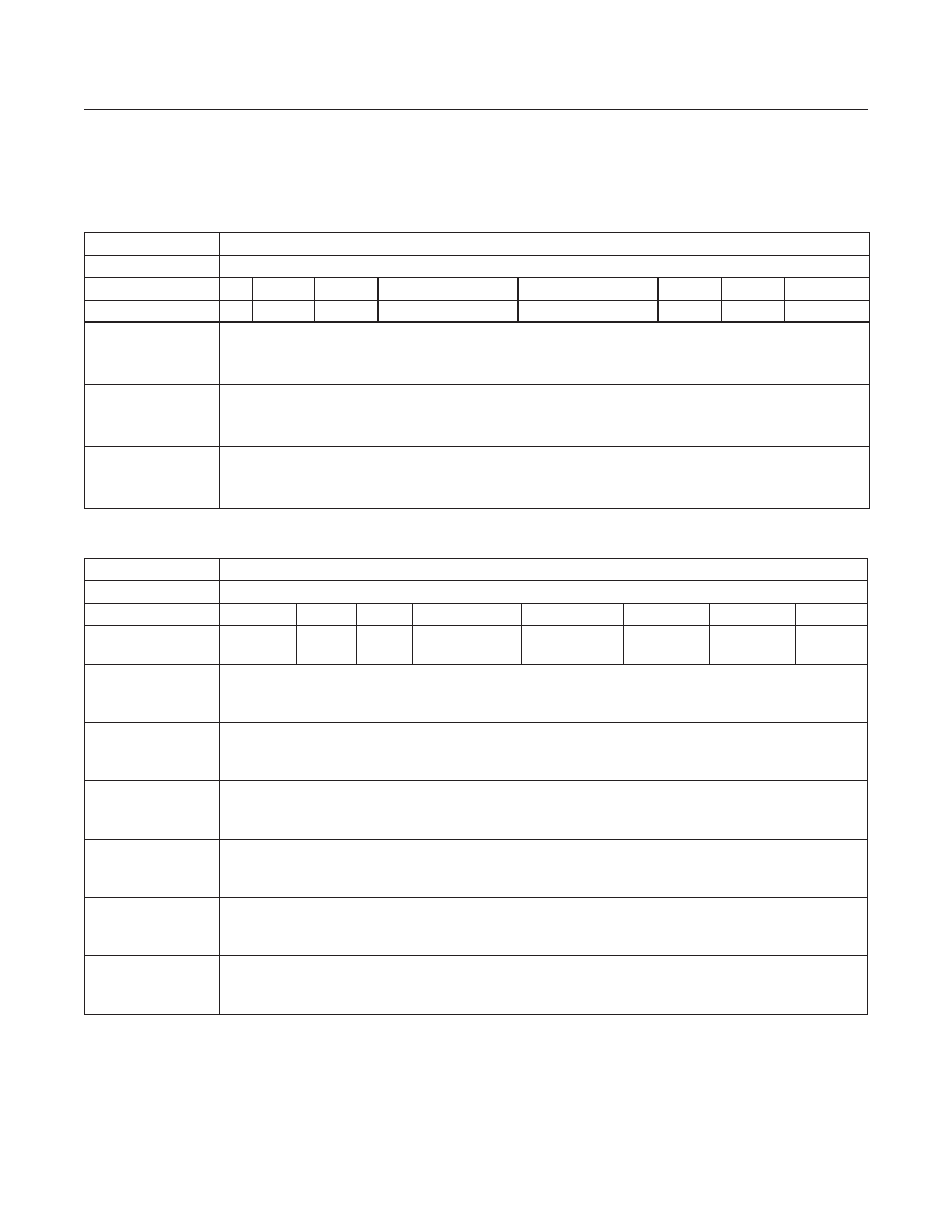
Table 19. JEITAInt Register (0x0F)
Table 20. BCInt Register (0x10)
ADDRESS:
0x0F
MODE:
Clear On Read
BIT
7
6
5
4
3
2
1
0
NAME
-
-
-
ChgThrmRegCurI
ChgThrmRegVltI
-
-
ChgThrmI
ChgThrmRegCurI
ChgThrmRegCur status change interrupt.
0 = Status of ChgThrmRegCur has NOT changed since the last time ChgThrmRegCurI was read
1 = Status of ChgThrmRegCur has changed since the last time ChgThrmRegCurI was read
ChgThrmRegVltI
ChgThrmRegVlt status change interrupt.
0 = Status of ChgThrmRegVlt has NOT changed since the last time ChgThrmRegVltI was read
1 = Status of ChgThrmRegVlt has changed since the last time ChgThrmRegVltI was read
ChgThrmStatI
ChgThrmStat[2:0] status change interrupt.
0 = Status of ChgThrmStat[2:0] has NOT changed since the last time ChgThrmStatI was read
1 = Status of ChgThrmStat[2:0] has changed since the last time ChgThrmStatI was read
ADDRESS:
0x10
MODE:
Clear On Read
BIT
7
6
5
4
3
2
1
0
NAME
VBUSDetI
-
-
ChgTypRunFI
ChgTypRunRI
PrChgTypI
DCDTmoI
ChgTypI
VBUSDetI
VBUSDet status change interrupt.
0 = Status of VBUSDet has NOT changed since the last time VBUSDetI was read
1 = Status of VBUSDet has changed since the last time VBUSDetI was read
ChgTypRunFI
ChgTypRun Falling Edge interrupt.
0 = ChgTypRun bit falling edge has NOT occurred since the last time ChgTypRunFI was read
1 = ChgTypRun bit falling edge has occurred since the last time ChgTypRunFI was read
ChgTypRunRI
ChgTypRun Rising Edge interrupt.
0 = ChgTypRun bit rising edge has NOT occurred since the last time ChgTypRunRI was read
1 = ChgTypRun bit rising edge has occurred since the last time ChgTypRunRI was read
PrChgTypI
PrChgTyp status change interrupt.
0 = Status of PrChgTyp has NOT changed since the last time PrChgTypI was read
1 = Status of PrChgTyp has changed since the last time PrChgTypI was read
DCDTmoI
DCDTmo status change interrupt.
0 = Status of DCDTmo has NOT changed since the last time DCDTmoI was read
1 = Status of DCDTmo has changed since the last time DCDTmoI was read
ChgTypI
ChgTyp status change interrupt.
0 = Status of ChgTyp has NOT changed since the last time ChgTypI was read
1 = Status of ChgTyp has changed since the last time ChgTypI was read
MAX14748
USB Type-C Charger
www.maximintegrated.com
Maxim Integrated
44

Table 21. CCInt Register (0x11)
ADDRESS:
0x11
MODE:
Clear On Read
BIT
7
6
5
4
3
2
1
0
NAME
-
VSAFE0VI
DetAbrtI
-
CCPinStatI
CCIStatI
CCVcnStatI
CCStatI
VSAFE0VI
VSAFE0V status change interrupt.
0 = Status of VSAFE0V has NOT changed since the last time VSAFE0VI was read
1 = Status of VSAFE0V has changed since the last time VSAFE0VI was read
DetAbrtI
DetAbrt status change interrupt.
0 = Status of DetAbrt has NOT changed since the last time DetAbrtI was read
1 = Status of DetAbrt has changed since the last time DetAbrtI was read
CCPinStatI
CCPinStat status change interrupt.
0 = Status of CCPinStat has NOT changed since the last time CCPinStatI was read
1 = Status of CCPinStat has changed since the last time CCPinStatI was read
CCIStatI
CCIStat status change interrupt.
0 = Status of CCIStat has NOT changed since the last time CCIStatI was read
1 = Status of CCIStat has changed since the last time CCIStatI was read
CCVcnStatI
CCVcnStat status change interrupt.
0 = Status of CCVcnStat has NOT changed since the last time CCVcnStatI was read
1 = Status of CCVcnStat has changed since the last time CCVcnStatI was read
CCStatI
CCStat status change interrupt.
0 = Status of CCStat has NOT changed since the last time CCStatI was read
1 = Status of CCStat has changed since the last time CCStatI was read
MAX14748
USB Type-C Charger
www.maximintegrated.com
Maxim Integrated
45
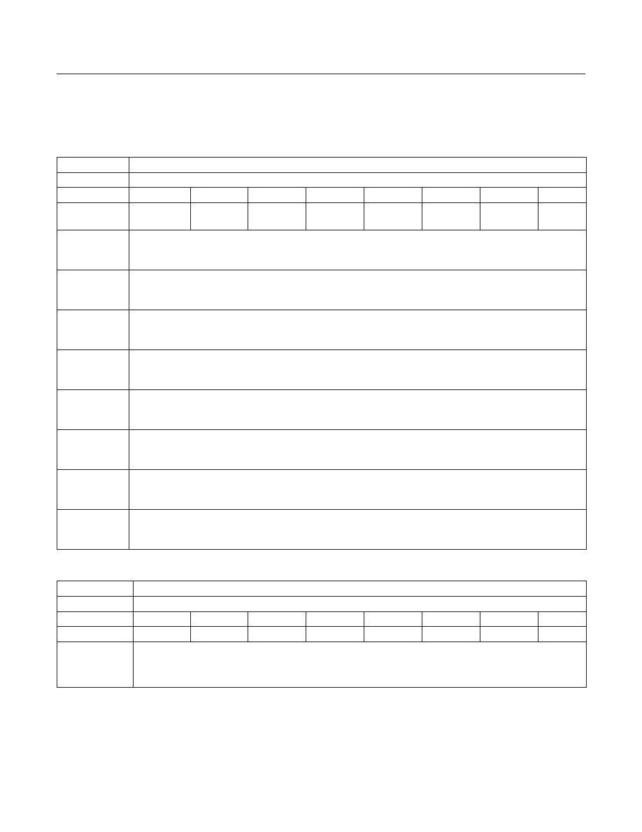
Table 22. DevInt1Mask Register (0x12)
Table 23. AICLIntMask Register (0x13)
ADDRESS:
0x12
MODE:
Read/Write
BIT
7
6
5
4
3
2
1
0
NAME
SysFltIM
ChgInOVPIM
ILimIM
VSysRegIM ThrmSd150IM ThrmSd120IM BatDetIM
WbChgIM
SysFltIM
SysFltI Interrupt Mask
1 = Mask
0 = Unmask
ChgInOVPIM
ChgInOVPI Interrupt Mask
1 = Mask
0 = Unmask
ILimIM
ILimI Interrupt Mask
1 = Mask
0 = Unmask
VSysRegIM
VSysRegI Interrupt Mask
1 = Mask
0 = Unmask
ThrmSd150IM
ThrmSd150I Interrupt Mask
1 = Mask
0 = Unmask
ThrmSd120IM
ThrmSd120I Interrupt Mask
1 = Mask
0 = Unmask
BatDetIM
BatDetI Interrupt Mask
1 = Mask
0 = Unmask
WbChgIM
WbChgI Interrupt Mask
1 = Mask
0 = Unmask
ADDRESS:
0x13
MODE:
Read/Write
BIT
7
6
5
4
3
2
1
0
NAME
-
AICLIM
-
-
-
-
-
-
AICLIM
AICLI Interrupt Mask
1 = Mask
0 = Unmask
MAX14748
USB Type-C Charger
www.maximintegrated.com
Maxim Integrated
46
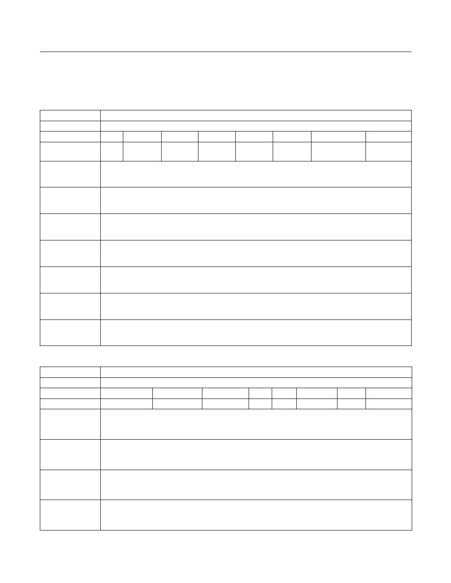
Table 24. DevInt2Mask Register (0x14)
Table 25. ChgIntMask Register (0x15)
ADDRESS:
0x14
MODE:
Read/Write
BIT
7
6
5
4
3
2
1
0
NAME
-
BattPREQIM BattUVLOIM BypUVLOIM SysUVLOIM DCDCILimIM DCDCRunAwayIM DCDCPGoodIM
BattPREQIM
BattPREQI Interrupt Mask
1 = Mask
0 = Unmask
BattUVLOIM
BattUVLOI Interrupt Mask
1 = Mask
0 = Unmask
BypUVLOIM
BypUVLOI Interrupt Mask
1 = Mask
0 = Unmask
SysUVLOIM
SysUVLOI Interrupt Mask
1 = Mask
0 = Unmask
DCDCILimIM
DCDCILimI Interrupt Mask
1 = Mask
0 = Unmask
DCDCRunAwayIM
DCDCRunAwayI Interrupt Mask
1 = Mask
0 = Unmask
DCDCPGoodIM
DCDCPGoodI Interrupt Mask
1 = Mask
0 = Unmask
ADDRESS:
0x15
MODE:
Read/Write
BIT
7
6
5
4
3
2
1
0
NAME
DirChgFaultIM
LowPowRIM
LowPowFIM
-
-
-
-
ChgStatIM
DirChgFaultIM
DirChgFaultI Interrupt Mask
1 = Mask
0 = Unmask
LowPowRIM
LowPowRI Interrupt Mask
1 = Mask
0 = Unmask
LowPowFIM
LowPowFI Interrupt Mask
1 = Mask
0 = Unmask
ChgStatIM
ChgStatI Interrupt Mask
1 = Mask
0 = Unmask
MAX14748
USB Type-C Charger
www.maximintegrated.com
Maxim Integrated
47
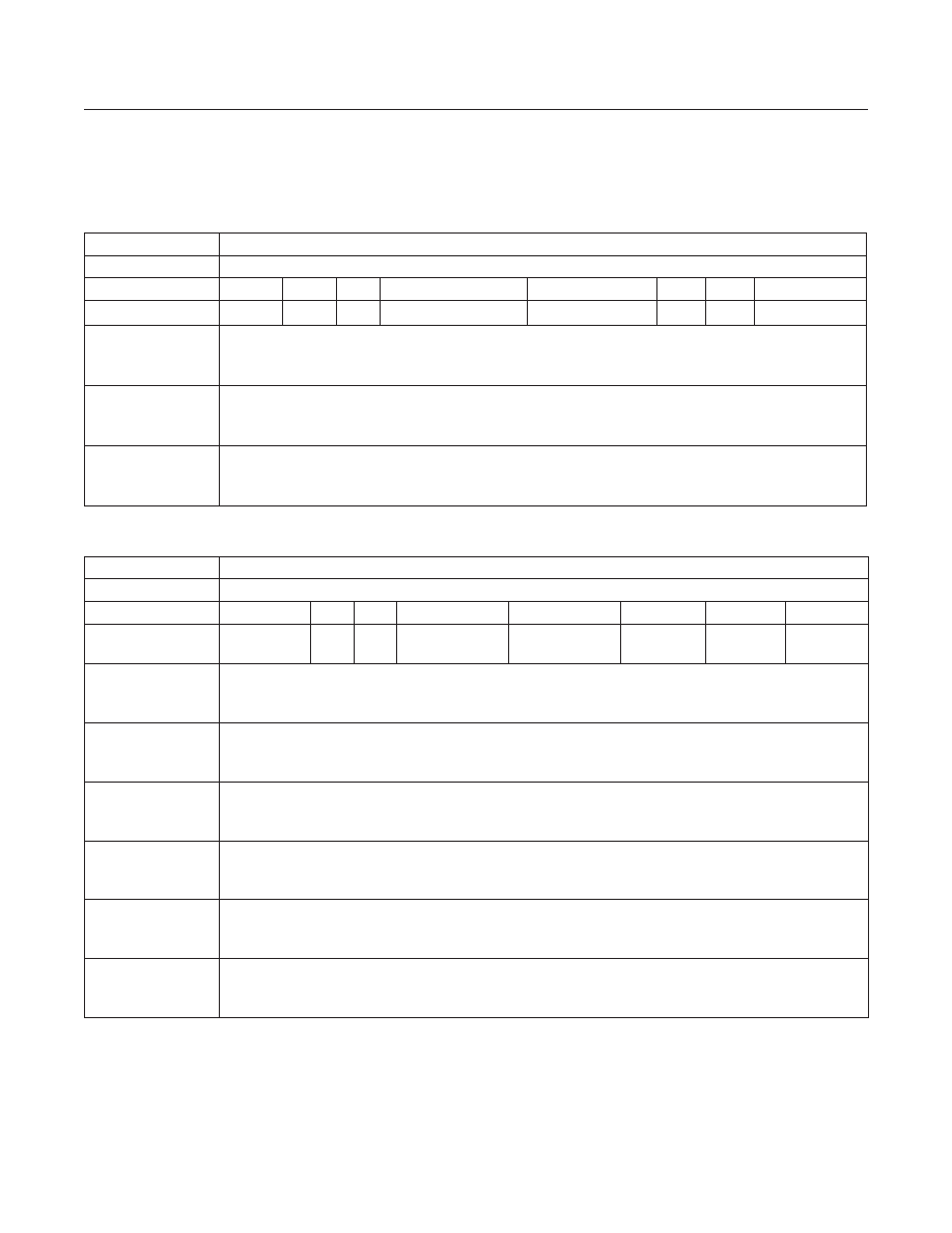
Table 26. JEITAIntMask Register (0x16)
Table 27. BCIntMask Register (0x17)
ADDRESS:
0x16
MODE:
Read/Write
BIT
7
6
5
4
3
2
1
0
NAME
-
-
-
ChgThrmRegCurIM
ChgThrmRegVltIM
-
-
ChgThrmStatIM
ChgThrmRegCurIM
ChgThrmRegCurI Interrupt Mask
1 = Mask
0 = Unmask
ChgThrmRegVltIM
ChgTHrmRegVI Interrupt Mask
1 = Mask
0 = Unmask
ChgThrmIM
ChgThrmI Interrupt Mask
1 = Mask
0 = Unmask
ADDRESS:
0x17
MODE:
Read/Write
BIT
7
6
5
4
3
2
1
0
NAME
VBUSDetIM
-
-
ChgTypRunFIM
ChgTypRunRIM PrChgTypIM DCDTmoIM ChgTypIM
VBUSDetIM
VBUSDetI Interrupt Mask
1 = Mask
0 = Unmask
ChgTypRunFIM
ChgTypRunFI Interrupt Mask
1 = Mask
0 = Unmask
ChgTypRunRIM
ChgTypRunRI Interrupt Mask
1 = Mask
0 = Unmask
PrChgTypIM
PrChgTypeI Interrupt Mask
1 = Mask
0 = Unmask
DCDTmoIM
DCDTmrI Interrupt Mask
1 = Mask
0 = Unmask
ChgTypIM
ChgTypI Interrupt Mask
1 = Mask
0 = Unmask
MAX14748
USB Type-C Charger
www.maximintegrated.com
Maxim Integrated
48
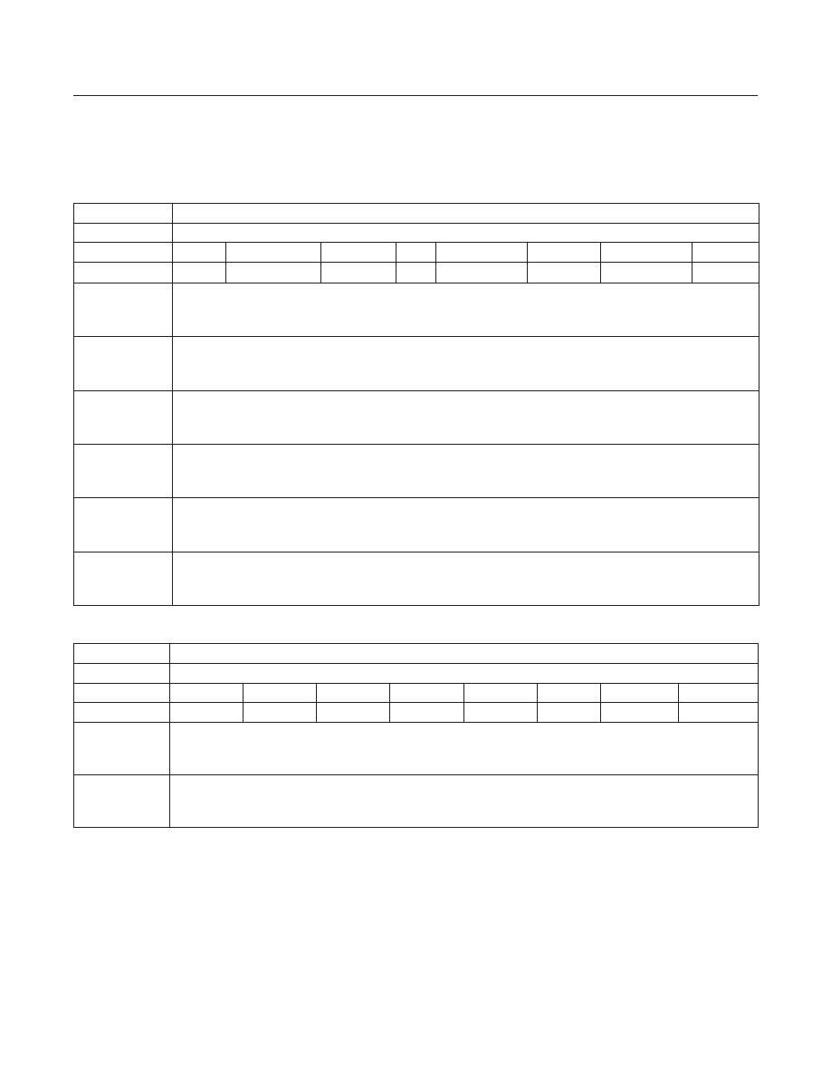
Table 28. CCIntMask Register (0x18)
Table 29. LED_CTRL Register (0x19)
ADDRESS:
0x18
MODE:
Read/Write
BIT
7
6
5
4
3
2
1
0
NAME
-
VSAFE0VIM
DetAbrtIM
-
CCPinStatIM
CCIStatIM
CCVcnStatIM
CCStatIM
VSAFE0VIM
VSAFE0VI Interrupt Mask
1 = Mask
0 = Unmask
DetAbrtIM
DetAbrtI Interrupt Mask
1 = Mask
0 = Unmask
CCPinStatIM
CCPinStatI Interrupt Mask
1 = Mask
0 = Unmask
CCIStatIM
CCIStatI Interrupt Mask
1 = Mask
0 = Unmask
CCVcnStatIM
CCVcnStatI Interrupt Mask
1 = Mask
0 = Unmask
CCStatIM
CCStatI Interrupt Mask
1 = Mask
0 = Unmask
ADDRESS:
0x19
MODE:
Read/Write
BIT
7
6
5
4
3
2
1
0
NAME
-
-
-
-
-
-
LEDCtrl
LEDManual
LEDCtrl
LED Manual Control
0 = LED is OFF
1 = LED is ON
LEDManual
LED Auto/Manual Configuration
0 = LED is controlled via charger state machine.
1 = LED output is manually controlled by LEDCntl bit.
MAX14748
USB Type-C Charger
www.maximintegrated.com
Maxim Integrated
49

Table 30. ThermaCfg1 Register (0x1A)
ADDRESS:
0x1A
MODE:
Read/Write
BIT
7
6
5
4
3
2
1
0
NAME
T1T2IFchg[2:0]
T2T3IFchg[2:0]
JeitaCfgR[1:0]
T1T2IFchg[2:0]
Fast Charge Current for T1-T2 temperature zone
000 = 0.2 x IFChg
001 = 0.3 x IFChg
010 = 0.4 x IFChg
011 = 0.5 x IFChg
100 = 0.6 x IFChg
101 = 0.7 x IFChg
110 = 0.8 x IFChg
111 = 1.0 x IFChg
T2T3IFchg[2:0]
Fast Charge Current for T2-T3 temperature zone
000 = 0.2 x IFChg
001 = 0.3 x IFChg
010 = 0.4 x IFChg
011 = 0.5 x IFChg
100 = 0.6 x IFChg
101 = 0.7 x IFChg
110 = 0.8 x IFChg
111 = 1.0 x IFChg
JeitaCfgR[1:0]
TPU SW Configuration
00 = JEITA Monitoring and TPU SW disabled
01 = JEITA Monitoring and TPU SW Enabled if V
CHGIN
> V
BDET
(10ms Debounce)
10 = JEITA Monitoring and TPU SW Enabled
11 = JEITA Monitoring disabled and TPU SW enabled
MAX14748
USB Type-C Charger
www.maximintegrated.com
Maxim Integrated
50
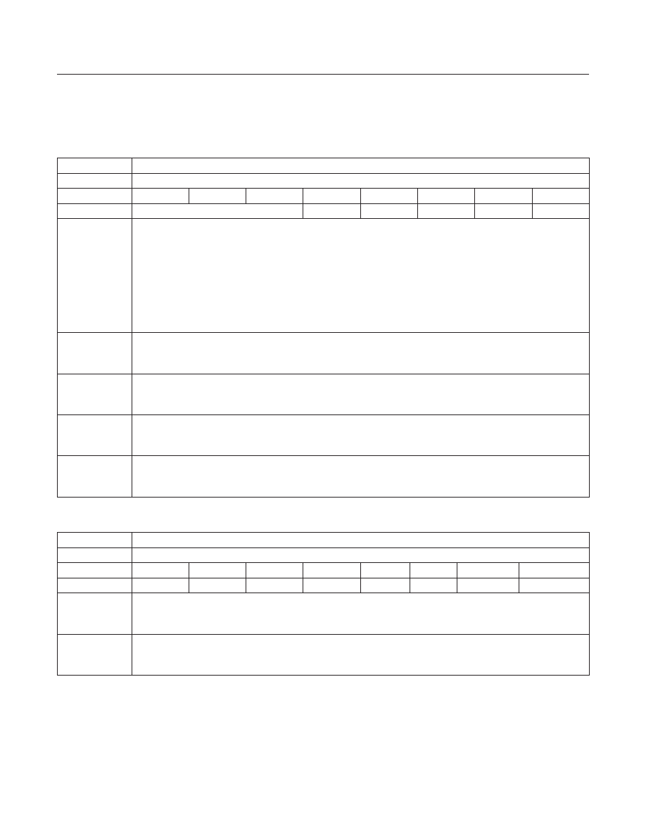
Table 31. ThermaCfg2 Register (0x1B)
Table 32. ThermaCfg3 Register (0x1C)
ADDRESS:
0x1B
MODE:
Read/Write
BIT
7
6
5
4
3
2
1
0
NAME
T3T4IFchg[2:0]
-
T3T4ENset T1T2ENset
T3T4VFset
T1T2VFset
T3T4IFchg[2:0]
Fast Charge Current for T3-T4 temperature zone
000 = 0.2 x IFChg
001 = 0.3 x IFChg
010 = 0.4 x IFChg
011 = 0.5 x IFChg
100 = 0.6 x IFChg
101 = 0.7 x IFChg
110 = 0.8 x IFChg
111 = 1.0 x IFChg
T3T4ENset
JEITA charger On/Off in T3-T4 zone. (Only valid if JEITACtrSet = 1)
0 = JEITA turns charger off in T3-T4 zone
1 = JEITA doesnt turn charger off in T3-T4 zone
T1T2ENset
JEITA charger On/Off in T1-T2 zone. (Only valid if JEITACtrSet = 1)
0 = JEITA turns charger off in T1-T2 zone
1 = JEITA doesnt turn charger off in T1-T2 zone
T3T4VFset
JEITA voltage scaling enable in T3-T4. (Only valid if JEITACtrSet = 1)
1 = Enabled
0 = Disabled
T1T2VFset
JEITA voltage scaling enabled in T1-T2. (Only valid if JEITACtrSet = 1)
1 = Enabled
0 = Disabled
ADDRESS:
0x1C
MODE:
Read/Write Unless Otherwise Noted
BIT
7
6
5
4
3
2
1
0
NAME
-
-
-
-
-
-
JEITACtrSet
WarmCoolSel
JEITACtrSet
JEITA Control Enable
0 = JEITA status Not affect charger
1 = JEITA status affects charger settings (See register ThermaCfg2)
WarmCoolSel
Warm/Cool JEITA Zone Thresholds Select (Read Only).
0 = 45 °C Warm, 10 °C Cool
1 = 25 °C Warm, 10 °C Cool
MAX14748
USB Type-C Charger
www.maximintegrated.com
Maxim Integrated
51

Table 33. ChargerCtrl1 Register (0x1D)
ADDRESS:
0x1D
MODE:
Read/Write or Ready-Only if AppWrtPrtct = (1) Protected (See Table 61)
BIT
7
6
5
4
3
2
1
0
NAME
ChgAutoStp
BatReChg[1:0]
-
-
BatReg[1:0]
ChgEn
ChgAutoStp
Charger Auto-Stop. Controls the transition from maintain charge to maintain charge done. See Battery Charger
State diagram.
0 = Auto-Stop disabled.
1 = Auto-Stop enabled.
BatReChg[1:0]
BAT Recharge Threshold. If ChgAutoSta = 1, charger restarts charging if V
BAT
falls below V
BATREG
by this
amount.
00 = 200mV
01 = 300mV
10 = 400mV
11 = 500mV
BatReg[1:0]
Battery Regulation Threshold
00 = 8.3V
01 = 8.4V
10 = 8.5V
11 = 8.6V
ChgEn
On/Off Control for Charger (does not impact SYS node).
0 = Charger disabled
1 = Charger enabled
MAX14748
USB Type-C Charger
www.maximintegrated.com
Maxim Integrated
52
Table 34. ChargerCtrl2 Register (0x1E)
Table 35. ChargerCtrl3 Register (0x1F)
ADDRESS:
0x1E
MODE:
Read/Write or Ready-Only if AppWrtPrtct = (1) Protected (See Table 61)
BIT
7
6
5
4
3
2
1
0
NAME
-
VPchg[2:0]
IPChg[1:0]
ChgDone[1:0]
VPchg[2:0]
Pre-charge Voltage Threshold Setting
000 = 5.7V
001 = 5.8V
010 = 5.9V
111 = 6.0V
100 = 6.1V
101 = 6.2V
110 = 6.3V
111 = 6.4V
IPChg[1:0]
Pre-charge Current Setting
00 = 0.05 x IFChg
01 = 0.1 x IFChg
10 = 0.2 x IFChg
11 = 0.3 x IFChg
ChgDone[1:0]
Charge Done Threshold Setting
00 = 0.05 x IFChg
01 = 0.1 x IFChg
10 = 0.2 x IFChg
11 = Reserved
ADDRESS:
0x1F
MODE:
Read/Write or Ready-Only if AppWrtPrtct = (1) Protected (See Table 61)
BIT
7
6
5
4
3
2
1
0
NAME
-
ChgAutoSta
MtChgTmr[1:0]
FChgTmr[1:0]
PChgTmr[1:0]
ChgAutoSta
Charger Auto-Restart Control
0 = Charger remains in maintain charge done even when V
BAT
is less than BAT recharge threshold.
1 = Charger automatically restarts when V
BAT
drops below BAT recharge threshold.
MtChgTmr[1:0]
Maintain Charge Timer Setting
00 = 0min
01 = 15min
10 = 30min
11 = 60min
FChgTmr[1:0]
Fast- Charge Timer Setting
00 = 75min
01 = 150min
10 = 300min
11 = 600min
PChgTmr[1:0]
Pre-charge Timer Setting
00 = 30min
01 = 60min
10 = 120min
11 = 240min
MAX14748
USB Type-C Charger
www.maximintegrated.com
Maxim Integrated
53
Table 36. ChargerCtrl4 Register (0x20)
Table 37. CurLimCtrl Register (0x21)
ADDRESS:
0x20
MODE:
Read-Only
Read/Write or Ready-Only if AppWrtPrtct =
(1) Protected (See Table 61)
BIT
7
6
5
4
3
2
1
0
NAME
WeakBatStat[2:0]
-
-
WeakBatEn
-
-
WeakBatStat[2:0]
Weak Battery FSM status
000 = Idle, charger is not SDP
001 = Battery condition check
010 = Weak Battery 2-minute counter running
011 = Good Battery.
100 = Weak Battery 2-minute counter expired
101-111 = Reserved
WeakBatEna
Weak Battery FSM Enable
0 = Disable
1 = Enable
ADDRESS:
0x21
MODE:
Read/Write
BIT
7
6
5
4
3
2
1
0
NAME
CurLim1Frc
FSUSMsk
-
CurLim1Set[4:0]
CurLim1Frc
Forced Input Current Limit Enable. When CurLim1Frc is 1, the input current limit is by the CurLim1Set[4:0].
0 = Not forced
1 = Forced
FSUSMsk
FSUS pin function mask. If FSUSMsk is 1, FSUS pin status is ignored.
0 = FSUS pin function enabled
1 = FSUS pin function disabled
CurLim1Set[4:0]
Forced Input Current Limit Value. The input current limit is forced to this value if CurLim1Frc is set to 1.
00000 = 0.10A
00001 = 0.20A
¦
11101 = 3.00A
11110 = Reserved
11111 = Reserved
MAX14748
USB Type-C Charger
www.maximintegrated.com
Maxim Integrated
54
Table 38. CurLimStatus Register (0x22)
Table 39. BBCFG1 Register (0x23)
ADDRESS:
0x22
MODE:
Read Only
BIT
7
6
5
4
3
2
1
0
NAME
CurLim2Rb[2:0]
SpvChgIlim[4:0]
CurLim2Rb[2:0]
Active Charger/Boost current as percent of the value set by R
SET
.
0 = 20%
1 = 30%
2 = 40%
3 = 50%
4 = 60%
5 = 70%
6 = 80%
7 = 100%
SpvChgIlim[4:0]
SpvChgIlim[4:0] shows the actual input current limit currently set.
00000 = 0.10A
00001 = 0.20A
¦
11101 = 3.00A
11110 = Reserved
11111 = Reserved
ADDRESS:
0x23
MODE:
Read/Write or Ready-Only if AppWrtPrtct = (1) Protected (See Table 61)
BIT
7
6
5
4
3
2
1
0
NAME
BoostRComp[3:0]
-
-
-
-
BoostRComp[3:0]
Sets the internal compensation resistor for the boost mode
0000 = 9.5kW
0001 = 17.3kW
0010 = 25.3kW
0011 = 33.2kW
0100 = 41.4kW
0101 = 49.2kW
0110 = 57.3kW
0111 = 65.1kW
1000 = 73.6kW
1001 = 81.4kW
1010 = 89.4kW
1011 = 97.2kW
1100 = 105.5kW
1101 = 113.3kW
1110 = 121.4kW
1111 = 129.2kW
MAX14748
USB Type-C Charger
www.maximintegrated.com
Maxim Integrated
55

Table 40. BBCFG2 Register (0x24)
ADDRESS:
0x24
MODE:
Read/Write or Ready-Only if AppWrtPrtct = (1) Protected (See Table 61)
BIT
7
6
5
4
3
2
1
0
NAME
-
-
-
BBFrcZX
BuckVSet[3:0]
BBFrcZX
BBFrcZX sets the Buck in forced ZX mode.
0 = Forced PWM Mode
1 = Forced ZX Mode
BuckVSet[3:0]
Buck Regulation Voltage
0000 = 4.0V
0001 = 4.1V
0010 = 4.2V
0011 = 4.3V
0100 = 4.4V
0101 = 4.5V
0110 = 4.6V
0111 = 4.7V
1000 = 4.8V
1001 = 4.9V
1010 = 5.0V
1011 = 5.1V
1100 = 5.2V
1101 = 5.3V
1110 = 5.4V
1111 = 5.5V
MAX14748
USB Type-C Charger
www.maximintegrated.com
Maxim Integrated
56

Table 41. BCCtrl1 Register (0x25)
ADDRESS:
0x25
MODE:
Read/Write
BIT
7
6
5
4
3
2
1
0
NAME
DCD2s
SfOutLvl
-
ADC3PDet
SfOutCtrl[1:0]
ChgDetMan
ChgDetEn
DCD2s
DCD2s sets the timing of DCD in BC1.2
0 = standard
1 = 2s
SfOutLvl
SFOUT Voltage Level Select
0 = 5V
1 = 3.3V
ADC3PDet
3A DCP Detection Enable (adds detection step after BC1.2 completes to detect presence of 3A DCP)
0 = Not Enabled
1 = Enabled
SfOutCtrl[1:0]
Safe Out LDO SFOUT Control
00 = Always Disabled
01 = On if a valid CHGIN voltage is present
10 =Turns on under following conditions.
a. ChgDetEn = 1, CHGIN is valid, and BC1.2 FSM Detection is finished
b. ChgDetEn = 0, and CHGIN is valid
11: RFU
Note: CHGIN valid can be external CHGIN voltage or CHGIN voltage generated by reverse buck in Attached.
SRC_CCx mode. A system that supports power swap must not use SFOUT LDO to supply USB transceiver.
According to USB PD specification, CHGIN will collapse during power swap. This turns off SFOUT LDO which is
supplied from CHGIN, and kills USB communication.
ChgDetMan
ChgDetMan forces manual run of charger detection. (Bit auto-resets to 0)
0 = Not enabled
1 = Request manual run of charger detection
ChgDetEn
Charger Detection Enable
0 = Not enabled
1 = Enabled (charger detection runs every time V
CHGIN
> V
BDET
and DetAbrt = 0)
MAX14748
USB Type-C Charger
www.maximintegrated.com
Maxim Integrated
57
Table 43. CCCtrl1 Register (0x27)
Table 42. Reserved Register (0x26)
ADDRESS:
0x27
MODE:
Read/Write
BIT
7
6
5
4
3
2
1
0
NAME
-
-
-
-
CCSnkSrc
CCDbgEn
CCAudEn
CCDetEn
CCSnkSrc
Allow State machine to enter Source Mode (DFP) detection. Note USB PD role swap is allowed to enter Source
mode.
0 = Disable
1 = Enabled
CCDbgEn
Enable Detection of Type-C Debug Adapter
0 = Disabled
1 = Enabled
CCAudEn
Enable Detection of Type-C Audio Adapter
0 = Disabled
1 = Enabled
CCDetEn
Enable CC Pin Detection - Force State Machine to Disabled State.
0 = Disabled
1 = Enabled
ADDRESS:
0x26
MODE:
Read Only
BIT
7
6
5
4
3
2
1
0
NAME
-
-
-
-
-
-
-
-
MAX14748
USB Type-C Charger
www.maximintegrated.com
Maxim Integrated
58

Table 44. CCCtrl2 Register (0x28)
ADDRESS:
0x28
MODE:
Read/Write
BIT
7
6
5
4
3
2
1
0
NAME
CCForceError SnkAttachedLock CCSnkSrcSwp CCSrcSnkSwp CCVcnSwp CCVcnEn CCSrcRst CCSnkRst
CCForceError
Bit resets to 0 after a write (This bit resets to 0 automatically when action is done)
0 = No action
1 = Force transition to ErrorRecovery state.
SnkAttachedLock
Bit resets to 0 after a minimum of 1.1s
0 = Exit Attached.SNK* state when V
CHGIN
< V
BDET
for more than t
PDDEB
1 = Locked in Attached.SNK* state for a minimum of 1.1s if VBUS not present
CCSnkSrcSwp
USB PD Power role swap from Source to Sink. This bit must be written to 0 once the USB PD controller
completes the power role swap sequence
0 = No Swap Requested
1 = Swap Requested
CCSrcSnkSwp
USB PD Power role swap from Sink to Source. This bit must be written to 0 once the USB PD controller
completes the power role swap sequence
0 = No Swap Requested
1 = Swap Requested
CCVcnSwp
Signal State Machine to Swap V
CONN
roles. Bit resets to 0 after a write (Note this bit will reset to 0
automatically when action is done)
0 = No change in V
CONN
role
1 = force change in V
CONN
CCVcnEn
Force state of V
CONN
0 = Force V
CONN
off (both external Buck converter and V
CONN
switch)
1 = Automatic operation based on State Machine
CCSrcRst
Force a reset of the State Machine - Immediate transition to Unattached.SRC* state. Bit resets to 0 after a write.
0 = No reset
1 = Request reset
CCSnkRst
Force a reset of the State Machine - Immediate transition to Unattached.SNK* state. Bit resets to 0 after a write.
0 = No reset
1 = Request reset
* Attached.SNK, Unattached.SRC, and Unattached.SNK are defined in USB Type-C Specificaiton Release 1.1.
MAX14748
USB Type-C Charger
www.maximintegrated.com
Maxim Integrated
59
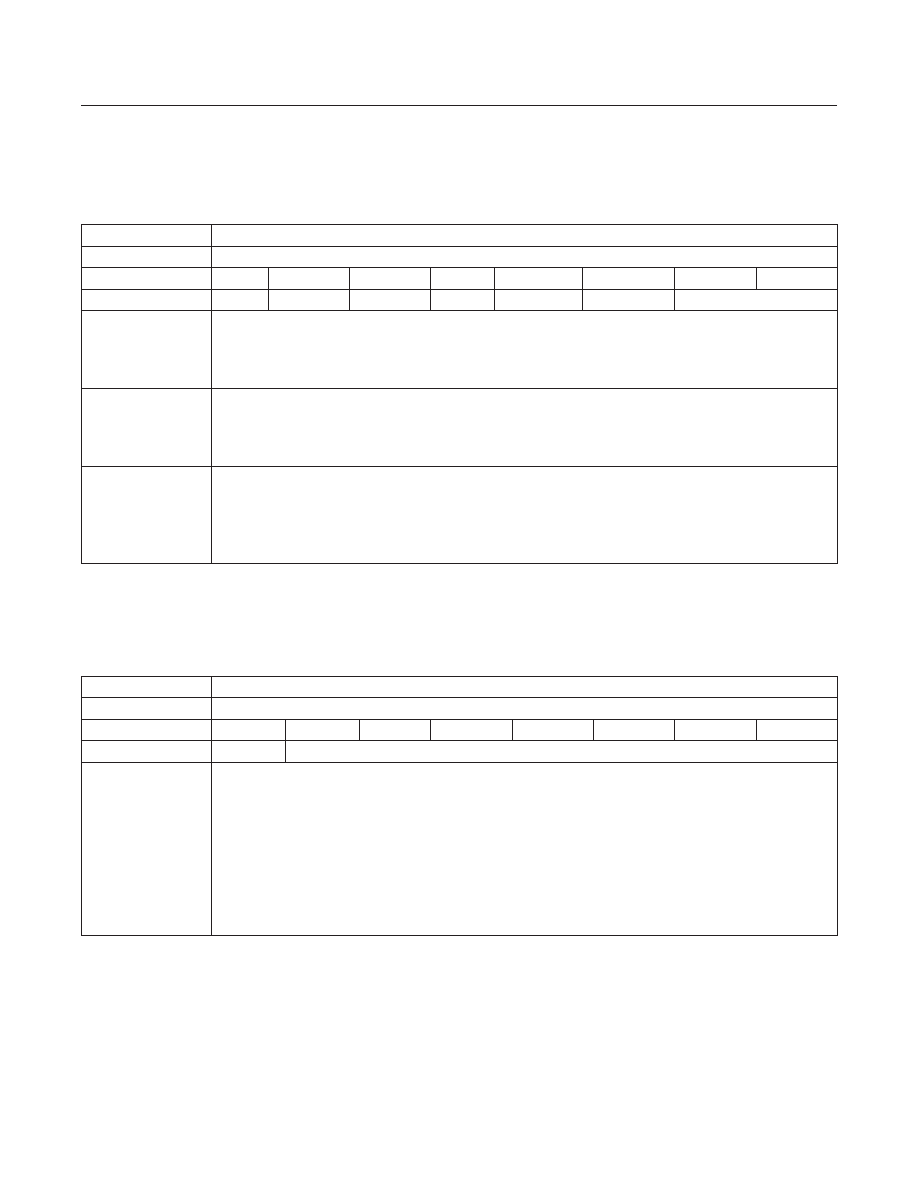
Table 45. CCCtrl3 Register (0x29)
Table 46. CHGINILim1 Register (0x2A)
ADDRESS:
0x29
MODE:
Read/Write
BIT
7
6
5
4
3
2
1
0
NAME
-
-
-
-
CCTrySnk
CCPreferSnk
CCDRPPhase[1:0]
CCTrySnk
Enable transition from AttachWait.SRC* to Try.SNK* then to Attach.SNK_CCx* or to TryWait.SRC* for DRP
that strongly prefers the SNK role. CCTrySnk has higher priority than CCPreferSnk.
0 = Disabled
1 = Enabled
CCPreferSnk
Enable transition from Unattached.SRC* to Try.SNK* then to Unattached.SNK* for DRP that strongly prefers
the SNK role.
0 = Disabled
1 = Enabled
CCDRPPhase[1:0]
Percent of time device is acting as Unattached.SRC* when CCSNKSRC = 1
00 = 35%
01 = 40%
10 = 45%
11 = 50%
ADDRESS:
0x2A
MODE:
Read Only
BIT
7
6
5
4
3
2
1
0
NAME
-
CHGINILim[6:0]
CHGINILim[6:0]
Status of charger input current limit set by charger detection (in 33mA step). Note that the first 4 codes are
all 100mA.
0000000 = 100mA
0000001 = 100mA
0000010 = 100mA
0000011 = 100mA
0000100 = 133mA
0000011 = 166mA
¦
1111111 = 4059mA
* AttachWait.SRC, Try.SNK, Attached.SNK, TryWait.SRC, Unattached.SNK, and Unattached SRC are defined in USB Type-C
Specificaiton Release 1.1.
MAX14748
USB Type-C Charger
www.maximintegrated.com
Maxim Integrated
60
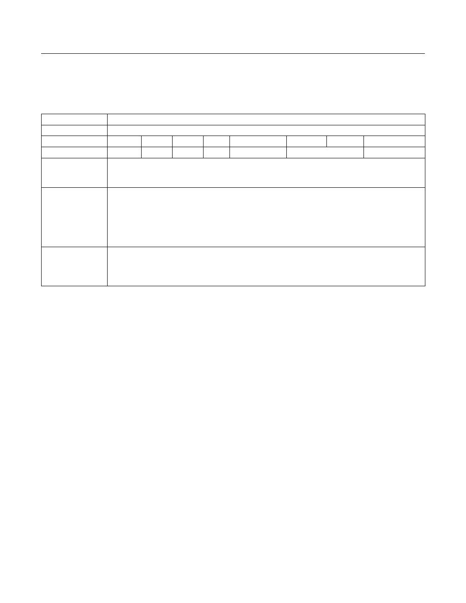
Table 47. CHGINILim2 Register (0x2B)
ADDRESS:
0x2B
MODE:
Read/Write
BIT
7
6
5
4
3
2
1
0
NAME
-
-
-
-
CHGINILimGate
SDPMaxCur[1:0]
CDPMaxCur
CHGINILimGate
CHGINILim Control options
0 = No gating of CHGINILim setting by BC1.2 FSM
1 = Gate changes in CHGINILim until BC1.2 FSM completes - ChgTypRun = 0
SDPMaxCur[1:0]
SDP Nonstandard Type-C Cable Control. USB-C to USB-A cables may have incorrect CC resistor
indicating 1.5A or 3A. Requires CHGINILimGate = 1.
00 = No modification of CHGIN_LIM
01 = Limit SDP to 500mA. ChgTyp = 01 (SDP) and PrChgTyp = 000 (unknown) set CHGINILim[6:0] to 0x0F
10 = Limit SDP to 1.0A. ChgTyp = 01 (SDP) and PrChgTyp = 000 (unknown) set CHGINILim[6:0] to 0x1E
11 = Limit SDP to 1.5A. ChgTyp = 01 (SDP) and PrChgTyp = 000 (unknown) set CHGINILim[6:0] to 0x2D
CDPMaxCur
CDP Nonstandard Type-C cable control. USB-C to USB-A cables may have incorrect CC resistor indicating
3A. Requires CHGIN_LIM_Gate = 1.
0 = No modification of CHGIN_LIM
1 = Limit CDP to 1.5A. ChgTyp = 10 (CDP) and PrChgTyp = 000 (unknown) set CHGINILim[6:0] to 0x2D
MAX14748
USB Type-C Charger
www.maximintegrated.com
Maxim Integrated
61
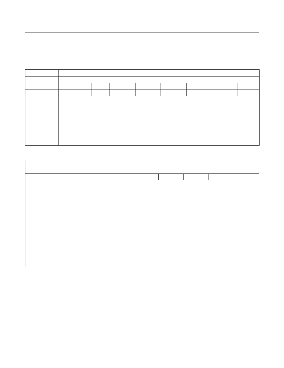
Table 48. AICLCFG1 Register (0x2C)
Table 49. AICLCFG2 Register (0x2D)
ADDRESS:
0x2C
MODE:
Read/Write or Ready-Only if AppWrtPrtct = (1) Protected (See Table 61)
BIT
7
6
5
4
3
2
1
0
NAME
AICLEn
-
-
-
-
-
-
AICLAbort
AICLEn
AICL Enable. Writing 1 to AICLEn enables AICL operation. Note that if AICLAbort is 1, AICL operation is not
allowed. This bit auto-resets to 0.
0 = No Action
1 = AICL enabled
AICLAbort
High Priority AICL Abort.
0 = Device is allowed to run AICL by writing 1 to AICLEn.
1 = Device is NOT allowed to run AICL operation. AICL operation will be aborted if its already running.
ADDRESS:
0x2D
MODE:
Read/Write or Ready-Only if AppWrtPrtct = (1) Protected (See Table 61)
BIT
7
6
5
4
3
2
1
0
NAME
BYPUVLO[2:0]
AICLMaxI[4:0]
BYPUVLO[2:0]
VBUS Theshold below which AICL stops incrementing the current
000 = 3.8V
001 = 3.9V
010 = 4.0V
011 = 4.1V
100 = 4.2V
101 = 4.3V
110 = 4.4V
111 = 4.5V
AICLMaxI[4:0]
AICL Stop Current (in 100mA step)
00000 = 100mA
00001 = 200mA
¦
11111 = 3.2A
MAX14748
USB Type-C Charger
www.maximintegrated.com
Maxim Integrated
62
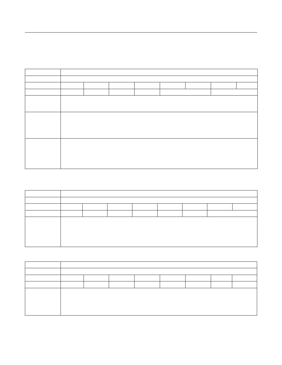
Table 50. AICLCFG3 Register (0x2E)
Table 51. DPDNSw Register (0x2F)
Table 52. Others Register (0x30)
ADDRESS:
0x2E
MODE:
Read/Write or Ready-Only if AppWrtPrtct = (1) Protected (See Table 61)
BIT
7
6
5
4
3
2
1
0
NAME
-
-
-
BYPDeb
AICLTBlk[1:0]
AICLTStep[1:0]
BYPDeb
AICL BYPUVLO[2:0] Rise Threshold Debounce Setting
0 = 500ms
1 = 200ms
AICLTBlk[1:0]
TBLANK Time Setting
00 = 500ms
01 = 1s
10 = 1.5s
11 = 5s
AICLTStep[1:0]
TSTEP Time Setting
00 = 100ms
01 = 200ms
10 = 300ms
11 = 500ms
ADDRESS:
0x2F
MODE:
Read/Write
BIT
7
6
5
4
3
2
1
0
NAME
-
-
-
-
-
-
AnSwCntl[1:0]
AnSwCntl[1:0]
AnSwCntl Analog Switch Configuration
00 = Auto. Switch is open during adapter detection. Switch closes if SDP or CDP is detected.
01 = Auto in SDP or CDP and Buck mode is detected.
10 = Switch forced open
11 = Switch forced closed
ADDRESS:
0x30
MODE:
Read/Write
BIT
7
6
5
4
3
2
1
0
NAME
-
-
-
-
-
-
-
USBCRSet
USBCRSet
USB-C Registers Reset. Writing 1 to USBCRSet resets registers associated with USB-C operation. (Note that
this operation opens the input limiter and turns off the boost converter temporarily.) Reset types are RST3 and
RST4. See Table 59 and Table 60 for more details. This bit auto-resets to 0.
0 = No Action
1 = Reset Registers
MAX14748
USB Type-C Charger
www.maximintegrated.com
Maxim Integrated
63
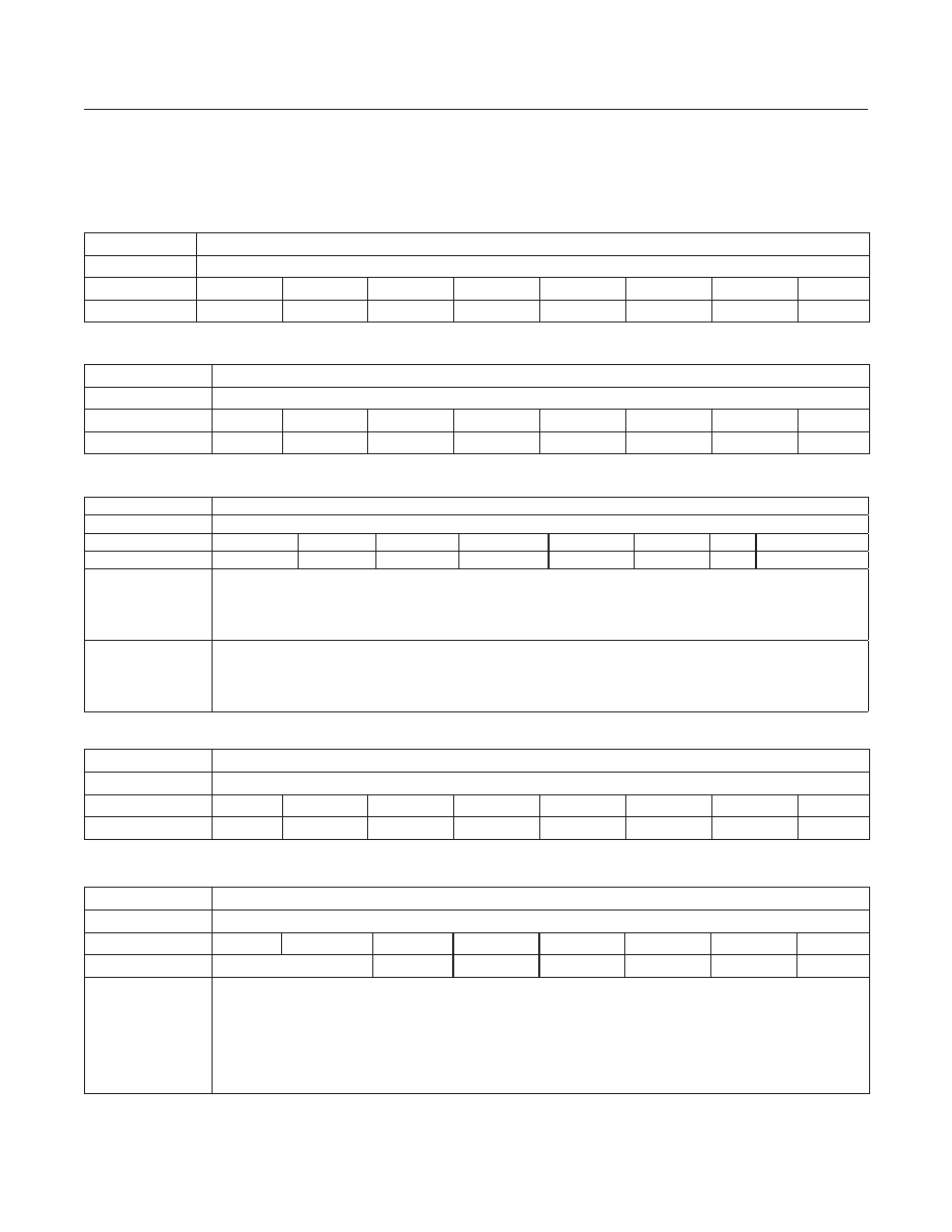
Table 53. Reserved Register (0x31)
Table 54. Reserved Register (0x32)
Table 55. LowPow Register (0x33)
Table 56. Reserved Register (0x34)
Table 57. FLTSel Register (0x35)
ADDRESS:
0x31
MODE:
Read Only
BIT
7
6
5
4
3
2
1
0
NAME
-
-
-
-
-
-
-
-
ADDRESS:
0x32
MODE:
Read Only
BIT
7
6
5
4
3
2
1
0
NAME
-
-
-
-
-
-
-
-
ADDRESS:
0x33
MODE:
Read/Write
BIT
7
6
5
4
3
2
1
0
NAME
LowPowEn
-
-
-
-
-
-
LowPowAbort
LowPowEn
Low Power Mode Enable. Set LowPowEn to 1 to enter Low Power mode. Note that if LowPowAbort is 1, Low
Power Mode is not allowed. This bit auto-resets to 0.
0 = No Action
1 = Enter Low Power mode
LowPowAbort
High Priority Low Power Mode Abort
0 = Device is allowed to enter Low Power mode by writing 1 to LowPowEn.
1 = Device is NOT allowed to enter Low Power Mode. Low Power Mode will be exited if device has already
entered it.
ADDRESS:
0x34
MODE:
Read Only
BIT
7
6
5
4
3
2
1
0
NAME
-
-
-
-
-
-
-
-
ADDRESS:
0x35
MODE:
Read/Write
BIT
7
6
5
4
3
2
1
0
NAME
FLTSelect[1:0]
-
-
-
-
-
-
FLTSelect[10]
FLTIN Charger-Faulting and External Reset Function Enable
00 = No effect and internally ignored
01 = Low on FLTIN pin (60ms debounce) places the charger in Battery Fault Charge Suspend state
(ChgStat[3:0] = 1000).
1x = Falling edge on FLTIN pin resets all registers. Reset types are RST1/RST2/RST3. See Table 59 and
Table 60 for more details.
MAX14748
USB Type-C Charger
www.maximintegrated.com
Maxim Integrated
64

RESET TYPE
RESET CONDITION
RST
1. V
CCINT
Power-On Reset
RST1
1. V
CCINT
Power-On Reset or
2. FLTIN falling edge (only if FLTSelect[1] = 1)
RST2
1. V
CCINT
Power-On Reset or
2. FLTIN falling edge (only if FLTSelect[1] = 1) or
3. VBUSDet rising edge
RST3
1. V
CCINT
Power-On Reset or
2. FLTIN falling edge (only if FLTSelect[1] = 1) or
3. USB-C reset through USBCRSet (0x30[0])
APPLICATION INDUCTANCE
( µH)
R
DC
(MΩ)
SATURATION
CURRENT (A)
CURRENT
RATING (A)
SUGGESTED PARTS
3A Type-C
Adapters
2.2μH
26
4.2
3.7
Taiyo Yuden NRS6028T2R2NMGJ
2.2μH
80
3.5
2.8
BOURNS SRP4012TA-2R2M
Table 59. Reset Types
Table 58. Suggested Inductors
MAX14748
USB Type-C Charger
www.maximintegrated.com
Maxim Integrated
65
Appilications Information
Component Selection
The correct selection of external components ensures
high efficiency, low output ripple, and fast transient
response.
Inductor Selection
The MAX14748 is designed to use a 1.5μH or 2.2μH
inductor. See
for suggested inductors and
manufacturers.
BAT Capacitor Selection
BAT capacitor is required to keep the BAT voltage ripple
small and to ensure regulation loop stability. The BAT
capacitor must have low impedance at the switching
frequency. Ceramic capacitors with X5R or X7R dielectric
are highly recommended due to their small size, low ESR,
and small temperature coefficients.
BAT requires careful bypassing. In the PCB layout, place
BAT capacitor as close as possible to BAT to minimize
parasitic inductance. If making connections to BAT capacitor
through vias, ensure that the vias are rated for the
expected input current to avoid excess inductance and
resistance between the capacitor and BAT.
The recommended nominal BAT capacitance is 22μF,
however, after initial tolerance, bias voltage, aging, and
temperature derating, the effective capacitance must be
greater than 10μF. To ensure regulation loop stability, the
effective BAT capacitance should be chosen within the
range of 10μF to 30μF.
SYS Capacitor Selection
SYS capacitor acts as the output capacitor for the boost
converter when charging, and the input capacitor for
the reverse buck converter when the device is acting as
power source in DRP mode. SYS capacitor is required to
keep the SYS voltage ripple small and to ensure regu-
lation loop stability. It must have low impedance at the
switching frequency. Ceramic capacitors with X5R or X7R
dielectric are highly recommended due to their small size,
low ESR, and small temperature coefficients.
Place SYS capacitor as close as possible to SYS to minimize
parasitic inductance. If making connections to SYS
capacitor through vias, ensure that the vias are rated for
the expected input current to avoid excess inductance
and resistance between the capacitor and SYS.
The recommended nominal SYS capacitance is 40μF,
however, after initial tolerance, bias voltage, aging, and
temperature derating, the effective capacitance must be
greater than 15μF.
BYP Capacitor Selection
BYP capacitor acts as the input capacitor for the boost
con ¬verter, and the output capacitor for the reverse buck
converter. BYP capacitor reduces the current peaks
drawn from the input power source when charging while
reducing the output voltage ripple of the reverse buck
converter when it is acting as power source in DRP mode.
The impedance of the input capacitor at the switching fre-
quency should be very low. Ceramic capacitors with X5R
or X7R dielectric are highly recommended due to their
small size, low ESR, and small temperature coefficients.

MAX14748
USB Type-C Charger
www.maximintegrated.com
Maxim Integrated
66
BYP requires careful bypassing. In the PCB layout, place
BYP capacitor as close as possible to the BYP to mini-
mize parasitic inductance. If making connections to BYP
capacitor through vias, ensure that the vias are rated for
the expected input current to avoid excess inductance
and resistance between the capacitor and BYP.
The recommended nominal BYP capacitance is 22μF,
however, after initial tolerance, bias voltage, aging, and
temperature derating, the effective capacitance must be
greater than 10μF.
CHGIN Capacitor Selection
CHGIN capacitor decouples a charge source and its
parasitic impedance. Typically, the charger source at
CHGIN is a USB connectors VBUS. The recommended
nominal CHGIN capacitance is 1μF. Larger capacitance
at CHGIN improves the decoupling; how ¬ever, take care
not to exceed the maximum capacitance allowed by the
USB specification.
The impedance of the CHGIN at the DC-DC switching fre-
quency should be very low. Ceramic capacitors with X5R
or X7R dielectric are highly recommended due to their
small size, low ESR, and small temperature coefficients.
To fully utilize the +30V input capability of the, choose a
capacitor with a 35V or greater rating; many appli ¬cations
dont need to utilize the full input capability of the device
and find that a 16V or 10V rated input capacitor is suf-
ficient.
BST Capacitor Selection
Choose the nominal BST capacitance to be 0.1μF. BST
capacitor is part of a charge pump that creates the high-
side gate drive for the DC-DC. It is recommended that the
BST capacitor has at least 10V rating.
PCB Layout and Routing
High switching frequencies and large peak currents
make PCB layout a very important part of design. Good
design minimizes excessive EMI on the feedback paths
and voltage gradients in the ground plane, both of which
can result in instability or regulation errors. Connect the
inductor, input capacitors, and output capacitors as close
together as possible, and keep their traces short, direct,
and wide. Keep noisy traces, such as the LX node, as
short as possible.
MAX14748
USB Type-C Charger
www.maximintegrated.com
Maxim Integrated
67
Table 60. Register Reset Types and Default Values
REGISTER
ADDRESS
REGISTER
NAME
RESET
TYPE
MAX14748
0x00
ChipID
RST1
0x3E
0x01
ChipRev
RST1
0x33
0x02
DevStatus1
RST1
STATUS*
0x03
AICLStatus
RST1
STATUS
0x04
DevStatus2
RST1
STATUS
0x05
ChgStatus
RST1
STATUS
0x06
JEITAStatus
RST1
STATUS
0x07
BCStatus
RST3
STATUS
0x08
Reserved
-
0x00
0x09
CCStatus1
RST3
STATUS
0x0A
CCStatus2
RST3
STATUS
0x0B
DevInt1
RST1
INT*
0x0C
AICLInt
RST1
INT
0x0D
DevInt2
RST1
INT
0x0E
ChgInt
RST1
INT
0x0F
JEITAInt
RST1
INT
0x10
BCInt
RST3
INT
0x11
CCInt
RST3
INT
0x12
DevInt1Mask
RST1
0xFF
0x13
AICLIntMask
RST1
0x40
0x14
DevInt2Mask
RST1
0x7F
0x15
ChgIntMask
RST1
0xF1
0x16
JEITAIntMask
RST1
0x19
0x17
BCIntMask
RST3
0xFF
0x18
CCIntMask
RST3
0x7F
0x19
LED_CTRL
RST1
0x00
0x1A
ThermaCfg1
RST2
0x7D
0x1B
ThermaCfg2
RST2
0xEF
0x1C
ThermaCfg3
RST2
0x02
REGISTER
ADDRESS
REGISTER
NAME
RESET
TYPE
MAX14748
0x1D
ChargerCtrl1
RST2
0x80
0x1E
ChargerCtrl2
RST2
0x10
0x1F
ChargerCtrl3
RST2
0x49
0x20
ChargerCtrl4**
RST2
0x06
0x21
CurLimCtrl
RST2
0x00
0x22
CurLimStatus
RST1
STATUS
0x23
BBCFG1
RST1
0x20
0x24
BBCFG2
RST1
0x8A
0x25
BCCtrl1
RST3
0x05
0x26
Reserved
-
0x00
0x27
CCCtrl1
RST3
0x19
0x28
CCCtrl2
RST3
0x04
0x29
CCCtrl3
RST3
0x08
0x2A
CHGINILim1
RST3
STATUS
0x2B
CHGINILim2
RST3
0x0B
0x2C
AICLCFG1
RST1
0x01
0x2D
AICLCFG2
RST1
0x44
0x2E
AICLCFG3
RST1
0x05
0x2F
DPDNSw
RST2
0x01
0x30
Others
RST1
0x00
0x31
Reserved
-
0x00
0x32
Reserved
-
0x00
0x33
LowPow
RST1
0x01
0x34
Reserved
-
0x01
0x35
FLTSel
RST
0x80
*INT and STATUS: status and interrupt register values vary
based on device operating condition.
** ChargerCtrl4 register value depends on the status of
WeakBatStat[2:0] bits.
MAX14748
USB Type-C Charger
www.maximintegrated.com
Maxim Integrated
68
Table 61. Register Bit Default Values
REGISTER BITS
VALUES
CDPMaxCur
1500mA
SDPMaxCur[1:0]
500mA
CHGINILimGate
Gating
CCAudEn
Disabled
CCDbgEn
Disabled
CCSnkSrc
Enabled
JeitaCfgR[1:0]
01
CCDRPPhase[1]
35% or 40%
CCTrySnk
Enabled
SfOutCtrl[1:0]
01
ADC3PDet
Disabled
DCD2s
Standard
WarmCoolSel
45 °C/10 °C
T1T2IFchg[2:0]
0.5 x IFChg
T3T4IFchg[2:0]
1.0 x IFChg
BatReg[1:0]
8.3V
ChgEn
Disabled
JETIACtrSet
(1) Control
IPChg[1:0]
0.05 x IFChg
ChgDone[1:0]
0.05 x IFChg
ChgAutoStp
Enabled
BatReChg[1:0]
100mV
FreshBatDis
Done
ChgAutoSta
Enabled
MtChTmr[1:0]
0min
FChgTmr[1:0]
300min
PChgTmr[1:0]
60min
ChipRevH[3:0]
3
AppWrtPrtct
(0) Writable
VPchg[2:0]
5.8V
T3T4ENset
Enabled
T1T2ENset
Enabled
T3T4VFset
Enabled
T1T2VFset
Enabled
T2T3IFchg[2:0]
1.0 x IFChg
BoostRComp[3:0]
2
REGISTER BITS
VALUES
FLTSelect[1:0]
(10) Reset
BuckVSet[3:0]
5.0V
AnSwCntl[1:0]
(01) Auto
AICLTStep[1:0]
200ms
WeakBatEna
Enabled
BYPUVLO{2:0]
4.0V
AICLMax[4:0]
500mA
BYPDeb
500 µs
AICLTBlk[1:0]
1000ms
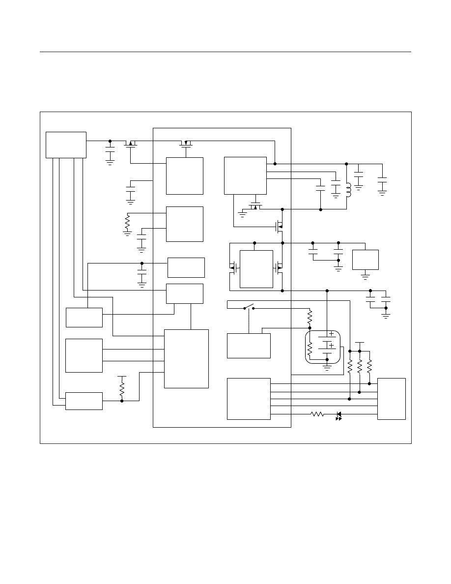
MAX14748
USB Type-C Charger
www.maximintegrated.com
Maxim Integrated
69
Typical Application Circuit
15W TYPE-C
ADAPTER
OVP and
CURRENT
LIMIT
CONTROL
REFERENCE
BIAS CIRCUITS
LINEAR
CHARGER
and
POWERPATH
CONTROL
PROTECTED
LDO
SYSTEM
USB
TX/RX
VCONN
SUPPLY
USB CHARGER
DETECTION
INTERFACE
USB SWITCH
BOOST-BUCK
CONTROLLER
SYSTEM
LOAD
I2C INTERFACE
AND CONTROL
LOGIC
JEITA
MANAGEMENT
SYSTEM
MICRO
SUPERSPEED
MUX
CHGIN
NVP
SET
V
CCINT
SFOUT
CDN, CDP
TDN, TDP
CC1, CC2
V
CONN
BVCEN
CDIR
VIO
VIO
THM
TPU
VTPU
BAT
FLTIN
SDA, SCL
INT
SYSOK
FSUS
LED
BYP
BREG
BST
LX
SYS
1 µF
0.1 µF
10 µF
L1
1 µF
0.1 µF
22 µF
10 µF
1 µF
1 µF
VBUS
COMP
3.9nF
0.1 µF
0.1 µF
Note: All capacitance values listed in this document refer to effective capacitance. Be sure to specify capacitors that will meet these
requirements under typical system operating conditions taking into consideration the effects of voltage and temperature.
+Denotes a lead(Pb)-free package/RoHS-compliant package.
See
for the device differences.
T = Tape and reel.
PART
TEMP RANGE
PIN-PACKAGE
MAX14748EWW+
-40 ºC to +85 ºC
54 WLP
MAX14748EWW+T
-40 ºC to +85 ºC
54 WLP
PACKAGE
TYPE
PACKAGE
CODE
OUTLINE
NO.
LAND
PATTERN NO.
54 WLP
W542C3+1
Refer to
MAX14748
USB Type-C Charger
www.maximintegrated.com
Maxim Integrated
70
Ordering Information
Chip Information
PROCESS: BiCMOS
Package Information
For the latest package outline information and land patterns
(footprints), go to
. Note
that a +, #, or - in the package code indicates RoHS status
only. Package drawings may show a different suffix character, but
the drawing pertains to the package regardless of RoHS status.

REVISION
NUMBER
REVISION
DATE
DESCRIPTION
PAGES
CHANGED
0
6/17
Initial release
Maxim Integrated cannot assume responsibility for use of any circuitry other than circuitry entirely embodied in a Maxim Integrated product. No circuit patent licenses
are implied. Maxim Integrated reserves the right to change the circuitry and specifications without notice at any time. The parametric values (min and max limits)
shown in the Electrical Characteristics table are guaranteed. Other parametric values quoted in this data sheet are provided for guidance.
Maxim Integrated and the Maxim Integrated logo are trademarks of Maxim Integrated Products, Inc.
MAX14748
USB Type-C Charger
© 2017 Maxim Integrated Products, Inc. 71
Revision History
For pricing, delivery, and ordering information, please contact Maxim Direct at 1-888-629-4642, or visit Maxim Integrateds website at www.maximintegrated.com.
Document Outline