| Secciones |
|---|
| Foros Electrónica |
|
|
| Boletines de correo |
 |
MOS IC
Semiconductor Group
60
01.96
Nonvolatile Memory 4-Kbit E
2
PROM
with
I
2
C Bus and Write Protection
SDA 3546-5
P-DIP-8-4
Circuit Description
I
2
C Bus Interface
The
I
2
C Bus is a bidirectional 2-line bus for the transfer of data between various integrated circuits.
It consists of a serial data line SDA and a serial clock line SCL. The data line requires an external
pull-up resistor to
V
CC
(open drain output stage).
The possible operational states of the
I
2
C Bus are shown in figure 1. In the quiescent state, both
lines SDA and SCL are high, i.e. the output stage of the data line is disabled. As long a SCL remain
"1", information changes on the data bus indicate the start or the end of data transfer between two
components.
The transition on SDA from "1" to "0" is a start condition, the transition from "0" to "1" is a stop
condition. During a data transfer the information on the data bus will only change while the clock line
SCL is "0". The information on SDA is valid as long as SCL is "1".
In conjunction with an
I
2
C Bus system, the memory component can operate as a receiver and as a
transmitter (slave receiver or slave transmitter). Between a start and stop condition, information is
always transmitted in byte-organized form. Between the falling edge of the eighth clock pulse and
a ninth acknowledge clock pulse, the memory component sets the SDA-line to low as a confirmation
of reception, if the chip select conditions have been met. During the output of data, the data output
of the memory is high in impedance during the ninth clock pulse (acknowledge master).
The necessary temporary signal function for the operation of the
I
2
C Bus is shown in figure 2.
Type
Ordering Code
Package
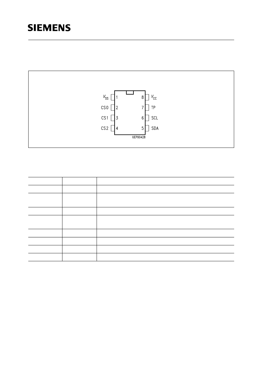
Pin Configuration
SDA 3546-5
Q67100-H5098
P-DIP-8-4
SIEMENS
Features
Word-organized programmable nonvolatile memory in
n-channel floating-gate technology (E
2
PROM)
512
×
8-bit organization
Supply voltage 5 V
Serial 2-line bus for data input and output (
I
2
C Bus)
Reprogramming mode, 10 ms erase / write cycle
Reprogramming by means of on-chip control (without
external control)
Check for end of programming process
Programming protect mode
Data retention > 10 years
More than 10
5
reprogramming cycles per address

SDA 3546-5
Semiconductor Group
61
Control Functions of the
I
2
C Bus
The memory component is controlled by the controller (master) via the
I
2
C Bus in two operating
modes: read-out cycle, and reprogramming cycle, including erase and write to a memory address.
In both operating modes, the controller, as transmitter, has to provide 3 bytes and an additional
acknowledge clock pulse to the bus after the start condition. During a memory read, at least nine
additional clock pulses are required to accept the data from the memory and the acknowledge
master, before the stop condition may follow. In the case of programming, the active programming
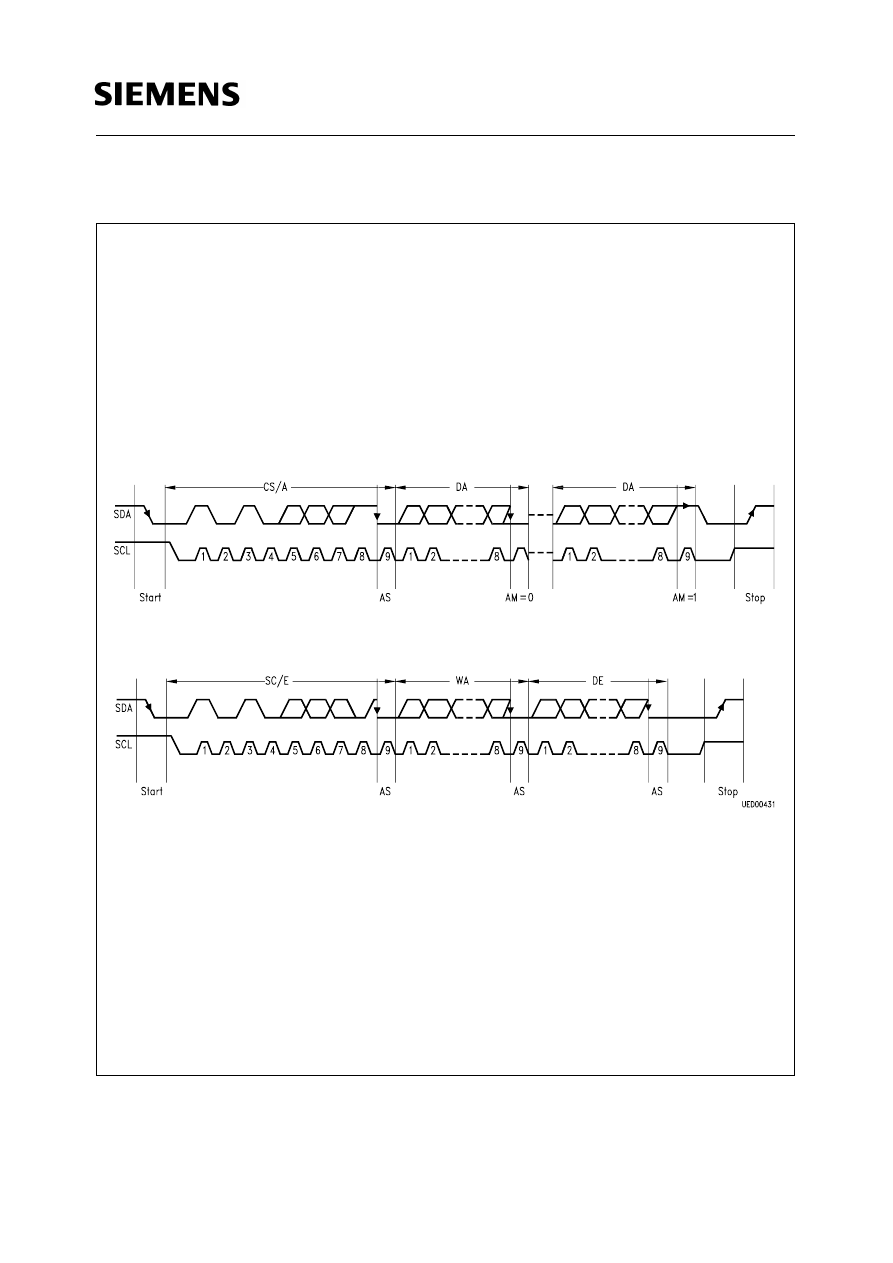
process is only started by the stop condition after data input (see figure 3).
The chip select word contains the chip select bit CS, thus allows 2 memory chips to be connected
in parallel. Chip select is achieved when the control bits logically correspond to the selected
conditions at the select inputs.
By means of the bit "Chip Select" CS/E the two bits A8 and A9 (MSB of the chip address) are
programmed.
Check for End of Programming or Abortion of Programming Process
If the chip is addressed during active reprogramming by entering CS/E, the programming process
is terminated. If, however, it is addressed by entering CS/A, the entry will be ignored. Only after
programming has been terminated will the chip respond to CS/A. This allows the user to check
whether the end of the programming process has been reached (see figure 3).
Memory Read
After the input of the first two control words CS/E and WA, a resetting of the start condition and the
input of the third control word CS/A, the memory is set ready to read. During acknowledge clock
nine, the memory information is transferred in parallel mode to the shift register. Subsequent to the
falling edge of the acknowledge clock, the data output is low impedance and the first data bit can be
sampled (see figure 4).
With every shift clock, an additional bit reaches the output. After reading a byte, the internal address
counter is automatically incremented when the master receiver switches the data line to "low"
during the ninth clock (acknowledge master). Any number of memory locations can thus be read
one after the other. At address 512, an overflow to address 0 is initiated. With the stop condition, the
data output returns to high-impedance mode. The internal sequence control of the memory
component is reset from the read to the quiescent state with the stop condition.

SDA 3546-5
Semiconductor Group
62
Memory Reprogramming
The reprogramming cycle of a memory word comprises an erase and a subsequent write process.
During erase, all eight bits of the selected word are set into the "1" state. During write, "0" states are
generated according to the information in the internal data register, i.e. according to the third input
control word. After the 27th and last clock of the control word input, the active programming process
is started by the stop condition. The active reprogramming process is executed under on-chip
control.
The time required for reprogramming depends on component deviation and data patterns.
Therefore, with rated supply voltage, the erase/write process extends over max. 20 ms, or more
typically, 10 ms. In the case of data word input without write request (write request is defined as data
bit in data register set to "0"), the write process is suppressed and the programming time is
shortened. During a subsequent programming of an already erased memory address, the erase
process is suppressed again, so that the reprogramming time is also shortened.
Important: Switch-On Mode and Chip Reset
After the supply voltage
V
CC
has been connected, the data output will be in high-impedance mode.
As a rule, the first operating mode to be entered, should be the read process of a word address.
As a result of the built-in "power-on reset" circuit, programming requests will not be accepted
immediately after the supply voltage has been switched on.
Total Erase
Enter the control word CS/E, load the address register with address 0 and the data register with FF
(hex) to erase the entire contents of the memory. Switch input CS2 to "open" immediately prior to
generating the stop condition. The subsequent stop condition triggers a total erase. Upon
termination of "total erase", CS2 must be reconnected to 0 V.
Write Protection Mode
When pin 2 is not connected, i. e. when CS0 is floating, this means that:
1) memory reprogramming is disabled.
2) the chip can only be addressed with chip select bit CS0 = 0 of control word CS/E or CS/A.
SDA 3546-5
Semiconductor Group
63
Pin Configuration
(top view)
Pin Definitions and Functions
Pin No.
Symbol
Function
1
V
SS
Ground
2
CS
Chip select 0
≤
V
I
≤
0.2 V; 4.5
≤
V
I
≤
V
CC
,
open, programming disabled condition
3
TP1
to
V
SS
4
TP2
0 V norm. operation, TP2 = 5 V
total erase condition
5
SDA
Data line
6
SCL
Clock line
7
TP3
Open
8
V
CC
Supply voltage
P-DIP-8-4
SDA 3546-5
Semiconductor Group
64
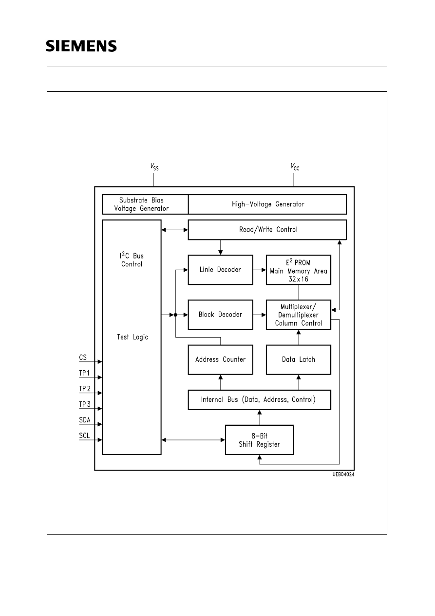
Block Diagram
SDA 3546-5
Semiconductor Group
65
Absolute Maximum Ratings
Parameter
Symbol
Limit Values
Unit
min.
max.
Supply voltage range
V
CC
- 0.3
6
V
Input voltage range
V
I
- 0.3
6
V
Power dissipation
P
D
130
mW
Storage temperature
T
stg
- 40
125
°C
Thermal resistance
(system-air)
R
th SA
100
K/W
Junction temperature
T
j
85
°C
Operating Range
Supply voltage
V
CC
4.75
5.25
V
Ambient temperature
T
A
0
70
°C
SDA 3546-5
Semiconductor Group
66
Characteristics
T
A
= 25 °C
Parameter
Symbol
Limit Values
Unit
Test Condition
min.
typ.
max.
Supply voltage
V
CC
4.75
5.0
5.25
V
Supply current
I
CC
20
mA
V
CC
= 5.25 V
Inputs
Input voltages SDA/SCL
V
IL
1.5
V
Input voltages SDA/SCL
V
IH
3.0
V
CC
V
Input currents SDA/SCL
I
IH
10
µ
A
V
IH
=
V
CC
Outputs
Output current
SDA
I
QL
3.0
mA
V
QL
= 0.4 V
Leakage current SDA
I
QH
10
µ
A
V
QH
=
V
CC max
Inputs
Input voltages CS/TP1/TP2
V
IL
0.2
V
Input voltages CS/TP1/TP2
V
IH
4.5
V
CC
V
Input currents CS/TP1/TP2
I
IH
100
µ
A
V
CC
= 5.25 V
Clock frequency
f
SCL
100
kHz
Reprogramming duration
t
PROG
10
20
ms
erase and write
Input capacity
C
I
10
pF
Total erase
t
GL
20
ms
TP2 = 5 V
SDA 3546-5
Semiconductor Group
67
Diagrams
Figure 1
Operation States of the
I
2
C Bus
SDA 3546-5
Semiconductor Group
68
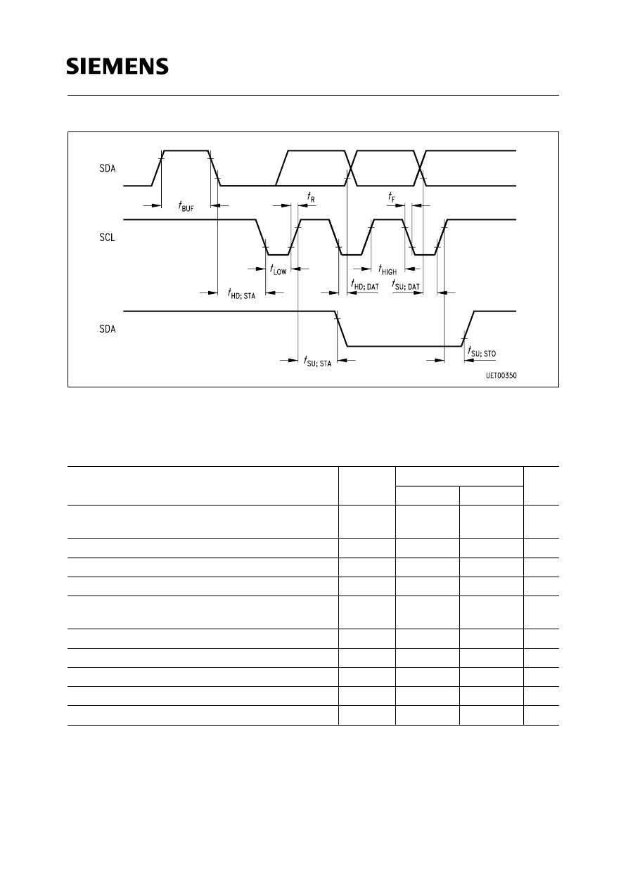
Figure 2
Timing Conditions for the
I
2
C Bus
Absolute Maximum Ratings
*) Note that a transmitter must internally provide at least a hold time to bridge the undefined region (max. 300 ns)
of the falling edge of SCL.
Parameter
Symbol
Limit Values
Unit
min.
max.
Minimum time the bus must be free
before a new transmission can start
t
BUF
4.7
µ
s
Start condition hold time
t
HD;STA
4.0
µ
s
Clock low period
t
LOW
4.7
µ
s
Clock high period
t
HIGH
4.0
µ
s
Start condition set-up time,
only valid for repeated start code
t
SU;STA
4.7
µ
s
Data set-up time
t
SU;DAT
250
ns
Rise time of both the SDA and SCL line
t
R
1
µ
s
Fall time of both the SDA and SCL line
t
F
300
ns
Stop condition set-up time
t
SU;STO
4.7
µ
s
Hold time data
t
HD;DAT
0*)
SDA 3546-5
Semiconductor Group
69
Figure 3
Programming
Control word input
Figure 4
Read
Control word input read
a) complete (with word address input)
ST
CS/E
As
WA
As
DE
As
SP
(the reprogramming starts after
this stop condition)
ST
CS/A
As
Check for program end by
1. when As = 1 programming is not finished
2. when As = 0 programming is finished
Program interruption by
ST
CS/E
As
ST
CS/E
As
WA
As
ST
CS/A
As
DA
Am
DA
Am
SP
n bytes
Last byte
Automatic incrementation
of the word address
ST
CS/A
As
DA
Am
DA
Am
SP
b) shortened:
Bit 0 ¦ 8 the last selected word
address remain unchanged
n bytes
Last byte
Autoincrement
Am = 0
before stop condition
Am = 1
SDA 3546-5
Semiconductor Group
70
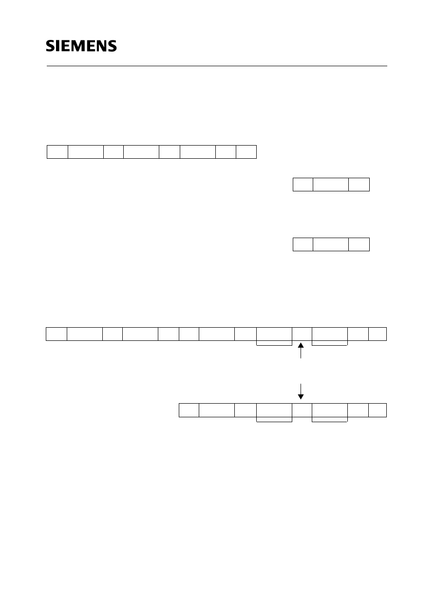
Control Word Table
Control Word Input Key
Clock No.
1
2
3
4
5
6
7
8
9
(Acknowledge)
CS/E
CS/A
WA
DE
DA
1
0
1
0
CS2 CS1 CS
0
0
1
0
1
0
CS2 CS1 CS
1
0
A7
A6
A5
A4
A3
A2
A1
A0
0
D7
D6
D5
D4
D3
D2
D1
D0
0
D7
D6
D5
D4
D3
D2
D1
D0
0/1
through memory
through memory
through memory
through memory
through master
CS/E
Chip select for data input into memory
CS/A
Chip select for data output out of memory
WA
Memory word address
DE
Data word for memory
DA
Data word read out of memory
D0 to D7
Data bits
ST
Start condition
SP
Stop condition
As
Acknowledge bit from memory
Am
Acknowledge bit from master
CS0, CS1, CS2
Chip select bit
A0 to A8
Memory word address bits

